
 Open Access Article
 This Open Access Article is licensed under a
 Creative Commons Attribution 3.0 Unported Licence
Two-step vapor transport deposition of large-size bridge-like Bi2Se3 nanostructures
Manshu
Han
,
Jiangang
Ma
*,
Haiyang
Xu
* and
Yichun
Liu
Centre for Advanced Optoelectronic Functional Materials Research and Key Laboratory for UV Light-Emitting Materials and Technology of Ministry of Education, Northeast Normal University, Changchun 130024, China. E-mail: majg@nenu.edu.cn; hyxu@nenu.edu.cn; Fax: +86 431 85099772; Tel: +86 431 85099767
First published on 25th September 2015
Abstract
In this paper, single crystalline Bi2Se3 nanostructures including nanowires, nanoribbons, nanoplates and bridge-like nanostructures have been grown by physical vapor deposition. By investigating the morphological evolution of the Bi2Se3 nanostructures, we found that Bi2Se3 nanoribbons with the long axis along <11![[2 with combining macron]](https://www.rsc.org/images/entities/char_0032_0304.gif) 0> could facilitate the formation of bridge-like nanostructures. Subsequently, a two-step growth process had been developed to increase both the size and the amount of the bridge-like Bi2Se3 nanostructures effectively, which shows great promise to realize the growth of large-size two-dimensional materials for various optoelectronic and spintronic applications.
0> could facilitate the formation of bridge-like nanostructures. Subsequently, a two-step growth process had been developed to increase both the size and the amount of the bridge-like Bi2Se3 nanostructures effectively, which shows great promise to realize the growth of large-size two-dimensional materials for various optoelectronic and spintronic applications.
Introduction
In the past few years, two-dimensional (2D) layered materials such as graphene, BN, Bi2Te3, Bi2Se3, WS2 and MoS2 have been of great interest to scientists due to their novel physical and chemical properties and various potential applications in optoelectronics, spintronics, catalysis, energy storage and so on.1–3 Bi2Se3, a former thermoelectric and infrared detecting material, has now been recognized as a typical topological insulator material with a large nontrivial bulk gap of ~0.3 eV and the simplest single-Dirac-cone surface state at the Γ point (referred to as the origin of the Brillouin zone). The crystal structure of Bi2Se3 is rhombohedral with five atoms in one unit cell. The lattice parameters of the hexagonal cells of Bi2Se3 are 0.4140 nm and 2.8636 nm for the a- and c-axes, respectively, and the conventional unit cell spans over three quintuple layers (QLs).4–6 Therefore, each QL consists of five monoatomic planes as Se–Bi–Se–Bi–Se stacking along the c-axis. The atomic arrangement of the conventional unit cell is visualized in terms of the layered structure, as shown in Fig. 1. The strong spin–orbit coupling in layered Bi2Se3 dictates robust surface states, which are topologically protected against back scattering from time-reversal invariant defects and impurities. It has been observed that the band gap of a single QL Bi2Se3 is larger than that of multiple QLs because the latter has less coupling between the surface states of the top and bottom interfaces.7 | ||
| Fig. 1 (a) Layered crystal structure of Bi2Se3, with each quintuple layer (QL) stacking in the Se–Bi–Se–Bi–Se sequence along the c axis, and a trigonal primitive cell of Bi2Se3. (b) Top view of the schematic Bi2Se3 structure. | ||
In a single Bi2Se3 QL, Se and Bi ions were bonded together by covalent bonds. However, single QLs are weakly bound to one another via the van der Waals forces. As a result, mono- or multiple-layer materials can be obtained directly by mechanical exfoliation,8 supersonic exfoliation1 and laser exfoliation9 from bulk Bi2Se3 powders. However, the dimension of the layered Bi2Se3 is dependent on the size of the bulk material and is generally less than ten microns. So far, some synthetic methods including sonochemical methods10 and solvothermal synthesis11 have also been exploited to synthesize layered Bi2Se3 materials with a dimension of up to twenty microns. However, these chemical methods will inevitably give rise to surface contamination which has a severe impact on the characteristics of the topological insulating surface states. On the other hand, single and multiple Bi2Se3 QLs can be fabricated by some state-of-art techniques like molecular beam epitaxy (MBE) and metal–organic chemical vapor deposition (MOCVD).12 For example, Q. K. Xue and his coworkers had grown single crystalline Bi2Se3 QLs with thicknesses of just a few nanometers by MBE and demonstrated the topological insulator characteristics in ultrathin QLs.13 However, it is still challenging to precisely control the dimension and the thickness of Bi2Se3 QLs on a large scale.
Physical vapor deposition (PVD), typically including the vapor–solid (VS) and vapor–liquid–solid (VLS) mechanisms, is a conventional method to obtain various single-crystalline nanostructures with large dimensions and diverse morphologies.4,14,15 Compared to the CVD method, Bi2Se3 nanostructures grown by PVD generally have good enough crystalline quality that can suppress the carrier density in the bulk and facilitate the observation of the topological conducting surface states.16
In this paper, we will report the synthesis of various Bi2Se3 nanostructures such as nanowires (NWs), nanoribbons (NRs), nanoplates (NPs) and bridge-like nanostructures by VS and VLS growth processes. Noteworthy, we have developed a two-step growth process for increasing the size and the amount of the bridge-like Bi2Se3 nanostructures. Our studies provide a new way to prepare 2D Bi2Se3 multiple QLs with a size of up to several tens of microns, which is critical for the fundamental research studies and the potential applications of layered Bi2Se3.
Experiments
The growth of Bi2Se3 nanostructures was conducted using a vacuum tube furnace equipped with a 30 mm diameter quartz tube. The temperature profile of the furnace is shown in Fig. 2. The source material, Bi2Se3 powder (5 N, 0.2 g per growth), is placed at the center of the furnace. In a typical synthesis process, the tube was pumped down to a base pressure of 8 × 10⁻¹ Pa by using a mechanical pump and then was flushed with Ar gas several times to remove residual oxygen. 1 × 1 cm2 sized Si/SiO2 (001) substrates were placed on the downstream side of the source. The furnace was heated up to 550 °C at a rate of 5 °C min−1. After that, the Ar flow rate was fixed at 130 standard cubic centimeters (sccm) for 3 hours, and then the substrates were cooled down to room temperature naturally. At the end of the growth process, a gray layer is evidently observable with the naked eye on the substrates and the inside wall of the quartz tube. To implement growths in the VLS mechanism, 5–10 nm Au films were used as the catalyst, which were coated on the substrates by thermal evaporation. | ||
| Fig. 2 The temperature profile of the furnace (the zero point of the x-axis corresponds to the center of the furnace where Bi2Se3 sources were placed); the inset shows the schematic experimental setup. | ||
The surface morphologies and crystalline structures of the as-deposited products were characterized by using a FEI Quanta 250 field-emission scanning electron microscope (SEM), a Rigaku D/MAX 2500 PC automatic powder X-ray diffractometer (XRD), a Jobin Yvon HR800 micro-Raman spectrometer, a 200 kV FEI Tecnai G2 F20 transmission electron microscope (TEM), an Olympus BX51 optical microscope, and a Bruker multimode 8 atomic force microscope (AFM) in the tapping mode.
Results and discussion
Firstly, Bi2Se3 nanostructures were synthesized through the VS mechanism. Fig. 3(a–g) show the SEM images of the samples placed at the temperature zones of 540, 524, 510, 490, 460, 440, and 415 °C, respectively. The corresponding positions away from the center of the heat source are shown in Fig. 2. As can be seen from Fig. 3(a), at 540 °C, the substrate was covered by a mass of randomly oriented irregular nanostructures. Some Bi2Se3 NWs and NRs with a diameter in the range of 100 to 500 nm and a length of more than ten microns stretched out from the edge of these irregular nanostructures. In general, the growth of 1D or 2D nanostructures by the VS mechanism can be explicated by Frank's theory.17–20 Without the help of metal catalysts, the adsorbed molecules coming from the sources will nucleate into tiny crystal seeds at low energy sites on the substrate surface once the nucleus reached the critical size. Then, various nanostructures will grow from the seeds. Mostly, well-faceted structures will be formed due to the difference in surface energies and surface migration velocities between different crystal faces.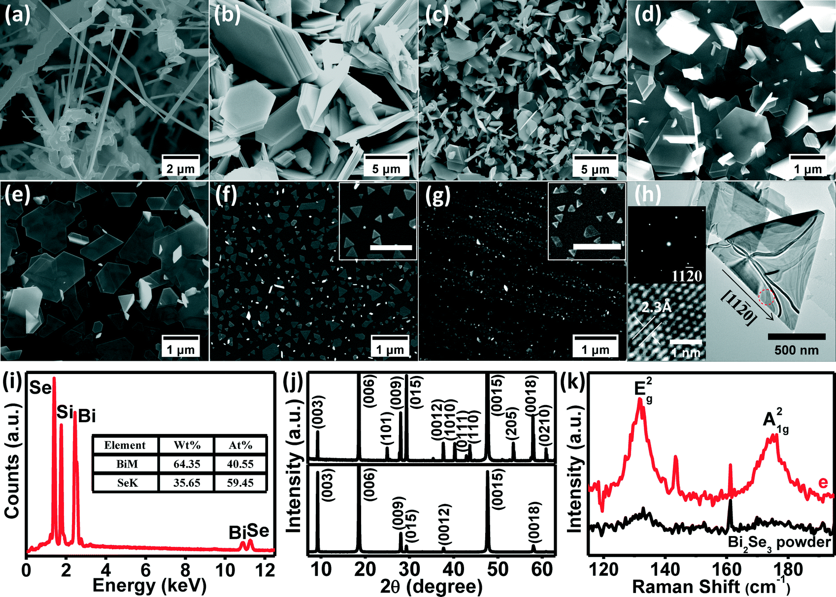 | ||
| Fig. 3 SEM images of Bi2Se3 nanomaterials synthesized by the VS mode. (a) Nanowires grown at 540 °C. (b–g) Bi2Se3 nanoplates grown at 524, 510, 490, 460, 440 and 415 °C, respectively. The scale bars of the insets are 500 nm. (h) TEM images of Bi2Se3 nanoplates. The insets are the corresponding HRTEM image and SAED patterns taken at the red circle. (i) EDAX analysis of the Bi2Se3 nanostructures. (j) θ–2θ scan X-ray diffraction of the samples grown at 524 °C (upper curves) and 460 °C (lower curves), respectively. (k) Raman spectra of the samples grown at 460 °C and bulk Bi2Se3 powder, respectively. | ||
As shown in Fig. 3(b–g), when the substrate temperature is 524 °C or lower, the substrate surface was covered by well-faceted hexagonal and triangular NPs whose sizes and thicknesses decreased with decreasing temperature. In Fig. 3(b), a large number of hexagonal Bi2Se3 NPs with a smooth surface and clear steps can be observed. The presence of steps indicates that the Bi2Se3 NPs were formed by layer-on-layer growth. When the temperature is 490 °C, the orientation of the NPs is uniform with the hexagonal planes parallel to the substrate surface, as shown in Fig. 3(d). As the substrate temperature continues to decrease, the size of NPs shrinks and the shape of NPs changes from hexagonal to polygonal (as shown in Fig. 3(e)). When the substrate temperature is 440 °C or lower, only the triangular Bi2Se3 NPs with a size of several tens of nanometers are observed, as shown in Fig. 3(f) and (g). To confirm the microstructure of the synthesized Bi2Se3 nanostructures, some features shown in Fig. 3(e) were transferred to a copper grid for TEM measurements. As shown in Fig. 3(h), an equilateral triangle-shaped NP with straight edges can be observed. The corresponding selected-area electron diffraction (SAED) pattern and the high resolution TEM (HRTEM) image taken at the red circle are shown as insets in Fig. 3(h). The spotty SAED pattern and the clear lattice fringes indicate that the NP has single crystal nature with each edge parallel to the <110> direction.
From the thermodynamic point of view, the anisotropic morphologies of nanostructures are determined by the relative surface energies of various crystal planes. The facets with lower surface energies will be favored and mostly exposed. As reported by Yan and his coworkers,21 among the three low index planes {0001}, {10![[1 with combining macron]](https://www.rsc.org/images/entities/char_0031_0304.gif) 0} and {110} of rhombohedral Bi2Se3, {0001} planes have the lowest surface energy (i.e. Gibbs free energy), resulting in the 2D morphology of Bi2Se3. Meanwhile, {100} planes have a lower surface energy than {110} planes. Therefore, we can conclude that the exposed facets of the triangular NP in Fig. 3(h) must belong to the {100} planes of Bi2Se3.
0} and {110} of rhombohedral Bi2Se3, {0001} planes have the lowest surface energy (i.e. Gibbs free energy), resulting in the 2D morphology of Bi2Se3. Meanwhile, {100} planes have a lower surface energy than {110} planes. Therefore, we can conclude that the exposed facets of the triangular NP in Fig. 3(h) must belong to the {100} planes of Bi2Se3.
Fig. 3(i) shows the EDAX analysis of the Bi2Se3 nanostructures. The average Bi/Se atomic ratio of the samples grown at different temperatures is 2.03/2.97, indicating that the Bi2Se3 nanostructures are very close to the stoichiometry. The large yield of materials allows us to collect enough materials for XRD measurements. The XRD measurements were conducted in a conventional θ/2θ scan type. The upper and lower curves in Fig. 3(j) show the corresponding XRD patterns of the samples shown in Fig. 3(b) and (e), respectively. All of the diffraction peaks match well with the standard data of the rhombohedral Bi2Se3. The full-width at half-maximum (FWHM) of the (006) peaks is only 0.17°, indicating that Bi2Se3 nanostructures grown by the VS mechanism have excellent crystallinity. It is noteworthy that only the c-axis diffraction peaks can be observed in the θ/2θ scan for the sample presented in Fig. 3(e). Therefore, it can be concluded that the Bi2Se3 NPs in Fig. 3(e) grow preferentially along the in-plane directions with their c-axes perpendicular to the substrate surface.
Raman scattering measurements were carried out using a micro-Raman spectroscopy system with a 488 nm laser as excitation source. In Fig. 3(k), the red and black curves correspond to the Raman spectra of the same sample as in Fig. 3(e) and the bulk Bi2Se3 powder, respectively. Two characteristic peaks at ~131 cm−1 and ~175 cm−1 correspond to the in-plane (Eg2) and the out-of-plane vibration mode (A1g2) of the rhombohedral Bi2Se3 lattice, respectively, whose intensities are reported to be very sensitive to the thickness of NPs.22 As can be seen in Fig. 3(k), both Eg2 and A1g2 vibrations are significantly strong for the Bi2Se3 NPs in comparison with the bulk Bi2Se3 powder. Such kind enhancement of Raman vibrations had also been observed by others in Bi2Se3 and Bi2Te3 NPs with the thickness less than 16 QLs, which was tentatively ascribed to the Fabry–Perot interference.23
The growth of Bi2Se3 nanostructures was also carried out in the VLS growth mode. The growth conditions are the same as the VS growth except that an Au catalyst was used. In VLS growth, Au catalysts can accelerate the collection of raw materials and subsequently the growth rate of nanostructures.24,25Fig. 4(a–e) show the SEM images of the samples grown by VLS mode at 500, 440, 370, 340, and 250 °C, respectively. In Fig. 4(a), a large number of small hexagonal Bi2Se3 nanostructures can be observed on the substrate surface with Au nanoparticles located at the top of each hexagonal nanostructure. The diameters of the spherical Au nanoparticles are in the range of 100–600 nm. When the temperature is 440 °C, NWs and NRs with a length of up to a hundred microns were obtained, as shown in Fig. 4(b). For example, a 200 nm wide and over 100 μm long NW and a 1 micron wide and 30 micron long NR are shown in Fig. 4(f) and (g), respectively. On the tip of the NW and the NR, Au nanoparticles can be observed. Additionally, the widths of NWs or NRs increase with the increasing size of the Au nanoparticles, which is common for the VLS growth of nanostructures.26 The angle between the two straight edges of the NR shown in Fig. 4(g) is measured to be 120° which is consistent with the angle between the {110} planes of the rhombohedral Bi2Se3. In contrast to the smooth NW and NR shown in Fig. 4(f) and (g), another type of Bi2Se3 NW with clear steps and facets on its sidewall is shown in Fig. 4(h). EDAX analysis on the tip of the NW confirms that the hemispherical feature at the tip of the NW is made of Au. Such kind of faceted sidewalls has been widely observed on Si NW grown by the VLS mode.26–28 Xu et al. have attributed the formation of Si NWs with faceted sidewalls to the diffusion of tiny Au nanoparticles to the sidewalls as NWs growing along the long axis.29 Therefore, we would tentatively speculate that the same mechanism can be used to explicate the growth of the Bi2Se3 NW in Fig. 4(h). When the substrate temperature is 370 °C or lower, the surface of the substrates is covered by a large amount of Bi2Se3 NPs whose sizes decrease with decreasing temperature, as shown in Fig. 4(c–e). These NPs have flat and smooth surfaces. XRD patterns of the NPs are similar to the lower curve in Fig. 3(j), indicating that the c-axes of the NPs are also perpendicular to the substrate surface. In contrast to the VS growth implemented at the same temperature, small triangular Bi2Se3 NPs are rarely observed, but a few large Bi2Se3 NPs with a lateral dimension of up to 50 μm were obtained, as shown in Fig. 4(i). The morphological difference between the VLS and the VS growth is probably due to the higher growth rate of the nanostructures in the VLS mode than in the VS mode. Fig. 4(j) shows the TEM image of a Bi2Se3 NR similar to the NR in Fig. 4(g). The corresponding HRTEM image and SAED patterns taken at the red circle are presented as insets. The clear and indexed hexagonal SAED patterns reveal that the NR has single crystalline nature and grows preferentially along the <110> direction. The lattice spacing is calculated to be 2.3 Å which is consistent with the d-space of (110) planes of the rhombohedral Bi2Se3.
 | ||
| Fig. 4 SEM images of Bi2Se3 nanomaterials synthesized by the VLS mode. (a) Hexagonal structures grown at 500 °C. (b) Bi2Se3 nanowires grown at 440 °C. (c–e) Bi2Se3 nanoplates grown at 370, 340 and 250 °C, respectively. The scale bars of the insets are 1 μm. (f) A nanowire grown along the c-axis. (g) A sheet-like wide nanoribbon; the angle between the two straight edges of the nanoribbon is 120°. (h) A nanowire is formed by stacking of nanoplates. (i) A large nanoplate. (j) TEM image of a Bi2Se3 nanoribbon. The insets are the corresponding HRTEM image and SAED patterns taken at the red circle. | ||
The formation of various Bi2Se3 nanostructures by the VS and the VLS growth modes can be discussed from the thermodynamic point of view. As discussed before, {0001} and {110} planes of Bi2Se3 have the lowest and highest surface energies, respectively. When the substrates were placed at the high temperature zone where is close to the Bi2Se3 powders, high supersaturated BiSe and Se2 vapor resulted in the high growth rate of nanostructures. Therefore, a large amount of nanostructures with various shapes like ribbons, zigzag, diamond and polygon can be observed for the VS growth, as shown in Fig. 3(a). As the substrate temperature and the BiSe and Se2 vapor pressure decreased, the growth rate decreased correspondingly. The surface adsorbed molecules will have more time to migrate on the low energy surface, resulting in the lateral growth of Bi2Se3 NPs along the in-plane directions. Therefore, we can see the formation of a lot of micron to nanometer-sized hexagonal Bi2Se3 NPs with decreasing substrate temperature in the VS growth mode, as shown in Fig. 3(b–g).
However, the situation will be different for the VLS growth mode. If the substrate temperature is higher than 500 °C, most of the adsorbed vapor molecules re-evaporated away from the substrate surface except at the site of the Au particles. As a result, only small and low density hexagonal plates can be observed, as shown in Fig. 4(a). With a decrease in substrate temperature, the molecule re-evaporation rate decreased and a large dimensional structure emerged. When the substrate temperature is lower than 500 °C, a large number of Bi2Se3 NRs were formed due to the lower reaction energy at the interface between the liquid Au catalyst and Bi2Se3, as shown in Fig. 4(b). The formation of NRs with (100) edges and (0001) top surfaces is energetically favorable from the thermodynamic point of view. Once the substrate temperature is lower than 440 °C, the preferential growth along the <110> direction was replaced by the random growth along diverse directions, which is probably due to the substrate temperature being below the eutectic temperature of the catalyst alloy.
It is noteworthy that some novel bridge-like nanostructures consisting of two NRs and one NP can be observed when the substrate temperature is in the range of 440–450 °C. Fig. 5(a) and (b) show the SEM image of a typical bridge-like nanostructure and the TEM image of another one, respectively. In order to compare the lattice constants and the orientations of the NR and the NP, SAED and HRTEM measurements were conducted at the two red circles in Fig. 5(b). The electron diffraction patterns and lattice fringes remained unchanged when the electron beam shifted between these two spots, revealing that the NP and the NR have the same crystalline structure and orientation.
 | ||
| Fig. 5 (a) Typical bridge-like Bi2Se3 nanostructure that consists of two nanoribbons and a nanoplate. (b) TEM image of a bridge-like Bi2Se3 nanostructure. The insets are the corresponding HRTEM image and SAED patterns taken at the red circles. | ||
From a survey of the SEM images, we also notice that a large number of Bi2Se3 NRs and NPs were formed at high and low temperature zones, respectively. On the contrary, bridge-like nanostructures are rare and only appear at a specific medium temperature zone. In addition, most of the bridge-like nanostructures are suspended in midair with the NRs attaching to the substrate. Therefore, it is reasonable to speculate that the formation of the bridge-like nanostructures originates from the epitaxial growth of NPs on the sidewalls of NRs along one of the <110> directions. In order to obtain more bridge-like nanostructures with large dimensions, we developed a two-step growth process in which NWs and NRs were utilized as the nucleation centers and templates for the subsequent lateral growth of NPs. The details of the two-step growth process can be briefly addressed as follows. Firstly, Bi2Se3 NWs and NRs were fabricated by the VLS growth at 475 °C for 120 minutes, and then the growth was paused. Secondly, the substrates were shifted 1 centimeter towards the downstream side where the temperature was 460 °C. Then the growth was resumed for 120 minutes. The Ar flow rate was kept at 65 sccm during the first and second step growth processes.
Fig. 6(a) and (b) show SEM images taken at the same area before and after the second step growth, respectively. As can be seen in Fig. 6(c), some NWs with a length of up to one hundred microns can be observed after the first growth. After the second growth, many bridge-like nanostructures with a lateral dimension larger than 30 microns are observed, as shown in Fig. 6(d). A survey on the average size and the number of the bridge-like Bi2Se3 nanoplates has been done, which shows that the average size of bridge-like structures increased from 8 μm2 for the conventional growth to 13.4 μm2 for the two-step growth. More importantly, by employing the two-step growth, the number of Bi2Se3 bridges with the size larger than 30 μm2 nearly increased by twenty times.
 | ||
| Fig. 6 (a and b) SEM images of Bi2Se3 nanostructures after the first growth process and the secondary growth process, respectively. (c and d) The corresponding zoom-in SEM images in (a) and (b), respectively. | ||
The formation of bridge-like structures in the two-step growth can be understood by simply combining the VLS and the VS growth mechanisms discussed above. Briefly speaking, the contribution of the long Bi2Se3 NRs to the formation of Bi2Se3 bridges in the second step VS growth can be summarized in two aspects. First, the long NRs can offer more nucleation sites on their (100) edges, which can facilitate the in-plane growth of the bridge deck. Second, the NRs will work as the original templates which limit the width and even the thickness of bridges.
To further prove our assumption about the formation of bridge-like Bi2Se3 nanostructures, five NRs were mechanically transferred by using a micro-probe station from the firstly grown sample onto a clean SiO2 substrate, as shown in Fig. 7(a). Then, the five NRs on the clean SiO2 substrate were placed into the furnace for the secondary growth under the same conditions mentioned above. Fig. 7(b) and (c) show the surface morphology after the secondary growth by optical microscopy and SEM, respectively. It can be seen that after the secondary growth the lateral dimensions of the NRs increase significantly from half or one micron to ten microns, while the heights of the NRs increase from 50–100 nm to ~1 micron which is estimated by the defocus effects of the optical microscopy. However, for the central NR among the five NRs there are two positions where the width and the height did not change significantly. We labeled the two positions as 1 and 2 in Fig. 7(b) and (c). The zoom-in optical microscopy and SEM images at positions 1 and 2 are shown in Fig. 7(b1–b2) and (c1–c2). At position 1, multiple steps of NPs with clear facets are connected by a narrow NR whose width is almost unchanged after the second growth. Obviously, these micron-sized NPs have been extending from the narrow NR with the upper NPs constraining to the bottom ones. At position 2, a NP with uneven armchair-like edges is attached to the arc-shape NR. The contrast variation at the downside of the NP in Fig. 7(c2) originates from the variation of thickness and will be discussed later. Additionally, the angles between adjacent straight edges of the NPs shown in Fig. 7(c1) and (c2) are about 120°, which indicates that the top surface of the NPs and the NR is the {0001} plane of Bi2Se3, while the facets are the more stable {100} planes.
 | ||
| Fig. 7 (a) Optical microscopy image of five nanoribbons, transferred mechanically for the first growth sample by a micro-probe. (b and c) Optical microscopy and SEM images of the five nanoribbons after the secondary growth, respectively. (b1 and b2) The zoom-in optical microscopy images taken at positions 1 and 2 in (b), respectively. (c1 and c2) The zoom-in SEM images taken at positions 1 and 2 in (c), respectively. (d and e) AFM images taken at positions 1 and 2, respectively. The thickness profiles were taken at the white dashed lines, correspondingly. | ||
Fig. 7(d) and (e) show the AFM images taken at positions 1 and 2, respectively. In Fig. 7(d), the uniform color contrast reveals that the top surfaces of the Bi2Se3 NPs and NR are atomic smooth. The height profile along the white dashed line shows that the vertical and horizontal dimensions of the NR are 64 nm and 480 nm, respectively, while the step heights of the stacking NPs vary from several to tens of nanometers randomly, suggesting that the Bi2Se3 NPs are formed by layer-by-layer growth. In Fig. 7(e), the height profile along the white dashed line II shows that the height and the width of the NR are the same as that of the NR shown in Fig. 7(d). However, the height profile along the white dashed line I shows that the height of the NP is uneven along the radial and the axial directions of the NR. The NP is 64 nm thick at the near NR side and becomes thinner and thinner as the NP extended to the far-end side. However, the reason for the nonuniformity of height and width is not clear now. We tentatively ascribe it to the arc shape of the NR at position 2 in Fig. 7, because bending of the NR might induce compressive strain accumulation and an uneven growth rate in the Bi2Se3 NP. However, no exact explanation for the nonuniform growth rate at different portions of the single NR can be provided at this point. Further studies have to be done to clarify the issue.
Conclusions
In summary, we report the syntheses of various Bi2Se3 nanostructures such as nanoribbons, nanoplates and bridge-like nanostructures by the VS and VLS growth mechanisms. Bi2Se3 nanoribbons with the growth normal along <110> directions are mostly formed at the high temperature zone. On the other hand, Bi2Se3 nanoplates with their c-axes perpendicular to the substrate surface are mainly formed by layer-by-layer growth at the low temperature zone. Meanwhile, novel bridge-like nanostructures generally consisting of two nanoribbons and one nanoplate are occasionally observed in a very narrow temperature window in the medium-temperature zone. In order to obtain more bridge-like nanostructures with large dimensions, a two-step growth process has been developed to increase the number and the dimensions of the bridge-like Bi2Se3 nanostructures, which provide an effective route for fabricating large-size layered Bi2Se3 nanostructures and could benefit the fundamental research studies and the optoelectronic and spintronic applications of topological insulators. The formation mechanism of various nanostructures was also discussed from the thermodynamic point of view.
Acknowledgements
This work is supported by the NSFC (No. 51172041, 51202026, 91233204, 51372035, 51422201 and 11204029), the 973 Program (No. 2012CB933703), the “111” Project (No. B13013), the Fund from Jilin Province (No. 20121802, 201201061, 20140309012GX and 20140201008GX), the Doctoral Fund of Ministry of Education of China (No. 20110043120004), the Fundamental Research Funds for the Central Universities (No. 2412015BJ003) and SKLLIM1404.References
- V. Nicolosi, M. Chhowalla, M. G. Kanatzidis, M. S. Strano and J. N. Coleman, Science, 2013, 340, 1419 CrossRef.
- F. Bonaccorso, L. Colombo, G. Yu, M. Stoller, V. Tozzini, A. C. Ferrari, R. S. Ruoff and V. Pellegrini, Science, 2015, 347, 41 CrossRef CAS PubMed.
- X. Huang, C. Tan, Z. Yin and H. Zhang, Adv. Mater., 2014, 26, 1 CrossRef PubMed.
- D. Kong, J. C. Randel, H. Peng, J. J. Cha, S. Meister, K. Lai, Y. Chen, Z.-X. Shen, H. C. Manoharan and Y. Cui, Nano Lett., 2010, 10, 329–333 CrossRef CAS PubMed.
- W. Dang, H. Peng, H. Li, P. Wang and Z. Liu, Nano Lett., 2010, 10, 2870–2876 CrossRef CAS PubMed.
- H. Lind, S. Lidin and U. Häussermann, Phys. Rev. B: Condens. Matter Mater. Phys., 2005, 72, 184101 CrossRef.
- K. M. F. Shahil, M. Z. Hossain, V. Goyal and A. A. Balandin, J. Appl. Phys., 2012, 111, 054305 CrossRef PubMed.
- K. S. Novoselov, A. K. Geim, S. V. Morozov, D. Jiang, Y. Zhang, S. V. Dubonos, I. V. Grigorieva and A. A. Firsov, Science, 2004, 306, 666–669 CrossRef CAS PubMed.
- M. Qian, Y. S. Zhou, Y. Gao, J. B. Park, T. Feng, S. M. Huang, Z. Sun, L. Jiang and Y. F. Lu, Appl. Phys. Lett., 2011, 98, 173108 CrossRef PubMed.
- H. Cui, H. Liu, J. Wang, X. Li, F. Han and R. I. Boughton, J. Cryst. Growth, 2004, 271, 456–461 CrossRef CAS PubMed.
- G. Zhang, W. Wang, X. Lu and X. Li, Cryst. Growth Des., 2009, 9, 145–150 CAS.
- Y.-F. Lin, H.-W. Chang, S.-Y. Lu and C. W. Liu, J. Phys. Chem. C, 2007, 111, 18538–18544 CAS.
- Y. Zhang, K. He, C.-Z. Chang, C.-L. Song, L.-L. Wang, X. Chen, J.-F. Jia, Z. Fang, X. Dai, W.-Y. Shan, S.-Q. Shen, Q. Niu, X.-L. Qi, S.-C. Zhang, X.-C. Ma and Q.-K. Xue, Nat. Phys., 2010, 6, 584–588 CrossRef PubMed.
- S. Wu, C. Huang, G. Aivazian, J. S. Ross, D. H. Cobden and X. Xu, ACS Nano, 2013, 7, 2768–2772 CrossRef CAS PubMed.
- M. Saghir, M. R. Lees, S. J. York and G. Balakrishnan, Cryst. Growth Des., 2014, 14, 2009–2013 CAS.
- J. J. Cha, K. J. Koski and Y. Cui, Phys. Status Solidi RRL, 2012, 1–11 CAS.
- F. C. Frank, Discuss. Faraday Soc., 1949, 5, 48–54 RSC.
- F. C. Frank, S. P. F. Humphreys-Owen, I. N. Stranski, H. K. Hardy, W. K. Burton, N. Cabrera, R. S. Bradley, J. L. Amoròs, C. W. Bunn and U. R. Evans, Discuss. Faraday Soc., 1949, 5, 66–79 RSC.
- M. H. R. J. Plusjé, W. J. Dunning, W. K. Burton, N. Cabrera, R. F. Strickland-Constable, S. Fordham, F. C. Frank, W. E. Garner, K. G. Denbigh, W. A. Wooster, D. R. Hale, A. Juliard, A. E. Robinson, L. J. Griffin, I. N. Stranski, C. W. Bunn, Y. Haven, E. O. Hall, H. K. Hardy, H. E. E. Powers, A. F. Wells, A. R. Ubbelohde and J. L. Jones, Discuss. Faraday Soc., 1949, 5, 183–197 RSC.
- F. C. Frank, Adv. Phys., 1952, 1, 91–109 CrossRef PubMed.
- Y. Yan, Z.-M. Liao, Y.-B. Zhou, H.-C. Wu, Y.-Q. Bie, J.-J. Chen, J. Meng, X.-S. Wu and D.-P. Yu, Sci. Rep., 2013, 3, 1 Search PubMed.
- J. Zhang, Z. Peng, A. Soni, Y. Zhao, Y. Xiong, B. Peng, J. Wang, M. S. Dresselhaus and Q. Xiong, Nano Lett., 2011, 11, 2407–2414 CrossRef CAS PubMed.
- S. Y. F. Zhao, C. Beekman, L. J. Sandilands, J. E. J. Bashucky, D. Kwok, N. Lee, A. D. LaForge, S. W. Cheong and K. S. Burch, Appl. Phys. Lett., 2011, 98, 141911 CrossRef PubMed.
- R. S. Wagner and W. C. Ellis, Appl. Phys. Lett., 1964, 4, 89 CrossRef CAS PubMed.
- R. S. Wagner, in Whisker Technology, ed. A. P. Levitt, Wiley-Interscience, New York, 1970, pp. 47–119 Search PubMed.
- J. B. Hannon, S. Kodambaka, F. M. Ross and R. M. Tromp, Nature, 2006, 440, 69–71 CrossRef CAS PubMed.
- M. I. Hertog, J.-L. Rouviere, F. Dhalluin, P. J. Desre, P. Gentile, P. Ferret, F. Oehler and T. Baron, Nano Lett., 2008, 8, 1544–1550 CrossRef PubMed.
- T. Kawashima, T. Mizutani, T. Nakagawa, H. Torii, T. Saitoh, K. Komori and M. Fujii, Nano Lett., 2008, 8, 362–368 CrossRef CAS PubMed.
- T. Xu, J. P. Nys, A. Addad, O. I. Lebedev, A. Urbieta, B. Salhi, M. Berthe, B. Grandidier and D. Stiévenard, Phys. Rev. B: Condens. Matter Mater. Phys., 2010, 81, 115403 CrossRef.
| This journal is © The Royal Society of Chemistry 2015 |