
 Open Access Article
 This Open Access Article is licensed under a Creative Commons Attribution-Non Commercial 3.0 Unported Licence
Role of catalyst in controlling the growth and morphology of one-dimensional SiC nanostructures†
Lei
Zhang
ab,
Hao
Zhuang
a,
Chun-Lin
Jia
b and
Xin
Jiang
*a
aInstitute of Materials Engineering, University of Siegen, Paul-Bonatz-Str. 9-11, 57076 Siegen, Germany. E-mail: xin.jiang@uni-siegen.de; Fax: + 49 271 740 2442; Tel: +49 271 740 2966
bPeter Grünberg Institute and Ernst Ruska-Centre for Microscopy and Spectroscopy with Electrons, Forschungszentrum Jülich GmbH, 52425 Jülich, Germany
First published on 10th August 2015
Abstract
To control the morphologies of one-dimensional (1D) nanostructures, especially during the catalyst-assisted growth of semiconductor nanostructures, is the key to unlock their potential applications. In this work, we demonstrate that, the morphology of the 1D silicon carbide (SiC) nanostructures can be controlled by manipulating the composition of the catalyst in the microwave plasma chemical vapor deposition process. It is revealed that iron silicide presents as the main catalyst to initiate the growth of 1D SiC nanostructure. High-resolution transmission electron microscopic analysis shows that, the stoichiometry of the iron silicide governs the final morphology of 1D SiC nanowire. For the growth of SiC nanowires, the catalyst is Fe5Si3, while it is Fe3Si for SiC nanoneedles. A special orientation match between the iron silicide catalyst and the SiC nanowire is observed for the first time during the growth of SiC nanostructures. The mechanism for the different morphology of the SiC nanostructures is believed to be the different etching resistivity of the catalyst particles under H2 plasma etching. Based on the above mechanism, a continuous change in the morphology of the SiC nanostructures has been achieved by controlling the supply of Si during growth.
1. Introduction
One-dimensional (1D) nanostructures have attracted intensive research attention due to their unique properties and potential applications in nanoscale devices.1,2 Over the past decades, catalyst-assisted growth of various 1D semiconductor nanostructures has been well developed.3–6 During this time, it has been an important concern to effectively control the morphology (i.e., shape, geometry, size, etc.) of the nanostructure during synthesis, as it could possibly influence the properties as well as the final performances of the nanostructures.7 In this context, dedicated research efforts have been paid to understanding their growth mechanism. Growth models, i.e., vapor–liquid–solid (VLS),8 vapor–solid–solid (VSS),9 and solid–liquid–solid (SLS),10etc., have been well developed to help direct the growth of the nanowires, especially nanowires of elemental semiconductors. It is widely accepted that, before the formation of a nanowire, a supersaturated liquid-state (VLS) or solid-state (VSS) catalyst alloy forms. Precipitation occurs at one side of the catalyst, which leads to the nucleation and continuous growth of the nanowire.11 Comparing to the VLS growth process, the catalyst, especially its orientation, is more decisive in determining the growth behavior of the nanowires in the VSS process. For example, an orientation match in the lattice between the nanowire and the catalyst has been already observed during the growth of Si, Ge, ZnO, GaAs, InP, etc. nanowires.6,12–16 It is known that the crystal structure and composition of the catalyst influence its orientation. Therefore, a binary phase diagram has been widely referred to while discussing the possible growth mechanism.17,18 Such a growth process, however, becomes more complicated while concerning the growth of compound semiconductor (groups III–V, IV–IV, II–VI semiconductors) nanowires, owing to the involvement of multiple precursors. Even though the importance of the composition and orientation of the catalyst has been already recognized, however, their actual influence on the growth behavior of the nanowires is still under debate and remains unclear.19 In this study, using an example of Fe-catalyzed growth of 1D SiC nanostructures, we demonstrate the impact of crystallographic structure of the metal alloy catalyst on the growth behavior of the nanostructures. Consequently, SiC nanowires and SiC nanoneedles are obtained by varying the composition of the catalyst. A special orientation match between the catalyst and the nanowire is observed. It should be noticed that, though intensive researches have been already carried out in the synthesis of SiC nanowires with different morphologies,20–25 and there were also some works about controlling the morphologies of the SiC nanostructures achieved by tuning the pressure of the source species26 or the growth temperature,27,28 this is the first direct observation of the orientation dependence between the SiC nanowire and the catalyst. Here, we choose SiC also because of its great technological importance. It is an important member in the group IV–IV wide band gap semiconductors29,30 and is believed to be a promising candidate for next generation of nano-electrical and optical devices, which could operate in the high temperatures, high power, and high frequency environments.31–362. Experimental section
In our previous investigations,37 SiC nanocables were obtained in the microwave plasma chemical vapor deposition (MWCVD) process using SiO2 plate as silicon source and CH4 as carbon source, respectively. Following the same strategy, in the present study, Fe coated p-type (001) Si wafer was used as the substrate and SiO2 plate was placed beside the wafer serving as the Si source in the MWCVD process. The iron film was sputtered on the Si wafer by a sputter coater (Polaron SC500). The sputtering was carried out at a current of 30 mA for 4 min. The Si substrate was used as received. The native oxide is not removed from the substrate. The thickness of the metal layer is 2–5 nm. The growth of the nanostructures was carried out at a constant gas pressure of 50 Torr and a microwave power of 2000 W. H2 and CH4 were used as the reactive gases for the deposition. During growth, pure hydrogen plasma etching was firstly carried out at 800–900 °C for 10 min. Afterwards, 5.5 sccm of CH4 was introduced into the chamber for the growth of the SiC nanostructures and the total growth time was 6 hours. The substrate temperature was measured by an optical pyrometer to be 800–900 °C. The morphology of the as-grown materials was investigated by scanning electron microscope (SEM) (Zeiss Ultra 55). In order to obtain the structural information of the catalyst, the SiC nanostructures were then removed from the substrate and put on a holy carbon coated copper grid for further characterization by transmission electron microscope (TEM) (FEI Tecnai G2 F20 and FEI Titan 80-300). Since the size and amount of the nanostructures are too small, it is almost impossible to obtain the information about them using X-ray diffraction (XRD) and Fourier transform infrared spectroscopy (FTIR) technique. In this context, we didn't include the XRD and FTIR results in the manuscript. Moreover, high-resolution TEM (HRTEM) images as well as the corresponding fast Fourier transformation (FFT) pattern focuses on a smaller area of the catalyst, which, we believe, is accurate and sufficient to address the crystallographic information of the catalyst. Therefore, we mainly focus on the HRTEM analysis of our catalyst.3. Results and discussion
Fig. 1(a) represents the SEM image of the typical overall morphology of the SiC nanostructures. It can be seen that dense nanostructures with a length of several micrometers have been obtained. The high magnification SEM image shown in Fig. 1(b) reveals that both straight and curved nanowires present and are randomly distributed. In addition to the nanowires, nanoneedles are also observed (Fig. 1(c)) with a lower density in comparison with the nanowires. In order to obtain more detailed structural information of the nanowires and nanoneedles, TEM analysis was carried out and the results are shown in Fig. 1(d–f). Fig. 1(d) presents the overall morphology of a SiC nanowire. It can be observed that the nanowire features a length of ~3 μm and a diameter of ~70 nm. Its diameter is almost constant along the length. Such a morphology matches well with the SiC nanowires observed in Fig. 1(b). Apparently, shorter and thinner nanowire also exists, as shown in Fig. S1(a) in ESI.† For all the nanowires observed, a cylindrical catalyst locates at the tip of the nanowires, indicating the nanowires have a tip-growth nature.20,24 It is also noteworthy that the diameter of the catalyst is slightly larger than that of the nanowire (this is more apparent in the following TEM images, see Fig. 2). Fig. 1(e) shows the typical morphology of a SiC nanoneedle, whose length is ~700 nm. It is much shorter than the ones observed in Fig. 1(c). This might be due to the unavoidable rupture of the nanoneedles during the sample preparation process (i.e. high energy sonication). It can be observed that the diameter of the nanoneedle decreases significantly from ~30 nm at the bottom to ~6 nm at the tip. A spherical catalyst particle is also observed at the tip, showing the tip-growth nature, too. In addition to the straight nanoneedles, slightly curved nanoneedles can also be found (see Fig. S1(b) in ESI†). Moreover, stripe-patterns of diffraction contrast are clearly observable in both of the nanowires and nanoneedles (Fig. S1†), indicating the existence of a high density of planar defects. Fig. 1(f) shows the HRTEM image of one nanowire. Perpendicular to the longitudinal axial direction (the growth direction of the SiC nanowire), the lattice spacing is measured to be 0.252 nm, which agrees well with the interplanar spacing of the close-packed planes in SiC (i.e., {111} planes in 3C-SiC (ICDD PDF# 29-1129) or {0001} planes in the 2H-SiC (ICDD PDF# 29-1130)). Therefore, the growth direction of the SiC nanowires is along the normal of the close-packed planes, which is in good accordance with previously reported results.31,34,35,38 Since the growth of the nanowire is a layer-by-layer stacking of the close-packed planes, according to different atomic stacking sequences, 3C-SiC (ABCABC…) and 2H-SiC (ABAB…) segments were formed, which are marked as “3C” and “2H” in Fig. 1(f), respectively. Here, A, B, C represents the three possible stacking positions for the close-packed planes. Meanwhile, when some disordered stacking sequence occurs, nanotwins (marked as “T”) and stacking faults (marked as “SF”) were thus observed in the SiC nanowires. These planar defects are also observed in the SiC nanowires fabricated using other strategies owing to their low formation energy.23,31,34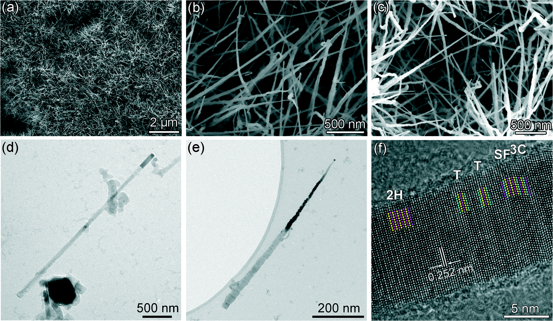 | ||
| Fig. 1 (a–c) SEM images of the SiC nanostructures: (a) over-view image, (b) high magnification image showing SiC nanowires, and (c) high magnification image showing SiC nanoneedles; (d–f) TEM images of the SiC nanostructures: (d) nanowire, (e) nanoneedle, (f) HRTEM image of structural variety of SiC and planar defects in a nanostructure. | ||
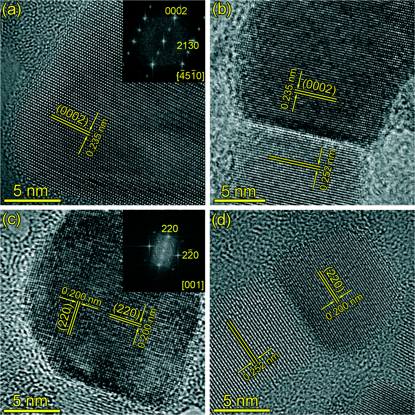 | ||
| Fig. 2 (a, b) HRTEM images of the catalyst of the SiC nanowires, and (c, d) HRTEM images of the catalyst of the SiC nanoneedles. | ||
From the above observation, it is clear that both nanowires and nanoneedles show a tip-growth nature. Since both of these nanostructures grow simultaneously, their growth atmosphere should be identical. Therefore, it is reasonable to expect that the driving force in the different morphologies of these nanostructures lay in the differences in catalysts. In this context, HRTEM analysis of the catalyst was carried out and the results are shown in Fig. 2. Fig. 2(a) and (b) show the HRTEM images of the catalysts of two nanowires with different diameters. FFT of Fig. 2(a) (see inset) depicts the typical lattice fringes of single crystalline Fe5Si3 (ICDD PDF# 38-0438), indicating the composition of catalyst is Fe5Si3. Even though different diameters of the catalysts are observed (~60 nm for Fig. 2(a) and ~13 nm for Fig. 2(b)), the catalysts show the same crystal structure with lattice fringe spacing of 0.235 nm, which agrees with the interplanar spacing of Fe5Si3 {0002} planes. Moreover, energy-dispersive X-ray spectroscopy (EDS) result also confirms the presence of Fe and Si in the catalyst particle (see Fig. S2 in ESI†). Fig. 2(c) and (d) show the HRTEM images of the catalysts at the tip of two SiC nanoneedles with different sizes. The two catalyst crystals show spherical shape with diameters of ~15 nm and ~10 nm, respectively. The EDS result indicates the co-existence of Fe and Si in the catalyst (see Fig. S2 in ESI†). The lattice fringes of both catalysts match well with the interplanar distance of the {220} planes of Fe3Si crystal (ICDD PDF# 45-1207), indicating the composition of the catalyst is Fe3Si. This is further confirmed by the FFT pattern of Fig. 2(c) (shown in the inset), which clearly depicts the lattice fringes of single crystalline Fe3Si.
It is also clearly seen from Fig. 2(b) and (d) that certain orientation dependence between the catalyst and the nanostructure exists. The close-packed planes of the SiC nanostructures ({111} planes of 3C-SiC crystal or {0001} planes of the 2H-SiC crystal, both of their interplanar distances are 0.252 nm) are parallel to the {0002} planes of Fe5Si3 for the nanowires and the {220} planes of Fe3Si for the nanoneedles, respectively. Such results imply a special crystallographic relationship between the SiC nanostructures and the catalysts.
To further confirm this, a more detailed investigation at the interface of the catalyst and the nanowire is carried out. Fig. 3(a) represents the overall HRTEM image of the interface between the SiC nanowire and the catalyst. Since only the (0002) planes of Fe5Si3 are active to catalyze the formation of the nanowires, other facets might act as the adsorption facets. Fig. 3(b) shows a magnified image of the framed area. The yellow lines indicate the (21![[3 with combining macron]](https://www.rsc.org/images/entities/char_0033_0304.gif) 1) planes of the Fe5Si3 crystal and the (11
1) planes of the Fe5Si3 crystal and the (11![[1 with combining macron]](https://www.rsc.org/images/entities/char_0031_0304.gif) ) planes of the 3C-SiC crystal, respectively. It can be seen that every five Fe5Si3 (211) planes match well with every four 3C-SiC (11) planes, which is in good accordance with the interplanar distances of the Fe5Si3 (211) plane (0.200 nm) and the 3C-SiC (11) plane (0.252 nm). The angle between the (211) plane and the (0002) plane is calculated to be 64.9° in Fe5Si3 crystal, while the angle between the (11) plane and the (111) plane is calculated to be 70.5° in 3C-SiC crystal. Since the (111) plane of the SiC nanowire is parallel to the (0002) plane of the Fe5Si3 catalyst, the angle between the 3C-SiC (11) plane and the Fe5Si3 (211) plane is about 5.6°, showing a mismatch. During the growth, the energy accumulated by such a mismatch can be possibly released by the continuous formation of planar defects, i.e. stacking faults and twins. As shown by the arrow in Fig. 3(b), a stacking fault can be readily observed near to the interface of the nanowire. The above phenomenon is even more obvious in Fig. 3(d), which is the HRTEM image of another nanowire. In this nanowire, a good orientation match between the (211) planes of Fe5Si3 and (11) planes of 3C-SiC can be clearly observed. As for the SiC nanoneedles, however, the direct evidence of such relationship cannot be observed owing to the quick damage of the interface during the imaging process. However, since the (111) plane of the nanoneedle is also parallel to the (220) plane of the Fe3Si crystal, it would be reasonable to consider that the nanoneedles might also exhibit a similar growth relationship to that of the nanowire.
) planes of the 3C-SiC crystal, respectively. It can be seen that every five Fe5Si3 (211) planes match well with every four 3C-SiC (11) planes, which is in good accordance with the interplanar distances of the Fe5Si3 (211) plane (0.200 nm) and the 3C-SiC (11) plane (0.252 nm). The angle between the (211) plane and the (0002) plane is calculated to be 64.9° in Fe5Si3 crystal, while the angle between the (11) plane and the (111) plane is calculated to be 70.5° in 3C-SiC crystal. Since the (111) plane of the SiC nanowire is parallel to the (0002) plane of the Fe5Si3 catalyst, the angle between the 3C-SiC (11) plane and the Fe5Si3 (211) plane is about 5.6°, showing a mismatch. During the growth, the energy accumulated by such a mismatch can be possibly released by the continuous formation of planar defects, i.e. stacking faults and twins. As shown by the arrow in Fig. 3(b), a stacking fault can be readily observed near to the interface of the nanowire. The above phenomenon is even more obvious in Fig. 3(d), which is the HRTEM image of another nanowire. In this nanowire, a good orientation match between the (211) planes of Fe5Si3 and (11) planes of 3C-SiC can be clearly observed. As for the SiC nanoneedles, however, the direct evidence of such relationship cannot be observed owing to the quick damage of the interface during the imaging process. However, since the (111) plane of the nanoneedle is also parallel to the (220) plane of the Fe3Si crystal, it would be reasonable to consider that the nanoneedles might also exhibit a similar growth relationship to that of the nanowire.
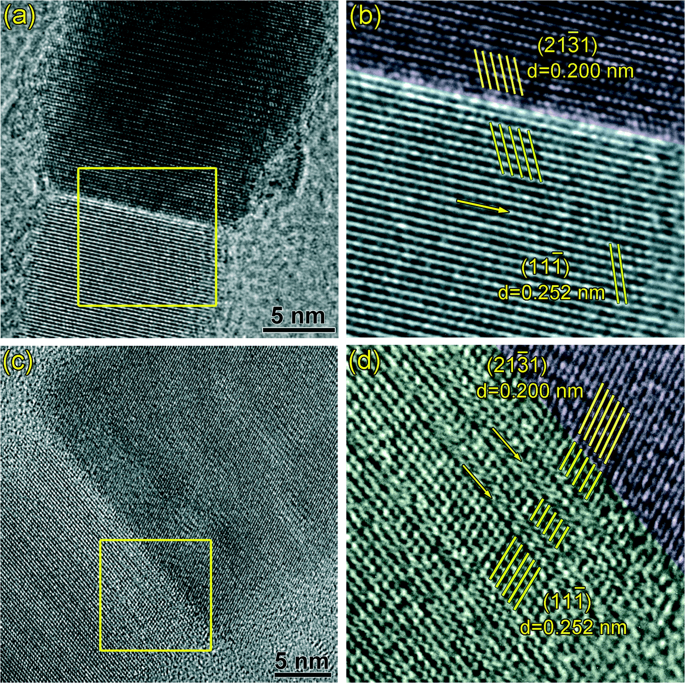 | ||
| Fig. 3 (a) and (c) HRTEM images of the interface between the SiC nanowire and the catalyst showing a special crystallographic relationship; (b) and (d) magnified images of the framed area of the (a) and (c), respectively. | ||
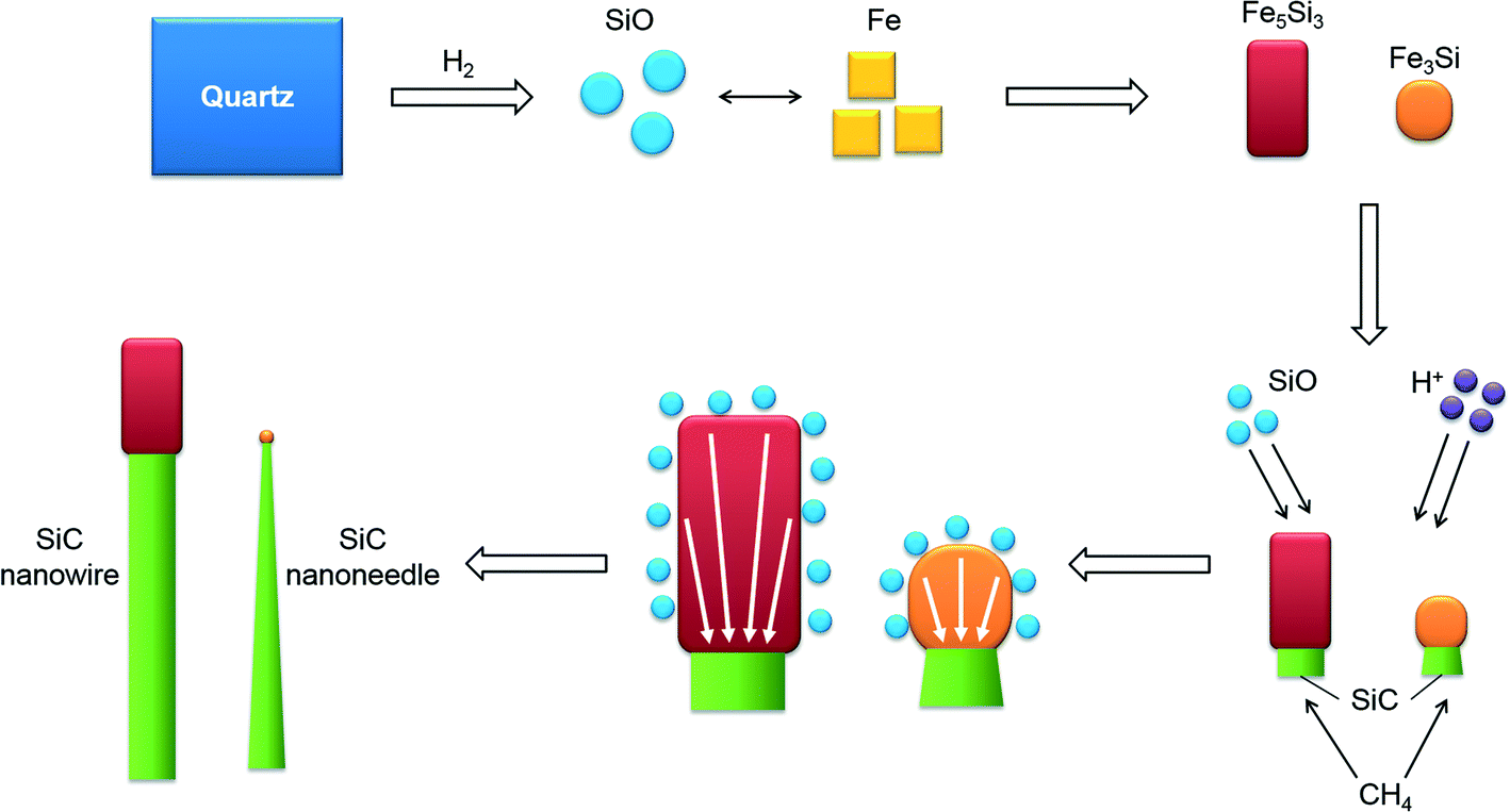
The above observation indicates that the SiC nanostructures grow with a special crystallographic relationship with the catalysts and the morphologies of the nanostructures (nanowires or nanoneedles) are dependent on the composition of their catalysts. Therefore, a natural question arises: what is the mechanism behind the above phenomena? Since catalyst alloys are formed during the process, the growth of the SiC nanostructures most likely follows the widely accepted VLS or VSS mechanism for the growth of various 1D nanostructures.3,9,11 Considering that under the present deposition condition (substrate temperature of 800–900 °C) the catalyst alloy is solid according to the Fe–Si phase diagram (see Fig. 4), the VSS growth mechanism plays the role in the present study. Moreover, a special crystallographic relationship exists between the catalyst and the nanostructure. This is also more common in the VSS growth process,12–16 which further indicates that the VSS growth mechanism is applicable in the present study. During the growth of the nanostructures, quartz (SiO2) was firstly reduced into gaseous SiO in the reductive atmosphere39,40 to supply Si precursors in the gas phase. At the beginning of the growth, Fe reacts with SiO to form iron silicide as catalyst during the H2 plasma etching process (10 min). Atomic force microscopy (AFM) surface topography images shows the dewetting effect after etching (see Fig. S3 in ESI†). When CH4 is introduced into the growth process, it started to react with the Si coming from the iron silicide to form the SiC nanostructure. The reaction prefers to occur on the (0002) plane of Fe5Si3 and (220) plane of Fe3Si to lower the total system energy. The orientation relationship between the nanostructure and the catalyst is thus maintained during growth, as shown in Fig. 3(b) and (d). When the nanostructure starts to grow, the Si concentration at the interface will decrease. As a result, a gradient in the Si concentration will be thus generated in the catalyst particle. Si started to diffuse from the area with high concentration to the interfacial area inside the catalyst to continuously supply the Si species for the growth of the nanostructures. Such a process leads to a decrease in the Si concentration in the catalyst. Therefore, the further dissolution of Si from the gas phase into the catalyst particle is also triggered (through the non-active facts), leading to the continuous growth of the SiC nanostructure.
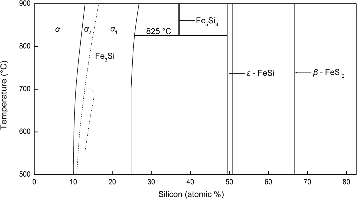 | ||
| Fig. 4 Binary phase diagram of Fe–Si.44 | ||
In addition to the orientation matching between the catalyst and the nanowire, it is also interesting to observe the different compositions of the catalysts leading the growth of the nanowires and nanoneedles. Since the two kinds of catalysts are both Fe–Si alloys and CH4 was introduced into this reaction, it is necessary to consider the influence of the carbon element on the formation of the Fe–Si alloys. Iron-based alloys have certain solubility towards carbon.41 Unfortunately, a detailed Fe–Si–C phase diagram in our region is not available in the literature. Upon a careful observation, we compared the interplanar distances of the catalyst lattices and FFT patterns with all the structures in ICDD PDF-2 database containing Fe, Si, and C. Fe5Si3 and Fe3Si are the only two structures that match well with the measurements. Therefore, we conclude the crystal structure of our catalysts to be Fe5Si3 and Fe3Si. Moreover, a theoretical study demonstrates that even C can dissolve into the Fe–Si compounds, it will not change the crystallographic structure of the compound but improve their structural stability.42 In this context, we believe our catalysts are Fe5Si3 and Fe3Si, and carbon might form solid solutions in the compounds with certain solubility.
Fe3Si, the catalyst leading to the growth of SiC nanoneedles, is an iron rich phase. As indicated by α1 and α2 in the Fe–Si phase diagram, the stoichiometric Fe3Si is thermodynamically the most stable form, even though it has a wide range of composition change, from 10–25 at% Si.43,44 In comparison with Fe3Si, Fe5Si3 is a Si rich phase according to the phase diagram. According to Kadečková et al.'s investigation,45 the chemical stability of the iron silicide increases with increasing Si ratio in the compound. Since the SiC nanostructures show a tip growth nature in the present study, the catalyst particles also underwent a strong etching by hydrogen plasma during the growth process. The lower chemical stability of Fe3Si leads to its lower etching resistivity, which in turn results in its continuous reduction in size with increasing growth time. Such a fact results in the decrease of the growth front area of the SiC nanostructures, forming SiC nanoneedles. In contrast, Fe5Si3 has much higher etching resistivity, which leads to its nearly unchanged size during the growth. As a result, SiC nanowire forms. It is also noted that the bottom size of the nanoneedles and nanowires are nearly similar (comparing Fig. 1(b) and (c)), indicating that the initially formed catalyst compounds are nearly the same in size. The size of the iron compound is determined by the initial size of iron particles. The homogeneous coating of iron onto the substrate before deposition enables a homogenous distribution of the size of iron catalyst on the substrate surface. The above growth process is summarized and schematically shown in Fig. 5.
 | ||
| Fig. 5 Schematic illustration of the growth mechanism. | ||
From the above discussion, it can be inferred that the compositions of the catalysts have a drastic influence on the morphology of the SiC nanostructures in the MWCVD process. The lower concentration of Si in the catalyst leads to the formation of nanoneedles and higher concentration of Si leads to the formation of nanowires. Such a phenomenon implies that the morphology of SiC nanostructures can be controlled by manipulating the supply of Si during the growth of the SiC nanostructures. Our proposed growth mechanism was further verified by the following experiment (Fig. 6(a)). A quartz plate is placed at the side of the iron coated Si wafer and serves as the Si source. During the process, Si containing species were etched from the quartz plate under hydrogen plasma and travels to the substrate for the growth of SiC nanostructures. Since the Si containing species only come from the quartz source, its content in the plasma decreases with increasing distance from the quartz plate. In this context, a gradient in the Si concentration is artificially created with high Si concentration near to the quartz and low Si concentration far away from the quartz. As a result, a continuous morphology change in the SiC nanostructures can be observed with increasing distance from the quartz plate. The growth of the SiC nanostructures started from the area whose distance to the quartz source is 3 mm. In the area near to the quartz (from 3 to 4 mm, Region I as noted in Fig. 6(a)), the surface of the substrate was covered by a very dense layer of SiC nanostructures, as shown in Fig. 6(b). Fig. 6(c) and (d) show the magnified image of these nanostructures. Randomly oriented SiC nanowires and nanoneedles can be observed and the lengths of these SiC nanowires and nanoneedles can reach up to several micrometers. The amount of the nanowires is obviously higher than that of the nanoneedles (as marked by the red circles). When the distance further increases (from 4 to 15 mm, Region II as noted in Fig. 6(a)), micrometer sized clusters of SiC nanostructures formed with a shape of dandelion-like “balls”. SiC nanowires and nanoneedles grow radially from the center of the dandelion-like structures, as shown in Fig. 6(e). Both nanowires and nanoneedles co-exist with decreased lengths and diameters (Fig. 6(f) and (g)). The lengths of the SiC nanowires and nanoneedles are from several hundred nanometers to ~1 micrometer, which are apparently shorter than those in Region I. In this region, the amount of the nanoneedles significantly increases in comparison with that in Region I. Nevertheless, nanowires are still observable and some are marked by the red circles. Fig. 6(h) shows the morphology of Region III whose distance to the quartz source is from 15 to 20 mm. The number and the lengths of the SiC nanostructures further decrease. Some of the surface cannot be fully covered by the nanostructures and only dispersed SiC nanoneedles exist in these areas, as shown in Fig. 6(i). The other parts of Region III are covered by micrometer sized clusters of SiC nanoneedles (see Fig. 6(j)). SiC nanowires were rarely found in this region and the lengths of the nanoneedles can only reach up to about 500 nm. Such a phenomenon not only proves the validity of the proposed growth mechanism, but also offers the possibility to achieve a relatively good control over the morphology of the SiC nanostructures in the MWCVD process.
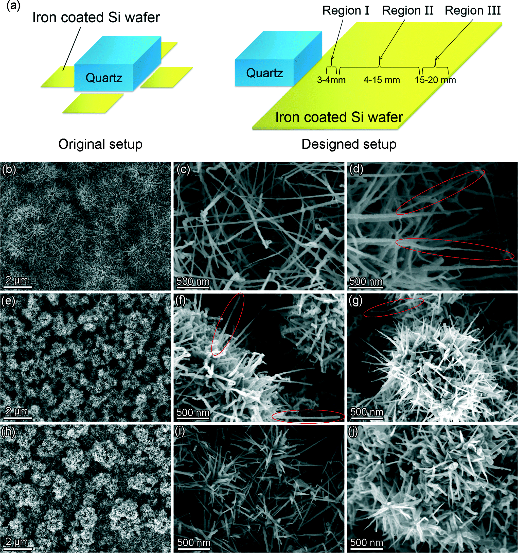 | ||
| Fig. 6 Morphology of the SiC nanostructures depending on the distance of the areas in Si wafer to quartz, (a) schematic geometry of the sample for experiment, comparing with the original setup, (b) low magnification SEM image of the SiC nanostructures from Region I, (c) and (d) magnified SEM images of the SiC nanostructures from Region I, (e) low magnification SEM image of the SiC nanostructures from Region II, (f) and (g) magnified SEM images of the SiC nanostructures from Region II, (h) low magnification SEM image of the SiC nanostructures from Region III, (i) and (j) magnified SEM images of the SiC nanostructures from Region III. | ||
4. Conclusions
In conclusion, catalyst plays a key role in controlling the growth and morphology of 1D SiC nanostructures. The catalysts of Fe5Si3 and Fe3Si are found to favor the growth of SiC nanowires and nanoneedles, respectively. The growth of 1D SiC nanostructures follows the VSS mechanism and special crystallographic relation between the SiC nanowire and the Fe5Si3 catalyst was observed. The morphology of the SiC nanostructures, especially the lengths and the diameters, was determined by the composition variation and shape transformation of the catalyst particles, which was highly dependent on the Si concentrations. These findings open the door to controllable synthesis of 1D SiC nanostructures.Notes and references
- Y. Xia, P. Yang, Y. Sun, Y. Wu, B. Mayers, B. Gates, Y. Yin, F. Kim and H. Yan, Adv. Mater., 2003, 15, 353–389 CrossRef CAS PubMed.
- P. Yang, R. Yan and M. Fardy, Nano Lett., 2010, 10, 1529–1536 CrossRef CAS PubMed.
- Y. Wang, V. Schmidt, S. Senz and U. Gösele, Nat. Nanotechnol., 2006, 1, 186–189 CrossRef CAS PubMed.
- Y. Hao, G. Meng, Z. L. Wang, C. Ye and L. Zhang, Nano Lett., 2006, 6, 1650–1655 CrossRef CAS PubMed.
- X. Weng, R. A. Burke and J. M. Redwing, Nanotechnology, 2009, 20, 085610 CrossRef PubMed.
- Y.-C. Chou, C.-Y. Wen, M. C. Reuter, D. Su, E. A. Stach and F. M. Ross, ACS Nano, 2012, 6, 6407–6415 CrossRef CAS PubMed.
- L. Zhang, X. Fang and C. Ye, Controlled Growth of Nanomaterials, World Scientific, Singapore, 2007, pp. 13–14 Search PubMed.
- R. S. Wagner and W. C. Ellis, Appl. Phys. Lett., 1964, 4, 89–90 CrossRef CAS PubMed.
- A. I. Persson, M. W. Larsson, S. Stenström, B. J. Ohlsson, L. Samuelson and L. R. Wallenberg, Nat. Mater., 2004, 3, 677–681 CrossRef CAS PubMed.
- C.-Y. Wang, L.-H. Chan, D.-Q. Xiao, T.-C. Lin and H. C. Shih, J. Vac. Sci. Technol., B, 2006, 24, 613–617 CAS.
- F. M. Ross, Rep. Prog. Phys., 2010, 73, 114501 CrossRef.
- S. Hofmann, R. Sharma, C. T. Wirth, F. Cervantes-Sodi, C. Ducati, T. Kasama, R. E. Dunin-Borkowski, J. Drucker, P. Bennett and J. Robertson, Nat. Mater., 2008, 7, 372–375 CrossRef CAS PubMed.
- K. Kang, D. A. Kim, H.-S. Lee, C.-J. Kim, J.-E. Yang and M.-H. Jo, Adv. Mater., 2008, 20, 4684–4690 CrossRef CAS PubMed.
- L. C. Campos, M. Tonezzer, A. S. Ferlauto, V. Grillo, R. Magalhães-Paniago, S. Oliveira, L. O. Ladeira and R. G. Lacerda, Adv. Mater., 2008, 20, 1499–1504 CrossRef CAS PubMed.
- N. Han, A. T. Hui, F. Wang, J. J. Hou, F. Xiu, T. Hung and J. C. Ho, Appl. Phys. Lett., 2011, 99, 083114 CrossRef PubMed.
- K. Hillerich, M. E. Messing, L. Reine Wallenberg, K. Deppert and K. A. Dick, J. Cryst. Growth, 2011, 315, 134–137 CrossRef CAS PubMed.
- S. A. Dayeh, E. T. Yu and D. Wang, Nano Lett., 2007, 7, 2486–2490 CrossRef CAS PubMed.
- M. Jeppsson, K. A. Dick, J. B. Wagner, P. Caroff, K. Deppert, L. Samuelson and L.-E. Wernersson, J. Cryst. Growth, 2008, 310, 4115–4121 CrossRef CAS PubMed.
- C. Chèze, L. Geelhaar, A. Trampert, O. Brandt and H. Riechert, Nano Lett., 2010, 10, 3426–3431 CrossRef PubMed.
- S. G. Sundaresan, A. V. Davydov, M. D. Vaudin, I. Levin, J. E. Maslar, Y.-L. Tian and M. V. Rao, Chem. Mater., 2007, 19, 5531–5537 CrossRef CAS.
- G.-Y. Li, X.-D. Li, Z.-D. Chen, J. Wang, H. Wang and R.-C. Che, J. Phys. Chem. C, 2009, 113, 17655–17660 CAS.
- Z. Liu, V. Srot and J. C. Yang, Appl. Phys. Lett., 2010, 96, 253111 CrossRef PubMed.
- R. Wu, K. Zhou, J. Wei, Y. Huang, F. Su, J. Chen and L. Wang, J. Phys. Chem. C, 2012, 116, 12940–12945 CAS.
- H. Yu, J. Han, J. Zhu and W. Cao, CrystEngComm, 2013, 15, 4655–4659 RSC.
- P. Lu, Q. Huang, A. Mukherjee and Y.-L. Hsieh, J. Mater. Chem., 2011, 21, 1005–1012 RSC.
- H. Wang, Z. Xie, W. Yang, J. Fang and L. An, Cryst. Growth Des., 2008, 8, 3893–3896 CAS.
- R. Wu, B. Li, M. Gao, J. Chen, Q. Zhu and Y. Pan, Nanotechnology, 2008, 19, 335602 CrossRef PubMed.
- M. Negri, S. C. Dhanabalan, G. Attolini, P. Lagonegro, M. Campanini, M. Bosi, F. Fabbri and G. Salviati, CrystEngComm, 2015, 17, 1258–1263 RSC.
- H. Morkoç, S. Strite, G. B. Gao, M. E. Lin, B. Sverdlov and M. Burns, J. Appl. Phys., 1994, 76, 1363–1398 CrossRef PubMed.
- J. B. Casady and R. W. Johnson, Solid-State Electron., 1996, 39, 1409–1422 CrossRef.
- Z. Li, J. Zhang, A. Meng and J. Guo, J. Phys. Chem. B, 2006, 110, 22382–22386 CrossRef CAS PubMed.
- J. C. Li, C. S. Lee and S. T. Lee, Chem. Phys. Lett., 2002, 355, 147–150 CrossRef CAS.
- G. Shen, Y. Bando, C. Ye, B. Liu and D. Golberg, Nanotechnology, 2006, 17, 3468 CrossRef CAS PubMed.
- Y. Zhang, X. Han, K. Zheng, Z. Zhang, X. Zhang, J. Fu, Y. Ji, Y. Hao, X. Guo and Z. L. Wang, Adv. Funct. Mater., 2007, 17, 3435–3440 CrossRef CAS PubMed.
- D.-H. Wang, D. Xu, Q. Wang, Y.-J. Hao, G.-Q. Jin, X.-Y. Guo and K. N. Tu, Nanotechnology, 2008, 19, 215602 CrossRef PubMed.
- H. Zhuang, C. Wang, N. Huang and X. Jiang, Electrochem. Commun., 2014, 41, 5–7 CrossRef CAS PubMed.
- H. Zhuang, L. Zhang, T. Staedler and X. Jiang, Appl. Phys. Lett., 2012, 100, 193102 CrossRef PubMed.
- G. Z. Yang, H. Cui, Y. Sun, L. Gong, J. Chen, D. Jiang and C. X. Wang, J. Phys. Chem. C, 2009, 113, 15969–15973 CAS.
- H. J. Li, Z. J. Li, A. L. Meng, K. Z. Li, X. N. Zhang and Y. P. Xu, J. Alloys Compd., 2003, 352, 279–282 CrossRef CAS.
- J.-S. Lee, Y.-K. Byeun, S.-H. Lee and S.-C. Choi, J. Alloys Compd., 2008, 456, 257–263 CrossRef CAS PubMed.
- J. Lacaze and B. Sundman, Metall. Trans. A, 1991, 22, 2211–2223 CrossRef.
- R. Ma, J. Huang, X. Xiong, M. Fan, W. Yan and Q. Xie, Phys. Status Solidi C, 2013, 10, 1750–1752 CrossRef CAS PubMed.
- Y. Zhang and D. G. Ivey, J. Mater. Sci., 1998, 33, 3131–3135 CrossRef CAS.
- N. R. Baldwin and D. G. Ivey, J. Phase Equilib., 1995, 16, 300–307 CrossRef CAS.
- S. Kadečková and K. Voleník, Czech. J. Phys. B, 1967, 17, 649–650 CrossRef.
Footnote |
| † Electronic supplementary information (ESI) available: Supplementary TEM images of the SiC nanowire and nanoneedle, EDS spectra of the catalysts and AFM images showing the dewetting effect after the H2 plasma etching. See DOI: 10.1039/c5ce00865d |
| This journal is © The Royal Society of Chemistry 2015 |