
 Open Access Article
 This Open Access Article is licensed under a
 Creative Commons Attribution 3.0 Unported Licence
Compositional tunability in solid solution PbSxSe1−x thin films chemically deposited on GaAs(100)
Tsofnat
Safrani
ab and
Yuval
Golan
*ab
aDepartment of Materials Engineering, Ben-Gurion University of the Negev, Beer-Sheva 84105, Israel
bIlse Katz Institute for Nanoscale Science and Technology, Ben-Gurion University of the Negev, Beer-Sheva 84105, Israel. E-mail: ygolan@bgu.ac.il; Fax: +972 8 6472944; Tel: +972 8 6461474
First published on 25th February 2015
Abstract
Compositional tuning of ternary solid solution semiconducting thin films can provide control over the physical properties of the films, and subsequently improve their technological performance. In this work, PbSxSe1−x solid solution thin films were chemically deposited on GaAs(100) substrates. Graded solid solutions as well as single-phase solid solutions with tunable compositions were obtained. Lattice parameters were extracted from X-ray diffraction and film compositions were calculated based on Vegard's law. It was concluded that PbSxSe1−x solid solution films can be chemically deposited in the entire range of compositions; however, each composition requires optimization of its own deposition conditions.
1. Introduction
Lead chalcogenides such as lead sulfide (PbS) and lead selenide (PbSe) are technologically important semiconducting materials with IR sensitivity, suitable for use as infrared radiation detectors, infrared emitters, solar control coatings and other optical applications.1–4 There are several techniques for fabricating high quality semiconducting thin films, and chemical bath deposition (CBD) is one of the simplest and most cost effective methods.5,6 Mixed compositions are of great interest mainly because they allow tuning of the semiconductor properties. Tuning of the material lattice parameter can allow control over the lattice mismatch in chemical epitaxy,7 and more importantly, can allow control over its physical properties such as tuning of the spectral sensitivity range for photoconductive detectors. This is probably the main application that accelerated the study of chemically deposited ternary and quaternary semiconductors. When chemically depositing mixed compositions of metal chalcogenides, the deposition should proceed according to the solubility product (ksp) of the two different chalcogenides; the first to precipitate is the one with the lower ksp, and only when the concentration of its free metal ions is low enough, the other chalcogenide will precipitate.5There are various possibilities for co-precipitation of two metal sulfides. For example, in the case at which both sulfides have a similar ksp (such as in CdS and PbS) mixed phase particles or single phase particles may directly precipitate, depending on the miscibility of the two phases. However, if the two sulfides have significantly different ksp values, core–shell structures may be formed.5 Several studies focused on compositions with two different metal cations such as Cd,Zn, Cd,Hg and Pb,Hg sulfides or selenides.8–16 Rabinovich et al., for example, reported on (Pb,Cd)S solid solutions.17 Mixed anion chalcogenide compounds, such as Cd(S,Se), Zn(S,Se) and Pb(S,Se), were deposited mainly in order to improve window layers for photovoltaic cells.18–26 Kigel et al. described a novel synthetic method for the formation of PbSe/PbSexS1−x core-alloyed shell nanocrystals by utilizing a single-injection of the core and shell constituents, simultaneously.27 They suggested that the faster reactivity of selenide to the lead precursor, directs rapid nucleation of the PbSe core, while the sulfide reacts at a later stage, forming the PbSexS1−x shell. Another study by Ma et al. reported on solar cells based on highly confined nanocrystals of the ternary compound PbSxSe1−x.28 The nanocrystals were obtained using a one-pot, hot injection reaction. It was reported that S and Se anions are uniformly distributed in the alloy nanoparticles, and that photovoltaic devices fabricated using these ternary nanoparticles were more efficient than either pure PbS or pure PbSe based nanocrystal devices since ternary PbSxSe1−x can simultaneously optimize both carrier transport (which is better in PbSe) and voltage (which is better in PbS).28
Very few publications reported on CBD of PbSxSe1−x thin films. Sarma et al. reported in the late 1980s on uniform and single phase PbSxSe1−x (0 < x < 1) films that were chemically deposited at 30 °C on glass and Si(111) substrates using Pb(NO3)2, CS(NH2)2 and Na2SeSO3 with excess of NaOH.29 These authors reported control over the final solid solution parameters that were calculated from the XRD results using Vegard's law.30 However, the morphology of the films was not investigated and no optimization was carried out for obtaining a large range of solid solution compositions. More recently, Katisheva et al. reported on chemically deposited PbSySe1−y films on ‘pyroceram’ platelets.31,32 Two different compositions were reported with different reagent concentrations; one was S-rich PbS0.85Se0.15 and the second was Se-rich PbS0.07Se0.93. No studies have reported chemically deposited PbSxSe1−x solid solutions on GaAs substrate, and there is still a lack of information on the morphology and structure of the films deposited on glass or silicon substrates, as well as on the different conditions required for obtaining PbSxSe1−x solid solutions in a complete range of compositions.
PbS and PbSe possess the rock-salt crystal structure with unit cell parameters a0 = 5.934 Å (JCPDS file #5-592) and a0 = 6.128 Å (JCPDS file #6-354), respectively.33 The physical and chemical properties of PbS and PbSe have much in common: they are isomorphous, have the same type of chemical bonding, can be prepared by similar methods, and they can be doped in a similar manner.34 Additionally, their anionic radii are within 15% of each other, the lattice mismatch parameter is only 3%, and the anions are isovalent.28 All these properties suggest that PbS and PbSe are likely to form an ideal substitutional alloy in the entire range of compositions. However, as described above, thermodynamic considerations in CBD can constitute an obstacle in achieving that goal. Templeman et al. recently reported on the effect of substrate surface pre-treatments and the importance of the order of reagent addition;35 PbS films are usually deposited with Pb precursor added first36 while PbSe films are normally deposited with Pb precursor added last.37 This can now present a challenge while attempting to simultaneously deposit both chalcogenide species from the same solution.
In this work, we have optimized the deposition conditions required for fabricating homogenous, continuous and adherent PbSxSe1−x solid solution films with tunable lattice parameters and compositions in the entire range of compositions. Deposition parameters such as temperature, reagent concentration, pH and deposition time were optimized and eventually high quality, homogeneous, continuous and adherent films with tunable compositions and lattice parameters were obtained.
2. Experimental section
2.1 Materials and chemicals
Lead nitrate Pb(NO3)2 (Aldrich, analytical 99.99+%) or lead acetate trihydrate Pb(CH3COOH)2·3H2O (Aldrich, analytical 99+%) were the precursors used for lead cations. Thiourea (TU) CS(NH2)2 (Aldrich, ACS ≥99.0%) was the precursor used for sulfide anions and sodium selenosulfate Na2SeSO3 was the precursor used for selenide anions. A 0.2 M stock solution of sodium selenosulfate was prepared by mixing sodium sulfite (0.5 M) (Na2SO3, Aldrich, analytical 99.95%) with an excess of selenium powder (Aldrich, 100 mesh, analytical 95+%) in distilled water and stirred at 80 °C for 1 h. The Na2SeSO3 solution was filtered in order to remove unreacted selenium powder. Sodium hydroxide NaOH (Gadot, AR) or potassium hydroxide KOH were used as sources for hydroxide anion complexants and pH stabilizers. Rectangular (1 × 2 cm2) substrates were cleaved from 3" GaAs(100) wafers (Wafer Technology LTD). Distilled water was obtained from a Millipore Direct Q3 water purification system.2.2 Chemical bath deposition (CBD)
The deposition procedure was adapted from the experimental protocol reported by Sarma et al. for deposition on glass substrate,29 and modified based on the deposition procedures reported for the growth of PbSe and PbS films on GaAs.24,36,37 For the growth of PbSxSe1−x on GaAs the final composition of the deposition solution was adjusted to 146–300 mM NaOH, 9 mM Pb(NO3)2, and 51 mM for the total anion precursors – CS(NH2)2 and Na2SeSO3. Films were deposited from solutions with variable values of RSe, which is defined as the percent ratio of sodium selenosulfate to the total anion precursor content (eqn (1)). | (1) |
Prior to deposition, the solution was prepared in a Pyrex beaker and purged with pure N2 for 60 min to minimize levels of dissolved oxygen and carbon dioxide, and placed in the dark in a thermostatic bath to reach thermal equilibrium. As the desired deposition temperature was reached, the last reactant was added. The growth of PbSxSe1−x films was carried out under various deposition temperatures and at different reagent concentrations with different order of reagent addition. Films were deposited on the bottom face of the substrates to prevent from large particles to adhere to the growing film. Therefore, the substrates were placed epi-side down in the solution, mounted on a custom-designed Teflon stage at an angle of ~70° with respect to the stage surface. After deposition, the samples were cleaned with ethanol and dried with a stream of N2 gas.
2.3 Characterization methods
3. Results and discussion
In this work, we have aimed to identify the CBD growth conditions for growing PbSxSe1−x solid solution thin films on GaAs(100) substrate in the entire range of compositions. The influence of deposition time, temperature, pH, reagent concentrations and order of reagent addition on the composition, structure and morphology of the films was investigated using XRD and HRSEM.3.1 Effect of anion ratio
The composition, structure and morphology of the films were investigated as a function of the anion ratio in the deposition solution. Fig. 1 shows SEM micrographs of films deposited at 30 °C for 120 min with 146 mM NaOH and variable values of RSe. These deposition conditions were optimised for growth of PbS films on GaAs substrate;24,36 thus, a typical morphology indicative of a <110> texture was obtained for the pure-PbS film (Fig. 1a).7 This texture was eliminated upon increasing RSe as can be seen in Fig. 1. This is also seen in the I220/I200 intensity ratio plotted vs. RSe (Fig. 2); the preferred texture disappears upon increasing RSe to ≥2%. At RSe ≥ 18% the large, faceted crystals are replaced with very small nanoparticles that, according to XRD analysis, are diffraction amorphous and crystallize only after annealing at 200 °C for 120 min (not shown). | ||
| Fig. 1 HRSEM images of films deposited at 30 °C for 120 min with 146 mM NaOH and different RSe values as indicated. | ||
 | ||
| Fig. 2 XRD (220)/(200) peak intensity ratio for films deposited at 30° C for 120 min, from solutions with different RSe values. Note the different scales for R values along the x-axis. | ||
PbSe films are typically grown from solutions with higher pH (>13) and with lead acetate precursor added last.37 Thus, growth of PbSe under conditions that are optimized for PbS (with pH > 12)36 resulted in non-typical morphology of small and rounded amorphous particles as in Fig. 1j. It should be noted however, that an ultrathin amorphous PbSe has been previously reported to form under typical deposition conditions as an interfacial layer between the crystalline PbSe film and the GaAs substrate.37
Fig. 3 shows (200) XRD peaks of films deposited at 30 °C with 146 mM NaOH and with different RSe values. The vertical dashed lines indicate the (200) peak positions according to the JCPDS powder diffraction files: #5-592 for PbS (turquoise) and #6-354 for PbSe (orange).
 | ||
| Fig. 3 XRD patterns showing (200) peak of (a) film deposited at 30 °C for 120 min from solution with RSe = 10% and 146 mM NaOH. The turquoise, red and green curves represent deconvolution of the as-measured diffractogram (black curve). Inset shows a corresponding HRSEM image showing mixed microstructure. (b) Films deposited from solution with RSe = 18% and 27%. The vertical dashed lines indicate the theoretical powder (200) peak positions according to the JCPDS powder diffraction files: #5-592 for PbS (turquoise) and #6-354 for PbSe (orange). | ||
For simplicity, we choose to show only (200) peaks since different films grow with different morphologies, orientations and peak intensity ratios, while (200) peak is in most cases the dominant one. As can be seen in Fig. 3a and in the HRSEM inset, coexistence of three phases was obtained in the film with RSe = 10%. An initial Se-rich layer with an average composition of PbS0.34Se0.66 (solid solution ‘a’), an additional overgrown S-rich layer with an average composition of PbS0.84Se0.16 (solid solution ‘b’) and particles comprising pure PbS deposited on top of the film. These are average compositions as the peaks are relatively wide and probably represent a range of solid solutions (according to their FWHM compared with that of a single phase peak) with graded compositions. The average compositions were calculated using Vegard's law (eqn (2))
| aPbSxSe1−x = xaPbS + (1 − x)aPbSe | (2) |
The Se-rich layer tends to grow first due to the lower ksp of PbSe (~4 × 10−37 at 25 °C) compared with that of PbS (~3 × 10⁻²⁸ at 25 °C). As the sodium-selenosulfate concentration in solution decreases, a S-rich film begins to form. This S-rich phase was also reported by Katysheva et al.31 Finally, when the Se ion source depletes, pure PbS particles are formed. According to Fig. 3b, it appears that the low ksp of PbSe allows to obtain highly Se-rich films despite the relatively low molar concentration of sodium selenosulfate in the deposition solution since PbS0.11Se0.89 and PbS0.03Se0.97 (corresponding to solid solutions ‘d’ and ‘e’ in Fig. 3b) were obtained with relatively low RSe values of 18% and 27%, respectively.
3.2 Compositional tunability
In order to eliminate phase separation and overcome the effect of the different ksp of PbS and PbSe, the effect of temperature and pH was investigated. | ||
| Fig. 4 XRD patterns showing (200) peaks for films deposited at 30 °C for 120 min and 50 °C for 30 min from solution with RSe = 10% and 146 mM NaOH. In the latter case, single phase solid solution (PbS0.55Se0.45) was obtained. | ||
The solubility product is a temperature and pH dependent parameter. It has an Arrhenius dependency on temperature as shown in eqn (3).5
 | (3) |
However, an attempt to use higher deposition tempterature and shorter deposition time for obtaining solid solution films in a wide range of compositions resulted in randomly distributed solid solution particles (Fig. 5a and b; the case of Se-rich films) or graded solid solution films (Fig. 5a and c; the case of S-rich films). Apparently, the change in the S to Se precursor ratio in solution had a tremendous effect on film morphology on one hand (in Se-rich films), and film composition on the other (in S-rich films). This is not surprising considering the previous discussion on the effect of anions ratio given their different reactivities and the different deposition conditions suitable for fabricating PbS and PbSe films.
 | ||
| Fig. 5 (a) XRD patterns showing gradual shift of the (200) peak with R for films deposited at 50 °C for 15 min. (b) HRSEM plan-view showing randomly distributed particles (of Se-rich solid solution with R = 23%). (c) HRSEM plan-view showing continuous film (of S-rich graded solid solution with R = 5%). | ||
 | ||
| Fig. 6 XRD patterns showing (200) peaks for a film deposited at 30 °C for 120 min with RSe = 10% and 300 mM NaOH. In this case, Se-rich solid solution (PbS0.342Se0.66) was almost entirely eliminated and the majority of the solid solution was S-rich (PbS0.82Se0.18). | ||
Additionally, the Pb precursor is added first which is optimal for PbS deposition.36 Thus, S-rich solid solution film was obtained (the small amount of Se-rich phase is due to the lower ksp of PbSe and the relatively low deposition temperature of 30 °C). Again, considering the previous discussion on temperature and time effect, lower deposition temperature of 20 °C and shorter deposition time of 60 min resulted in the isolation of the Se-rich solid solution film ‘a’ (PbS0.39Se0.61), as can be seen in Fig. 7.
 | ||
| Fig. 7 XRD pattern showing the (200) peak for a film deposited at 20 °C for 60 min with RSe = 10% and 300 mM NaOH. In this case, a Se-rich solid solution (PbS0.392Se0.61) was isolated. | ||
At this point, several single phase solid solutions were obtained, each with its specific deposition conditions. However, in order to obtain different solid solutions in the entire range of compositions, further modification of the Se![[thin space (1/6-em)]](https://www.rsc.org/images/entities/char_2009.gif) :S precursor ratio in solution is needed, and that requires additional optimization. For example, Fig. 8a and b shows films deposited from the same deposition conditions previously mentioned (of relatively high pH with 300 mM NaOH) but with RSe = 50%. The change of the S/Se precursor ratio resulted in randomly distributed particles rather than a film. This is probably due to the PbS-optimized conditions while the concentration of the more reactive Se precursor in solution is relatively high.
:S precursor ratio in solution is needed, and that requires additional optimization. For example, Fig. 8a and b shows films deposited from the same deposition conditions previously mentioned (of relatively high pH with 300 mM NaOH) but with RSe = 50%. The change of the S/Se precursor ratio resulted in randomly distributed particles rather than a film. This is probably due to the PbS-optimized conditions while the concentration of the more reactive Se precursor in solution is relatively high.
 | ||
| Fig. 8 (a) and (b) are plan-view and cross-section HRSEM images of a film deposited at 30 °C with 300 mM NaOH and RSe = 50%. (c) and (d) are plan-view and cross-section HRSEM images of a film deposited under the same conditions but with Pb precursor added last. (e) XRD (200) peak obtained from the film shown in c, d. | ||
Thus, an attempt to grow films under conditions optimized for PbSe (for Se-rich films) was carried out, namely films were deposited under the same deposition conditions but with the Pb-precursor added last (reversed order of reagent addition35). The result obtained was strikingly different. As can be seen in Fig. 8c and d, continuous and adherent film of single phase Se-rich solid solution with a composition of PbS0.23Se0.77 was obtained (based on the XRD peak position in Fig. 8e). Under these conditions several additional Se-rich films with different compositions were obtained. Fig. 9 shows X-ray diffractograms of several representative solid solution films obtained in a wide range of compositions between PbSe and PbS with the corresponding lattice parameter. Each solid solution was obtained following optimization of its specific deposition conditions (Table 1 summarize their properties). Highly S-rich solid solutions were deposited under PbS-optimized conditions with relatively higher temperature or relatively high pH and with the chalcogenide precursor added last. Highly Se-rich solid solutions were deposited under PbSe-optimized conditions with relatively high pH, lower deposition temperature and time and with Pb precursor added last. Relatively equally mixed compositions were obtained at higher deposition temperature and shorter deposition time. Note that PbS0.28Se0.72 solid solution might be better to grow with higher pH and with lead precursor added last in order to obtain continuous film.
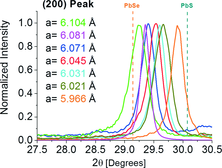 | ||
| Fig. 9 (200) XRD peak obtained for PbSxSe1−x films with different compositions. The vertical dashed lines indicate the theoretical powder (200) peak positions for PbS (JCPDS powder diffraction file # 5-592) (turquoise) and PbSe (JCPDS file # 6-354) (orange). | ||
| Cell parameter | R Se [%] | Composition | Morphology | Experimental conditions: temp./time/NaOH conc./last added precursor[°C]/[min]/mM |
|---|---|---|---|---|
| 6.104 | 70 | PbS0.11Se0.89 | ~250 μm poly-crystalline film | 20/60/300 lead |
| 6.081 | 50 | PbS0.23Se0.77 | ~400 μm poly-crystalline film | 30/120/300 lead |
| 6.071 | 50 | PbS0.28Se0.72 | Distributed particles | 50/30/146 TU |
| 6.045 | 10 | PbS0.42Se0.58 | ~250 μm poly-crystalline film | 50/15/146 TU |
| 6.031 | 8 | PbS0.50Se0.50 | ~400 μm poly-crystalline film | 50/15/146 TU |
| 6.021 | 10 | PbS0.55Se0.45 | ~600 μm poly-crystalline film | 50/30/146 TU |
| 5.966 | 10 | PbS0.84Se0.16 | ~500 μm poly-crystalline film | 40/90/300 TU |
4. Conclusions
We have shown that PbSxSe1−x solid solution films can be obtained in a complete range of compositions using chemical bath deposition on GaAs(100) substrates. It was found that the composition and morphology of the films are highly affected by temperature, concentrations (most notably, pH) and the order of reagent addition. It was concluded that each range of composition (Se:S ratio in the solid solution) requires optimization of specific deposition conditions and there is no single recipe for fabricating different PbSxSe1−x solid solution films in the entire composition range. Fabrication of solid solution films with tunable compositions and hence tunable lattice parameters can allow control over film-substrate lattice mismatch in chemical epitaxy,7 as well as tuning of the band gap energy of the semiconducting material, providing control over physical properties such as optical absorption and emission.
Acknowledgements
We thank Dr. Dmitry Mogilyansky for expert assistance in XRD. This work was partially funded by the Israel Science Foundation under Grant #156/14.Notes and references
- P. K. Nair, M. T. S. Nair, A. Fernandez and M. Ocampo, J. Phys. D: Appl. Phys., 1989, 22, 829–836 CrossRef CAS.
- P. Capper and C. T. Eliot, Infrared Detectors and Emitters: Materials and Devices, Kluver Academic Publishers, 2001 Search PubMed.
- P. K. Nair and M. T. S. Nair, J. Phys. D: Appl. Phys., 1990, 23, 150–155 CrossRef CAS.
- M. K. Jana, B. Murali, S. B. Krupanidhi, K. Biswas and C. N. R. Rao, J. Mater. Chem. C, 2014, 2, 6283–6289 RSC.
- G. Hodes, Chemical Solution Deposition of Semiconductor Films, M. Dekker, New-York, 2003 Search PubMed.
- D. L. Smith, Thin Film Deposition, Principles and Practice, McGraw-Hill, 1995, ch. 6, p. 229 Search PubMed.
- A. Osherov and Y. Golan, MRS Bull., 2010, 35, 790–796 CrossRef CAS.
- K. L. Chopra, R. C. Kainthla, D. K. Pandya and A. P. Thakoor, Physics of Thin Films, 12th edn, 1982 Search PubMed.
- A. Upcher, V. Ezersky, A. Berman and Y. Golan, Cryst. Growth Des., 2013, 13, 2149–2160 CAS.
- R. K. Joshi, A. Kanjilal and H. K. Sehgal, Nanotechnology, 2003, 14, 809–812 CrossRef CAS.
- Y. F. Nicolau, M. Dupuy and M. Brunel, J. Electrochem. Soc., 1990, 137, 2915–2924 CrossRef CAS PubMed.
- L. P. Deshmukh, K. M. Garadkar and D. S. Sutrave, Mater. Chem. Phys., 1998, 55, 30–35 CrossRef CAS.
- S. T. Mane, S. S. Kamble, S. A. Lendave and L. P. Deshmukh, Mater. Lett., 2012, 67, 373–375 CrossRef CAS PubMed.
- M. A. Barote, S. S. Kamble, L. P. Deshmukh and E. U. Masumdar, Ceram. Int., 2013, 39, 1463–1467 CrossRef CAS PubMed.
- S. C. Ray, M. K. Karanjai and D. Dasgupta, Thin Solid Films, 1998, 332, 117–122 CrossRef.
- M. K. Jana, P. Chithaiah, B. Murali, S. B. Krupanidhi, K. Biswas and C. N. R. Rao, J. Mater. Chem. C, 2013, 1, 6184–6187 RSC.
- E. Rabinovich, E. Wachtel and G. Hodes, Thin Solid Films, 2008, 517, 737–744 CrossRef CAS PubMed.
- A. I. Lebedev and I. A. Sluchinskaya, Ferroelectrics, 1994, 157, 275–280 CrossRef CAS.
- A. I. Lebedev and I. A. Sluchinskaya, J. Alloys Compd., 1994, 203, 51–54 CrossRef CAS.
- H. Zogg, C. Maissen, J. Masek, T. Hoshino, S. Blunier and A. N. Tiwari, Semicond. Sci. Technol., 1991, 6, C36–C41 CrossRef CAS.
- K. J. Linden, K. W. Nill and J. F. Butler, IEEE J. Quantum Electron., 1977, 13, 720–725 CrossRef.
- S. Kumar, Opt. Mater., 2004, 25, 25–32 CrossRef CAS.
- R. B. Schoolar, J. D. Jensen, G. M. Black, S. Foti and A. C. Bouley, Infrared Phys., 1980, 20, 271–275 CrossRef CAS.
- S. Kacimi, A. Zaoui, B. Abbar and B. Bouhafs, J. Alloys Compd., 2008, 462, 135–141 CrossRef CAS PubMed.
- R. Kumar, G. Jain, R. Saini and P. Agarwal, Chalcogenide Lett., 2010, 7, 233–240 CAS.
- J. Akhtar, M. Afzaal, M. Banski, A. Podhorodecki, M. Syperek, J. Misiewicz, U. Bangert, S. J. O. Hardman, D. M. Graham, W. R. Flavell, D. J. Binks, S. Gardonio and P. O'Brien, J. Am. Chem. Soc., 2011, 133, 5602–5609 CrossRef CAS PubMed.
- A. Kigel, M. Brumer, A. Sashchiuk, L. Amirav and E. Lifshitz, Mater. Sci. Eng., C, 2005, 25, 604–608 CrossRef PubMed.
- W. Ma, J. M. Luther, H. Zheng, Y. Wu and A. P. Alivisatos, Nano Lett., 2009, 9, 1699–1703 CrossRef CAS PubMed.
- Y. S. Sarma, N. K. Misra and H. N. Acharya, Indian J. Phys., 1989, 63A, 445–456 CAS.
- L. Vegard, Z. Med. Phys., 1921, 5, 17–26 CrossRef CAS.
- A. S. Katysheva, V. F. Markov, L. N. Maskaeva and A. V. Chukin, Chem. Chem. Technol., 2012, 55, 131 Search PubMed.
- A. S. Katysheva, V. F. Markov and L. N. Maskaeva, Russ. J. Inorg. Chem., 2013, 58, 833–838 CrossRef CAS.
- Y. Noda, S. Ohba, S. Sato and Y. Saito, Acta Crystallogr., Sect. B: Struct. Sci., 1983, 39B, 312–317 CrossRef.
- S. Kumar, Z. H. Khan, M. A. M. Khan and M. Husain, Curr. Appl. Phys., 2005, 5, 561–566 CrossRef PubMed.
- T. Templeman, M. Biton, T. Safrani, M. Shandalov, E. Yahel and Y. Golan, CrystEngComm, 2014, 16, 10553–10559 RSC.
- A. Osherov, V. Ezersky and Y. Golan, Eur. Phys. J.: Appl. Phys., 2006, 37, 39–47 CrossRef.
- M. Shandalov and Y. Golan, Eur. Phys. J.: Appl. Phys., 2003, 24, 13–20 CrossRef CAS.
- A. Osherov, V. Ezersky and Y. Golan, J. Cryst. Growth, 2007, 308, 334–339 CrossRef CAS PubMed.
| This journal is © The Royal Society of Chemistry 2015 |