
Decoration of CdS nanoparticles on 3D self-assembled ZnO nanorods: a single-step process with enhanced field emission behaviour
Sambhaji S.
Warule
*ab,
Nilima S.
Chaudhari
ae,
Raju T.
Shisode
ce,
Keith V.
Desa
b,
Bharat B.
Kale
*d and
Mahendra A.
More
*e
aCentre of Excellence in Solar Energy, Physical and Materials Chemistry Division, National Chemical Laboratory (CSIR-NCL), Pune 411008, India. E-mail: warulesam@gmail.com
bDepartment of Physics, Nowrosjee Wadia College, Pune 411001, India
cDepartment of Electronics, Nowrosjee Wadia College, Pune 411001, India
dCentre for Materials for Electronics Technology (C-MET), Department of Electronics and Information Technology (DeitY), Govt. of India, Panchawati, Off Pashan Road, Pune-411 008, India. E-mail: bbkale@cmet.gov.in
eCenter for Advanced Studies in Materials Science and Condensed Matter Physics, Department of Physics, Savitribai Phule Pune University, Pune-411 007, India. E-mail: mam@physics.unipune.ac.in
First published on 6th November 2014
Abstract
A well-defined CdS–ZnO heteroarchitecture has been synthesized via a facile single-step hydrothermal approach. The morphological and structural studies reveal the formation of 3D nano-architectures, in which self-assembled ZnO nanorods (diameter ~50 nm) are well decorated with single crystalline CdS nanoparticles (size ~10 nm). The CdS–ZnO heteroarchitecture exhibits a remarkable change in the optical absorption due to the surface modification of ZnO nanorods by CdS. Surprisingly, under identical reaction conditions, the global ZnS nanoparticles are selectively grown at the apex of ZnO nanorods on the Zn substrate. Furthermore, a plausible growth mechanism has been presented on the basis of experimental results. Interestingly, the CdS–ZnO heteroarchitecture shows enhanced field emission properties such as low turn-on field, high emission current density and better current stability in comparison to other ZnO-based nanostructures. The present CdS–ZnO heteroarchitecture could be extended to other potential applications, such as chemical sensors, photodetectors, optoelectronic devices, and photocatalysts.
Introduction
Rational design and fabrication of inorganic semiconductor nanostructures as building blocks for functional materials and devices is the key to tailor a desired set of properties for specific applications in electronics, optics, biomedicine, field emission and micro/nanosystems.1–3 Especially, functionalization of the surface of wide bandgap semiconductors via decoration of nanostructures of narrow bandgap semiconducting nanoparticles may lead to tunable optically driven devices as well as the ability to modulate charge transfer.4–8 Currently, intensive work is focused on fabrication of 1D semiconducting heterostructures (for example, branched 3D structure of 1D systems) offering unprecedented physico-chemical properties enabling new opportunities to enhance their functionality.9–12 Thus, rational designing of heterostructures with improved performance or new approaches of synthesis and/or processing of existing nanomaterials is highly desirable.Field emission (FE)-based electron sources have commercial applications in high-resolution electron microscopes, cathodoluminescent flat panel displays, X-ray sources and microwave tubes. With respect to FE applications, as per the Fowler–Nordheim (FN) equation, electron emitters made up of low work function materials possessing a high field-enhancement factor have application potential, since they exhibit enhanced FE current at relatively lower applied voltages.13–15 The recent attempts towards improvement in the FE characteristics are due to development of the field emitters based on rationally designed heteroarchitectures. Here the rational design implies an effective combination of the prime dependent parameters, the work function and the field enhancement factor (high aspect ratio) of the emitter. A rationally designed heteroarchitecture involves the use of nanostructures with high aspect ratio (as one counterpart) and ‘modulation’ of work function of the first counterpart by the other nanostructures. Such heteroarchitecture characterized by high-density protrusions localizes and enhances the electric field, thereby facilitating electrons to tunnel through the tips at very low applied voltages and produce stable emission from a larger area.16,17
ZnO and CdS are direct bandgap II–VI semiconductors, which have been extensively investigated as field emitters, field effect transistors, photodetectors, and electrodes for photovoltaic and photo-electrochemical cells.18–22 Although a large number of synthesis methods have been used to explore abundant morphologies of ZnO, research on well-defined ZnO heterostructures via the facile approach is insufficient to date. The CdS–ZnO heterostructure with tailored geometry is expected to exhibit enhanced field electron emission behaviour due to tuning of the properties of individual counterparts, high emission efficiency and high electron mobility.23 Recently, Rakshit et al. have reported synthesis of CdS-decorated ZnO nanorod heterostructures through a combination of hydrothermal and pulsed laser deposition techniques.4 In comparison to the two-step synthesis process, a single-step solution-based approach has several advantages, such as low reaction temperatures, low cost, large scalability, and relatively simple procedure. However, the bottom-up approach towards the fabrication of CdS–ZnO heterostructures for an excellent FE performance remains a challenge to date. Earlier, Chen and co-workers selectively modified ZnO multipods with a series of wide and narrow bandgap semiconductors (ZnS, ZnSe, Bi2S3, and Cu2S).7
In the present study, a simple one-step hydrothermal method is used to design 3D self-assembled CdS–ZnO heteroarchitectures. The morphological, structural, optical, and FE properties of the synthesized heteroarchitecture have been investigated. Interestingly, the CdS–ZnO heteroarchitecture emitter exhibits superior FE characteristics to the CeO2–ZnO heterostructure emitter.
Experimental
Synthesis
The precursors zinc nitrate hexahydrate [Zn(NO3)2·6H2O], potassium hydroxide [KOH], cadmium nitrate [Cd(NO3)2·6H2O], thiourea [(NH3)2CS] and polyvinylpyrrolidone (PVP) were of analytical grade and used without further purification. In a typical synthesis process, first, 1.48 g of Zn(NO3)2·6H2O and 2.24 g of KOH were dissolved in 25 mL of de-ionized water in two separate beakers. Then, Zn(NO3)2·6H2O solution was slowly dropped into KOH solution under constant stirring to avoid formation of Zn(OH)2 colloids. Then, appropriate amounts of Cd(NO3)2·6H2O, (NH3)2CS and PVP were mixed in 50 mL of de-ionized water in another beaker. After that, both the solutions were mixed together and transferred into a Teflon-lined reactor (capacity ~100 ml) along with pre-cleaned Zn foil as a substrate. The reactor was put into a stainless steel autoclave and heated at 110 °C for 4 h. After completion of the reaction, the autoclave was allowed to cool naturally. The as-obtained product was washed with de-ionized water and ethanol several times and finally dried at 60 °C in air. Similarly, the Zn substrate with the ‘deposit’ was removed from the reactor, washed with de-ionized water and ethanol, and finally dried in air.Characterization
The structural analysis of the as-synthesized CdS–ZnO heteroarchitecture was carried out using an X-ray diffractometer (XRD, D8 Advance, Bruker AXS), whereas for the surface morphological studies, field-emission scanning electron microscope (FESEM, Hitachi S-4800) was used. Furthermore, in-depth structural and morphological investigations were performed using a transmission electron microscope (TEM, Technai G2 20 Twin, FEI) operated in high-resolution (HR) mode. The optical properties were revealed from the absorption spectrum recorded using a UV-visible-NIR spectrophotometer (Perkin-Elmer λ-950). The photoluminescence (PL) spectrum was recorded at room temperature using a xenon lamp as an excitation source (PL spectrometer; Perkin-Elmer-LS-55). The details of sample preparation for FESEM and field emission studies are mentioned in our earlier report.24Field emission
The field emission current versus applied voltage (I–V) and emission current versus time (I–t) characteristics were measured in a planar ‘diode’ configuration in an all-metal vacuum chamber evacuated to a base pressure of ~1.0 × 10⁻⁸ mbar. In a typical ‘diode’ configuration, a semitransparent phosphor screen acts as the anode, whereas the CdS–ZnO heteroarchitecture (sprinkled onto a piece of UHV compatible conducting carbon tape pasted on a stainless steel stub) served as the cathode. The FE measurements were carried out at a constant cathode–anode separation of ~1 mm. The emission current was acquired by varying the applied dc voltage with a step of 40 V (0–40 kV, Spellman, U.S.). Special care was taken to avoid any leakage current by ensuring proper grounding. The details of vacuum processing and FE measurements are described in detail elsewhere.24Results and discussion
Fig. 1 depicts the XRD patterns of both the bare ZnO (red colored) and the CdS–ZnO heteroarchitecture (black colored). The as-synthesized CdS–ZnO heteroarchitecture exhibits a set of well-defined diffraction peaks identical to that of ZnO. The diffraction peaks are indexed to the hexagonal wurtzite phase of ZnO (a = 0.3249 nm and c = 0.5206 nm; JCPDS file no. 036-1451). A careful observation of the diffraction spectrum reveals the presence of some low intense peaks (with relatively higher FWHM), which are indexed to the cubic phase of CdS (JCPDS file no. 080-0019). The diffraction peaks corresponding to the (111), (220) and (311) planes of cubic CdS are marked by arrows (shown in the inset). The relatively higher FWHM of the diffraction peaks due to CdS is indicative of its nanometric dimensions. No diffraction peaks corresponding to other phases or impurities are observed. Thus the XRD results clearly reveal the formation of CdS–ZnO heteroarchitecture under the prevailing experimental conditions. | ||
| Fig. 1 XRD patterns of bare ZnO (red) and as-synthesized CdS–ZnO heteroarchitecture (black). | ||
The surface morphology of the as-synthesized CdS–ZnO heteroarchitecture and ZnO (without addition of CdS precursors in the reaction solution) is depicted in Fig. 2. It is apparent that in both cases, the morphology is characterized by an assembly of branched structures of ZnO nanorods of nearly uniform size (an average length and diameter of 400 and 50 nm, respectively). However, a careful observation of the high-magnification SEM images of the CdS–ZnO heteroarchitecture (Fig. 2b and c) indicates the presence of CdS nanoparticles (size <20 nm) uniformly decorated on the ZnO nanorods. It is worth mentioning here that under the optimized process variables, in a single-step hydrothermal approach formation of an interesting CdS–ZnO architecture has been achieved. The inset of Fig. 2c displays the schematic orientation relationship of ZnO branches with CdS nanoparticle decoration on the same architecture. The morphology of the product in the absence of CdS precursors, i.e. bare ZnO looks quite similar (self-assembled ZnO nanorod-like structure) under identical experimental conditions.
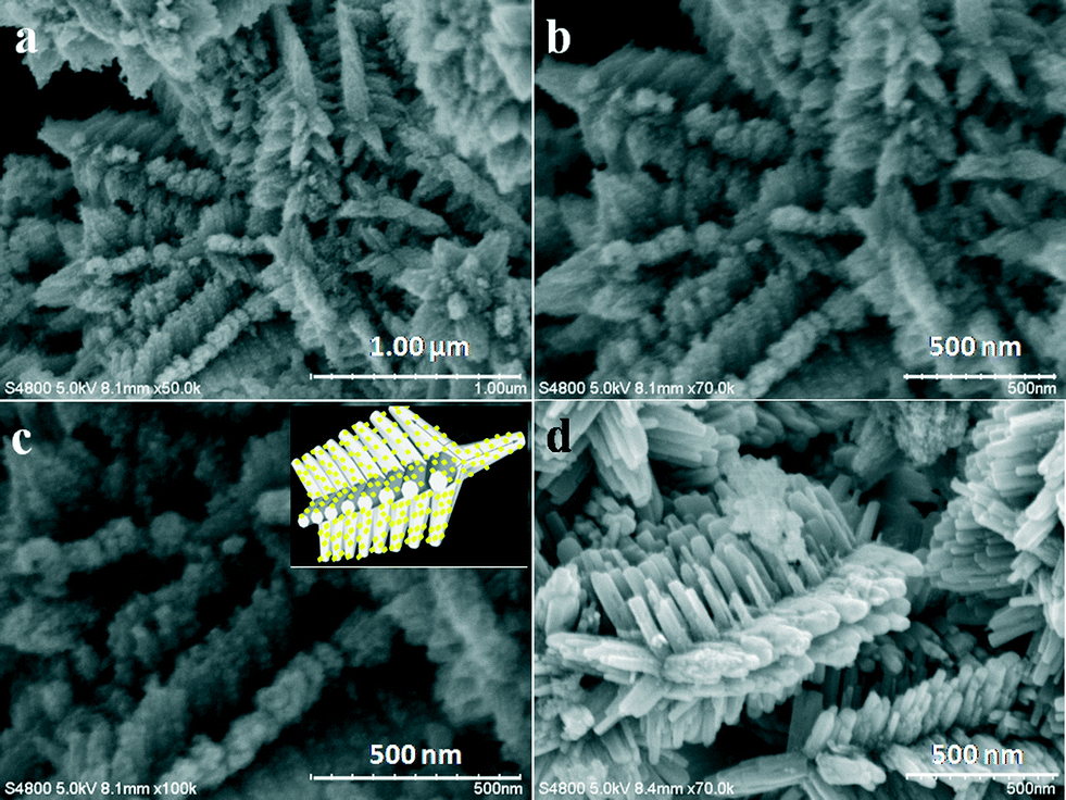 | ||
| Fig. 2 FESEM images of (a–c) as-synthesized CdS–ZnO heteroarchitecture and (d) bare ZnO. | ||
To understand the detailed structural characteristics of the synthesized product (CdS–ZnO heteroarchitecture), transmission electron microscopy (TEM) investigations were carried out. Fig. 3a shows a typical TEM image (low magnification) of the CdS–ZnO heteroarchitecture, supporting the SEM analysis results. The TEM image recorded at high magnification (Fig. 3b) reveals the presence of CdS nanoparticles (with bright contrast) uniformly decorating the ZnO nanorods. The average size of the CdS nanoparticles is observed to be ~10 nm. Fig. 3c and d present the high-resolution (HRTEM) images taken from an edge of a CdS–ZnO heteroarchitecture. The white circles marked in Fig. 3c indicate single crystalline CdS nanoparticles present on the surface of an individual ZnO nanorod. Fig. 3d reveals the crystalline nature of the ZnO nanorods. The digitally magnified view of the HRTEM image (Fig. 3e) gives interplanar distances of 2.75 and 5.3 Å, corresponding to the (110) and (001) planes of wurtzite ZnO, respectively. The single crystalline nature of the ZnO nanorod is further confirmed by the SAED (Fig. 3f). Furthermore, the interplanar spacing of 3.32 Å corresponds to the (111) plane of crystalline CdS. The appearance of rings along with spots in the SAED pattern of the CdS–ZnO heteroarchitecture (inset of Fig. 3b) may be due to orientation disorder between the ZnO nanorods and the CdS nanoparticles.
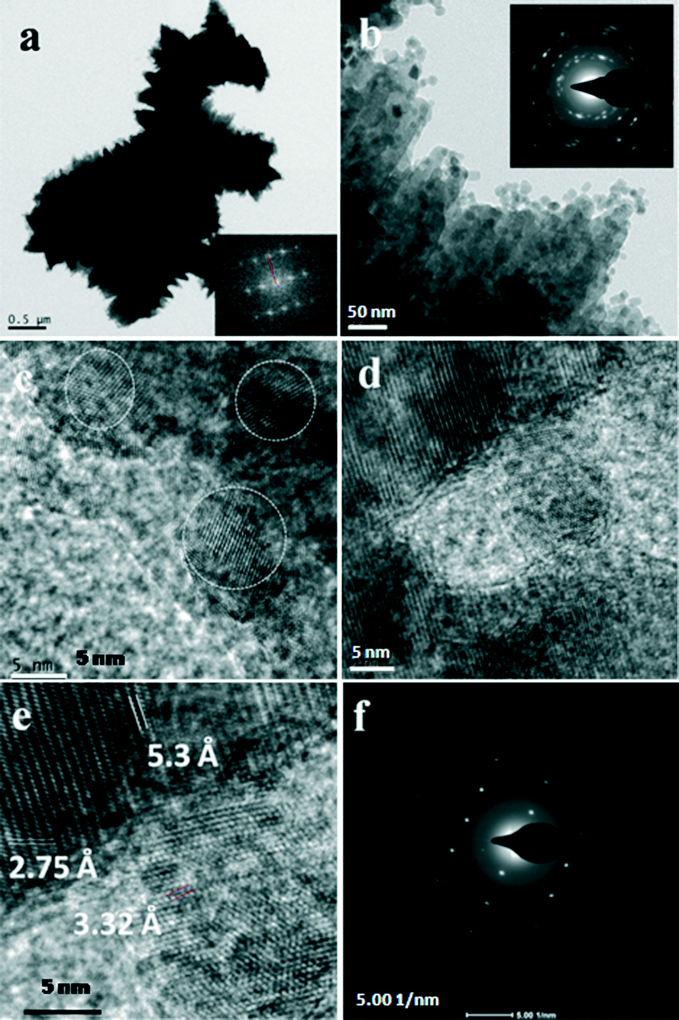 | ||
| Fig. 3 TEM images of the CdS–ZnO heteroarchitecture at (a) low and (b) high magnification with an inset depicting corresponding SAED pattern, (c–e) HRTEM images of a single ZnO nanorod with CdS nanoparticle, and (f) SAED pattern of ZnO nanorod. | ||
In order to reveal the influence of the substrate on the morphology of the CdS–ZnO heteroarchitecture, a piece of Zn foil was kept in the reaction bath during the synthesis process. Fig. 4a depicts the surface morphology of the deposit on Zn substrate, which is characterized by the hexagonal-shaped ZnO nanopencils with agglomerated CdS nanoparticles on their surface. The average diameter and length of ZnO pencils are found to be ~300 nm and 5 μm, respectively. At higher magnification (Fig. 4b), a sharp apex is observed along with the presence of a few CdS nanoparticles (average size ~10 nm).
 | ||
| Fig. 4 FESEM images on Zn foil under identical reaction conditions. (a, b) CdS–ZnO nanocomposite. | ||
Furthermore, interesting growth behaviour of CdS–ZnO nanostructures (as-synthesized powder and on Zn foil) was observed in the absence of the capping agent (PVP). In this case, an overall dense assembly of 3D flower-like surface morphology was observed (Fig. 5a). The magnified image of the ZnO flower (Fig. 5b) indicates that the nanorods/nanoplates of ZnO (average size ~ 60 nm and length ~1–2 μm) act as the backbone, which are covered with ~10 nm sized CdS nanoparticles. In comparison to the PVP-assisted growth, surface morphology is observed to be distinct, whereas interesting nanostructures were observed on Zn foil under identical conditions. In the low-magnification image (Fig. 5c), well-aligned ZnO nanorods (size ~150 nm) are mostly grown perpendicular to the surface of Zn foil. At high magnification (Fig. 5d), it is clearly seen that every tip of nanorods has been occupied by a global particle with the size around ~100 nm. It is interesting to see that these particles were selectively grown on the tips of the nanorods and were not found elsewhere. Such a type of unique ZnO-based heterostructure has been reported by Chen et al. for the ZnS–ZnO system.7
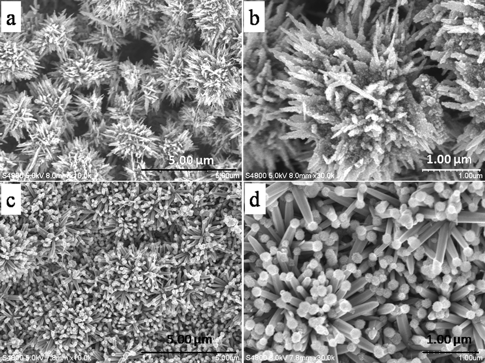 | ||
| Fig. 5 FESEM images of (a, b) CdS–ZnO heterostructures (powder sample) without PVP capping agents and (c, d) ZnS–ZnO heterostructure on Zn foil. | ||
For detailed structural investigations of these global nanoparticles, TEM analysis was carried out. Similar to the SEM morphology, a typical low-magnification TEM image (Fig. 6a) reveals the presence of global nanoparticles on the slightly tapered ZnO nanorods. The inset depicts a magnified view showing the presence of agglomerates of smaller-sized nanoparticles. The high-resolution TEM (HRTEM) image deliberately taken at the contact edge of ZnO nanorods and nanoparticles reveals the crystalline nature of the heteroarchitecture. From Fig. 6d, the spacing between adjacent lattice fringes is estimated to be ~2.78 Å, which is close to the d spacing of the (002) plane, representing the [001] direction, i.e. c-axis-oriented growth of the ZnO nanorods. Surprisingly, the nanoparticle shows lattice fringes with an interplanar spacing of 3.05 Å corresponding to the (111) plane of face-centered cubic ZnS. In support of the HRTEM results indicating formation of the ZnS phase, the EDS spectrum was taken on a globe of nanoparticles (Fig. 6c). The elemental analysis reveals the presence of Zn, S, and O only. Thus, the HRTEM and EDS analyses clearly indicate formation of ZnS–ZnO heteroarchitecture on ZnO foil under the prevailing experimental conditions. The selected area electron diffraction (SAED) pattern (inset of Fig. 6a) supports the formation of crystalline phases of both the ZnO nanorods and the ZnS nanoparticles.
 | ||
| Fig. 6 (a) TEM image of ZnS–ZnO heterostructures with inset depicting a magnified view of tip and SAED pattern, (b, d) HRTEM images, and (c) EDS spectrum recorded on the globe of nanoparticles (with the corresponding HRTEM image shown inset in Fig. c and d). | ||
The UV-visible absorption spectra of ZnO and CdS–ZnO heteroarchitecture are shown in Fig. 7. In the case of ZnO nanostructures an absorption edge at ~385 nm is observed with no apparent absorption in the visible region. In contrast, the CdS–ZnO heteroarchitecture shows noticeable absorption in the visible range (375–550 nm), which can be attributed to the presence of CdS nanoparticles on the ZnO nanorods.
 | ||
| Fig. 7 UV-Visible absorption spectra of (a) ZnO and (b) CdS–ZnO heteroarchitectures. | ||
In order to reveal the optical characteristics in detail photoluminescence (PL) spectra of the as-prepared ZnO and CdS–ZnO heteroarchitecture were recorded at room temperature (with an excitation wavelength of 325 nm). The PL spectrum of ZnO nanostructures (Fig. 8) shows three emission bands, including a near-UV emission around 380 nm, a strong blue emission at ~400–450 nm, and a broad green band at about 553 nm. In contrast to the ZnO nanostructures, the CdS–ZnO heteroarchitecture exhibits a broad luminescence centered at ~522 nm. The UV (near band edge) emission is due to the recombination of free excitons through an exciton–exciton collision process.25 The blue emission is likely linked to the radioactive defects at the interface of the components of ZnO or existence of interstitial zinc in ZnO lattices.26 It has been suggested that green band emission or deep-level emission (DLE) corresponds to the singly ionized oxygen vacancy in ZnO and results from the recombination of a photo-generated hole with the singly ionized charge state of this effect.27,28 A careful observation of the PL spectrum of the CdS–ZnO heteroarchitecture reveals the disappearance of the blue emission peak and the blue shift in the broad emission (~522 nm). This shift could be attributed to the change in oxygen vacancy centers by CdS. The broad emission peak centered at ~522 nm (which corresponds to the green–yellow emission) is attributed to the shallow defect transition of CdS nanoparticles. Recently, Huang and co-workers have demonstrated that the intensity of green luminescence from Cu-doped ZnO does not only depend on the annealing temperature but also on the annealing gas.29 The green luminescence is a result of charge transfer from the ZnO host to the Cu dopant and subsequent exciton recombination at the Cu dopant. In the present studies, this could be attributed to the decrease in the hydroxyl species on the ZnO surface due to the presence of the CdS nanoparticles in the heteroarchitecture. The maximum in the PL emission is “Stokes shifted” with respect to the absorption edge of ZnO and can be a favourable feature for many applications.30–32
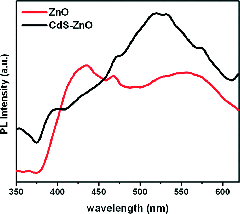 | ||
| Fig. 8 Photoluminescence spectrum of ZnO and CdS–ZnO heteroarchitectures. | ||
Growth mechanism
In order to reveal the growth mechanism of the CdS–ZnO heteroarchitecture, the growth process was monitored at various reaction intervals and temperatures, followed by analysis of the morphologies of the synthesized products. On the basis of the FESEM results, herein we present a plausible growth mechanism model of the heteroarchitecture schematically represented in Scheme 1. It is well known that controlled ZnO nanostructure formation took place via decomposition of Zn(OH)2 under hydrothermal conditions. Initially, ZnO nuclei are formed, which grow further into ZnO nanosheets through aggregation of the nanoparticles. Such ZnO nanosheets act as the backbone for the secondary growth. The formation of the self-assembled nanorods on the backbone (sheet) through the oriented growth mechanism leads to the formation of 3D ZnO nanostructures. In the case of CdS–ZnO heteroarchitecture, simultaneous growth of very tiny CdS nanoparticles occurs on the surface of ZnO nanorods. The growth rate of CdS nanoparticles is found to be smaller than that of ZnO, which is attributed to their solubility product constant [Ksp(CdS) = 8 × 10⁻²⁸].32,33 In the present reaction, formation of the ZnS phase is restricted due to its higher solubility product [Ksp(ZnS) = 2 × 10⁻²⁵] than CdS. As most of the Zn2+ ions are consumed in the growth of ZnO, the probability of ZnS formation is very small. Hence, in the final product only ZnO and CdS are observed. The structural (XRD and HRTEM) and optical (UV-vis and PL) studies support the same. It can be speculated that during the hydrothermal reaction, tiny S nuclei initiate the precipitation reaction of Cd2+ and S2− in solution and form nanoparticles (shown in yellow colour in Scheme 1). Subsequently, these CdS nanoparticles spontaneously decorate the surface of ZnO nanorods, as the ‘defects’ act as nucleation sites for their growth. Thus, we believe that the CdS–ZnO heterostructures are composed of 3D ZnO nanorods decorated with tiny CdS nanoparticles. The presence of the coverage evolution implies that the hydroxide cluster mechanism has been the dominant pathway under the prevailing experimental conditions, as the direct ion-by-ion mechanism should not strongly depend on ammonia concentration, which on the other hand correlates negatively with the formation of cadmium hydroxide essential for the hydroxide cluster mechanism. | ||
| Scheme 1 Schematic growth mechanism of CdS–ZnO heteroarchitecture. | ||
At a relatively lower temperature (95 °C), initiation of assembled petal-like structures with some particulate morphology was observed (Fig. 9a). A careful observation reveals some irregularities in the corresponding CdS and ZnO nanostructures. Furthermore, with the increase in the reaction temperature from 95 °C to 110 °C, well-designed self-assembled ZnO nanorod arrays were grown on the ZnO backbone (petal) with very tiny CdS nanoparticles decorated over such ZnO nanorods, exhibiting 3D architecture of CdS–ZnO (Fig. 9b). It is important to note that no cluster formation is observed herein. At the higher reaction temperature (150 °C), the 3D CdS–ZnO self-assembled nanorod-like structures were seen to be destroyed. The ZnO nanorods are fused together and form plate-like structures with an open cavity at the end. The CdS nanoparticles present on the surface of the ZnO structure agglomerate to form a cluster (Fig. 9c). The morphological analysis reveals that the reaction temperature is a key parameter in the formation of CdS–ZnO heteroarchitecture.
 | ||
| Fig. 9 CdS–ZnO heterostructures at different reaction temperatures: (a) 95 °C, (b) 110 °C and (c) 150 °C. | ||
Field emission
The field emission current density versus applied field (J–E) characteristic of the CdS–ZnO heteroarchitecture was studied at a base pressure of ~1 × 10⁻⁸ mbar and is depicted in Fig. 10. Before recording the J–E observations, pre-conditioning in terms of removal of surface asperities and/or contaminants by residual gas ion bombardment was carried out. For this, the emitter was held at ~2 kV with respect to the anode for 5 min duration. | ||
| Fig. 10 Field emission current density versus applied field (J–E) curve of the CdS–ZnO heteroarchitecture (red) and CeO2–ZnO heterostructures (black). The inset depicts the corresponding Fowler–Nordheim (F–N) plot. | ||
From the J–E characteristic, the turn-on field, defined as the field required to draw an emission current density of ~10 μA cm−2, is found to be ~2 V μm−1. As the applied voltage was increased further, the emission current was found to increase rapidly and an emission current density of ~1235 μA cm−2 has been drawn at an applied field of ~3.36 V μm−1. In the present studies, the applied field E is defined as E = V/d, where V is the applied voltage and d is the separation between the emitter and the anode. This field is also referred to as the average field. The emission current density J is estimated as I/A, where I is the measured value of emission current and A is the actual (total) area of the emitter surface (0.28 cm2). Furthermore, the present FE data of the CdS–ZnO heteroarchitecture are compared with those of the CeO2–ZnO heterostructures, which are shown in Fig. 10 (black line). Interestingly, at a near to about the same applied field value, the CdS–ZnO heteroarchitecture emitter delivers a very large emission current density of ~1235 μA cm−2, which is ~4 times higher than that of the CeO2–ZnO heterostructure emitter. This fourfold increase in the current density in comparison to that of the CeO2–ZnO heterostructure emitter can be attributed to various factors involving narrow bandgap, lower work function, and unique branched structure (which is responsible for local field enhancement). A plausible explanation for the observed enhanced field emission characteristics is given below.
In order to compare the present results with earlier reports, the values of applied field and corresponding current densities for various ZnO-based nanostructures/heterostructures are compiled in Table 1. It is clearly seen from Table 1 that the CdS–ZnO heteroarchitecture emitter possesses comparable values of the applied field, corresponding to both low and very high current densities, as compared to other ZnO nanostructures and heterostructures. The superior emission behaviour exhibited by the CdS–ZnO heteroarchitecture emitter can be attributed to the combined effect due to the high aspect ratio of the ZnO nanorods and the vital role played by the CdS nanoparticles present on these nanorods. It is well known that in a nanostructured semiconductor, the surface states play an important role in influencing the carrier concentration, carrier mobility, conductance and barrier height, thereby affecting its field emission properties. The heterojunction (semiconductor–semiconductor) formed by the cubic CdS nanoparticles present on the ZnO nanorods leads to oxygen surface passivation, thereby reducing the oxygen vacancies. The reduction in the oxygen vacancies further leads to lowering of the surface barrier, which in turn is expected to increase carrier mobility and conductivity. Also, the work function of CdS (4.2 eV), being smaller than that of ZnO (5.3 eV), enables transfer of electrons from CdS nanoparticles to ZnO, giving rise to higher carrier concentration in the nanorods (energy band diagram schematically depicted in Scheme 2).
| Sr. no. | Morphology | Turn-on fielda (V μm−1) | Threshold field (V μm−1) | Reference |
|---|---|---|---|---|
| a The turn-on field refers to the values of the applied field required to draw an emission current density of ~10 μA cm−2. | ||||
| 1 | ZnO nanopencils | 2.2 | 2.84 (~49 μA cm−2) | 34 |
| 2 | ZnO/WOx hierarchical nanowires | 3.6 | — | 11 |
| 3 | Cu2O/ZnO nanobrush | 6.5 | 10.5 (~425 μA cm−2) | 35 |
| 4 | Cu2S@ZnO nanoflower | 2 | — | 36 |
| 5 | CeO2–ZnO heterostructures | 1.8 | 3.2 (~364 μA cm−2) | 24 |
| 6 | CdS–ZnO heterostructures | 2 | 3.44 (~1235 μA cm−2) | Present study |
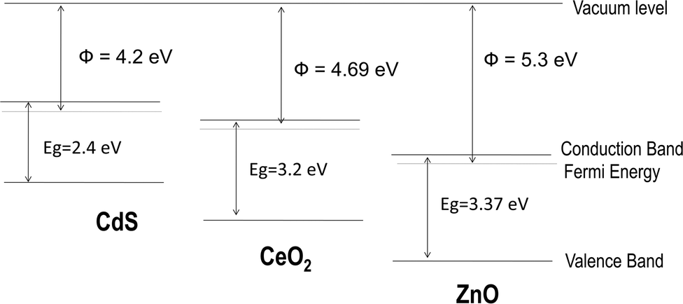 | ||
| Scheme 2 Schematic energy band diagrams of CdS, CeO2 and ZnO. | ||
Owing to the nanometric size of the CdS nanoparticles, the enhanced ‘local’ field (especially in the case of particles present on the edges of the ZnO nanorods) enables them to be active emission sites (Scheme 3). Thus the superior field emission behaviour of the CdS–ZnO heteroarchitecture emitter can be attributed to the combined effect of (i) enhanced electrical conductivity due to electron transfer from CdS particles to ZnO and (ii) increase in the number of emission sites envisaged by the nanometric size of the protruding CdS nanoparticles.
 | ||
| Scheme 3 Schematic representation of enhancement in the field at the tip. | ||
The observed J–E characteristic is further analysed by plotting a graph of ln(J/E2) versus (1/E), known as the Fowler–Nordheim (F–N) plot.37 The F–N plot (inset of Fig. 10) exhibits nonlinear behaviour over the entire range of the applied field, indicating the semiconducting nature of the emitter. Similar nonlinear F–N plots have been reported for ZnO and other semiconductors.38
The emission current versus time (I–t) plots corresponding to various preset values of ~2 μA and 8 μA recorded at a base pressure of 1 × 10⁻⁸ mbar are shown in Fig. 11. The emission current at a higher preset value exhibits a small excursion along with ‘spike’-type fluctuations superimposed on the base level. The spike-type current fluctuations are attributed to adsorption, diffusion/migration, and/or desorption of the residual gas molecules on the emitter surface. Interestingly, the average emission current is seen to remain constant over the entire duration and shows no signs of degradation, which is ascribed to good physical and chemical stability of the emitter. This is a remarkable and promising feature, particularly from the application point of view.
 | ||
| Fig. 11 Field emission current stability (I–t) plot of the CdS–ZnO heteroarchitecture. The inset shows typical field emission images. | ||
Conclusion
In a nutshell, a unique CdS–ZnO heteroarchitecture was synthesized via a facile single-step hydrothermal route. The structural, morphological and optical studies reveal the formation of the CdS–ZnO heteroarchitecture, comprising self-assembled ZnO nanorods decorated with cubic-shaped CdS nanoparticles. The surface modification of ZnO nanorods with CdS leads to a promising field emission behaviour with a low turn-on field value of ~2 V μm−1 (current density ~10 μA cm−2). The CdS–ZnO heteroarchitecture emitter exhibits a high current density of ~1235 μA cm−2 (at ~3.36 V μm−1), which is attributed to the combined effect due to the unique morphology of the heteroarchitecture enabling enhancement in the local electric field, modulation of the work function and electronic properties of ZnO nanorods due to the presence of CdS nanoparticles on their surface. Furthermore, the simple synthesis approach could be explored for the preparation of other heterostructures possessing novel functionalities.Acknowledgements
The authors are thankful to Dr. Satishchandra B. Ogale (NCL, Pune) for assistance in HRTEM analysis. SSW is thankful to Principal (Dr.) S.L. Bonde, Nowrosjee Wadia College, Pune, India, for his research encouragement. A part of the work is supported by the UGC as a DSK postdoctoral fellowship to NSC. Field emission work is carried out as a part of CNQS activity of the Department of Physics, Savitribai Phule Pune University.Notes and references
- J. Y. Lao, J. G. Wen and Z. F. Ren, Nano Lett., 2002, 2, 1287 CrossRef CAS.
- C. Cheng, B. Liu, H. Yang, W. Zhou, L. Sun, R. Chen, S. F. Yu, J. Zhang, H. Gong, H. Sun and H. J. Fan, ACS Nano, 2009, 3, 3069 CrossRef CAS PubMed.
- A. Younis, D. Chu, X. Lin, J. Yi, F. Dang and S. Li, ACS Appl. Mater. Interfaces, 2013, 5, 2249 CAS.
- T. Rakshit, S. P. Mondal, I. Manna and S. K. Ray, ACS Appl. Mater. Interfaces, 2012, 4, 6085 CAS.
- F. Xu, Y. Yuan, H. Han, D. Wu, Z. Gao and K. Jiang, CrystEngComm, 2012, 14, 3615 RSC.
- J. Pan, J. Li, Z. Yan, B. Zhou, H. Wu and X. Xiong, Nanoscale, 2013, 5, 3022 RSC.
- P. Chen, L. Gu and X. Cao, CrystEngComm, 2010, 12, 3950 RSC.
- G. Guerguerian, F. Elhordoy, C. J. Pereyra, R. E. Marotti, F. Martín, D. Leinen, J. R. Ramos-Barrado and E. A. Dalchiele, Nanotechnology, 2011, 22, 505401 CrossRef PubMed.
- U. K. Gautam, X. Fang, Y. Bando, J. Zhan and D. Goldberg, ACS Nano, 2008, 1015 CrossRef CAS PubMed.
- Z. Fang, Y. Liu, Y. Fan, Y. Ni, X. Wei, K. Tang, J. Shen and Y. Chen, J. Phys. Chem. C, 2011, 115, 13968 CAS.
- H. Kim, S. Jeon, M. Lee, J. Lee and K. Yong, J. Mater. Chem., 2011, 21, 13458 RSC.
- F. Zhang, S. Niu, W. Guo, G. Zhu, Y. Liu, X. Zhang and Z. L. Wang, ACS Nano, 2013, 6, 4537 CrossRef PubMed.
- T. Y. Zhai, X. S. Fang, Y. Bando, B. Dierre, B. D. Liu, H. B. Zeng, X. J. Xu, Y. Huang, X. L. Yuan, T. Sekiguchi and D. Golberg, Adv. Funct. Mater., 2009, 19, 2423 CrossRef CAS.
- C. Ye, Y. Bando, X. Fang, G. Shen and D. Golberg, J. Phys. Chem. C, 2007, 111, 12673 CAS.
- T. Zhai, L. Li, Y. Ma, M. Liao, X. Wang, X. Fang, J. Yao, Y. Bando and D. Goldberg, Chem. Soc. Rev., 2011, 40, 2986 RSC.
- D. Ye, S. Moussa, J. D. Ferguson, A. A. Baski and M. S. El-Shall, Nano Lett., 2012, 12, 1265 CrossRef CAS PubMed.
- S. S. Warule, N. S. Chaudhari, R. T. Khare, J. D. Ambekar, B. B. Kale and M. A. More, CrystEngComm, 2013, 15, 7475 RSC.
- S. Xu and Z. L. Wang, Nano Res., 2011, 4, 1013 CrossRef CAS.
- M. Ahmad and J. Zhu, J. Mater. Chem., 2011, 21, 599 RSC.
- P. G. Chavan, S. S. Badadhe, I. S. Mulla, M. A. More and D. S. Joag, Nanoscale, 2011, 3, 1078 RSC.
- F. Zhang, Y. Ding, Y. Zhang, X. Zhang and Z. L. Wang, ACS Nano, 2012, 6, 9229 CrossRef CAS PubMed.
- A. Datta, P. G. Chavan, F. J. Sheini, M. A. More, D. S. Joag and A. Patra, Cryst. Growth Des., 2009, 9, 4157 CAS.
- T. K. Jana, A. Pal and K. Chatterjee, J. Alloys Compd., 2014, 583, 510 CrossRef CAS PubMed.
- S. S. Warule, N. S. Chaudhari, B. B. Kale, K. R. Patil, P. M. Koinkar, M. A. More and R. Murakami, J. Mater. Chem., 2012, 22, 8887 RSC.
- B. X. Lin, Z. X. Fu and Y. B. Jia, Appl. Phys. Lett., 2001, 79, 943 CrossRef CAS PubMed.
- H. Zeng, W. Cai, Y. Li, J. Hu and P. Liu, J. Phys. Chem. B, 2005, 109, 18260 CrossRef CAS PubMed.
- Z. L. Wang, J. Phys.: Condens. Matter, 2004, 16, R829 CrossRef CAS.
- R. Yousefi and B. Kamaluddin, Solid State Sci., 2010, 12, 252 CrossRef CAS PubMed.
- X. H. Huang, C. Zhang, C. B. Tay, T. Venkatesan and S. J. Chua, Appl. Phys. Lett., 2013, 102, 111106 CrossRef PubMed.
- P. Ayyub, P. Vasa, P. Taneja, R. Banerjee and B. P. Singh, J. Appl. Phys., 2005, 97, 104310 CrossRef PubMed.
- J. R. Lakowicz, I. Gryczynski, Z. Gryczynski and C. J. Murphy, J. Phys. Chem. B, 1999, 103, 7613 CrossRef CAS.
- P. Kundu, P. A. Deshpande, G. Madras and N. Ravishankar, J. Mater. Chem., 2011, 21, 4209 RSC.
- J. A. Dean, Lange's Handbook of Chemistry, McGraw-Hill, New York, 1999 Search PubMed.
- S. S. Warule, N. S. Chaudhari, J. D. Ambekar, B. B. Kale and M. A. More, ACS Appl. Mater. Interfaces, 2011, 3, 3454 CAS.
- M. Deo, D. Shinde, A. Yengantiwar, J. Jog, B. Hannoyer, X. Sauvage, M. More and S. Ogale, J. Mater. Chem., 2012, 22, 17055 RSC.
- S. Li, K. Yu, Y. Wang, Z. Zhang, C. Song, H. Yin, Q. Ren and Z. Zhu, CrystEngComm, 2013, 15, 1753 RSC.
- R. H. Fowler and L. W. Nordheim, Proc. R. Soc. London, Ser. A, 1928, 119, 173 CrossRef CAS.
- A. A. Al-Tabbakh, M. A. More, D. S. Joag, I. S. Mulla and V. K. Pillai, ACS Nano, 2010, 4, 5585 CrossRef CAS PubMed.
| This journal is © The Royal Society of Chemistry 2015 |