
 Open Access Article
 This Open Access Article is licensed under a Creative Commons Attribution-Non Commercial 3.0 Unported Licence
Rutile phase n- and p-type anodic titania nanotube arrays with square-shaped pore morphologies†
Piyush
Kar
*a,
Yun
Zhang
a,
Samira
Farsinezhad
a,
Arash
Mohammadpour
a,
Benjamin D.
Wiltshire
a,
Himani
Sharma
 a and
Karthik
Shankar
ab
a and
Karthik
Shankar
ab
aDepartment of Electrical and Computer Engineering, University of Alberta, Edmonton, Alberta T6G2 V4, Canada. E-mail: pkar1@ualberta.ca
bNRC National Institute for Nanotechnology, Edmonton, Alberta T6G 2M9, Canada. E-mail: kshankar@ualberta.ca; Tel: +1 780 492 1354
First published on 31st March 2015
Abstract
Rutile-phase TiO2 nanotube arrays without broken walls were formed by annealing of anodically formed nanotubes in a propane flame at 650 °C and in air at 750 °C. An unusual morphological transformation was observed from the ellipsoidal pore-shapes of titania nanotubes grown in aqueous electrolyte to a square-shaped pore structure subsequent to the anneals. 750 °C annealed nanotubes were found to be lightly p-type, rare in TiO2.
TiO2 nanotube (NT) arrays synthesized by electrochemical anodization are an exciting material platform for photocatalytic, photovoltaic and optoelectronic sensing devices due to their ordered structure, semiconducting behavior, high surface area and also the orthogonalization of light absorption and charge separation intrinsic to their vertically oriented structure. The properties and applications of the rutile-phase anodic TiO2 nanotubes have hitherto been ignored in favor of the lower temperature anatase phase since the formation of rutile required high annealing temperatures which caused destruction of the nanotube structural motif. The nanotubular structure was preserved by us during the heat treatment by use of an optimal annealing regimen. The flame annealing induced transformation of vertically oriented, self-organized TiO2 nanotubes with circular and ellipsoidal cross-sections to TiO2 nanotubes bearing square cross-sections was first noticed by Shankar et al. in 2005;1 however this result was incidental to the 2005 paper and did not receive further study. The technique of flame annealing the titania nanotubes has only been studied in four papers1–4 to the best of our knowledge, and even in these, the focus was on compositional doping effected by the flame annealing process in order to narrow the electronic bandgap. The effect of various annealing treatments on the crystallinity of anodically formed TiO2 nanotubes was studied in a number of articles.5–8 Here, we seek to study the effect of flame annealing on electronic doping by identifying the majority carriers and measuring its concentration in flame annealed TiO2 nanotubes. Reports reproducing square cross-sectioned TiO2 nanotubes are not found in the literature even though the shape of nanostructures is a significant factor affecting wetting behaviour for biomedical and antifouling applications,9,10 small molecule transport through pores for filtration, drug delivery and photocatalytic flow-through membranes,11–13 polymer filling of nanotubes for optoelectronics14,15 and effective refractive index for optical sensing.16 In this study, not only do we generate square-shaped nanotubes but we also determined the phase, carrier concentration and photoelectrochemical properties associated with them. Crystal phase composition dictates performance of nanomaterials in photocatalysis, electrocatalysis and photoelectrochemistry.17–20 For instance, charge separation is stronger in rutile nanoparticles than in anatase nanoparticles.19 Although there has been much debate about the utility of rutile and mixed rutile–anatase phases on the photocatalytic activity (as opposed to pure anatase), most of this work has focused on nanocrystalline titania with only a handful of reports on rutile-phase titania nanotubes.21,22 Here, we report a first study on the potential application of these rutile nanotubes in photoelectrochemical water splitting, where we made a comparison with anatase nanotubes formed under identical anodization conditions.
Low temperature (450 °C) furnace annealed NTs (LANTs) with typical ellipsoidal pore shapes are shown in Fig. 1a. The as-anodized nanotubes have a diameter of 50 nm and a wall thickness of 10 nm. SEM images of high temperature (750 °C) furnace annealed NTs (HANTs) in Fig. 1c and d. HANTs show an average wall spacing of 50 nm and a wall thickness of 20 nm as well as square pores. There is likewise a clear transformation in the morphology of a significant fraction of flame annealed nanotubes (FANTs) from ellipsoidal pores toward square shaped pores, as can be observed in Fig. 1e and f. FANTs have an average wall thickness of 15 nm and an average sidewall breadth of 50 nm. Dimensions of square nanotubes depend on the diameter and height of the precursor LANTs while the spacing between parallel edges of the square nanotubes resembles the inner diameter of the ellipsoidal anatase nanotubes. Cross-sectional FESEM images (Fig. 1b, d and f). Cylindrical cross-sections, 300 nm long nanotubes, characterize LANTs (Fig. 1b). HANTs exhibit 150 nm long square nanotubes (Fig. 1d) and a large barrier layer 750 nm thick, (ESI,† Fig. S3). Profile view of FANTs in Fig. 1f shows a barrier layer (100–150 nm) and a near universal modification of the nanotube cross-sections. In an extension of our flame annealing procedure to ethylene glycol anodized nanotubes (ESI,† Fig. S5), we observed a similar square morphology. In prior reports, ellipsoidal and hexagonal titania nanotubes with broken walls that completely transformed to the rutile phase18,20–22 but did not yield square nanotubes, which indicates the importance of optimal structural and annealing parameters. In furnace annealing, nanotubes do not get heated as rapidly as they do under flame annealing conditions since conduction of heat through the thick titanium foil and the barrier layer of the nanotubes is not as effective a mode of heat transfer as direct heating of the top surface of the nanotubes by a flame. Therefore, as opposed to flame annealing, where shape changes from circular to square nanotubes occur very quickly, i.e. in 20 seconds, furnace based annealing takes a longer time (two hours). The initiation of phase transformation anatase to rutile is believed to occur at rather lower temperatures, e.g. 300 to 500 °C5,23–25 but complete phase transformation requires higher temperatures.
 | ||
| Fig. 1 (a), (c) and (e) Top-view FESEM images of the nanotube samples (a) LANT precursor nanotube samples of ellipsoidal cross-section. (b) HANTs with nearly perfect square pores, and (c) FANTs with pore-shapes intermediate between ellipsoids and squares. (b), (d) and (f) Cross-sectional and profile view FESEM images of the LANTs (d) HANTs (e) and FANTs (f). TiO2 nanotubes are formed by anodization in HF based aqueous electrolyte. Inserted circles clearly indicate square sections. | ||
GIXRD data indicates the predominance of rutile phase for the morphologically transformed nanotubes (i.e. both FANTs and HANTs), as shown in Fig. 2a. The dominant peak in FANTs and HANTs at the 2θ value of 27.445°, which is due to the [110] reflection, confirms rutile as the primary phase constituent. Various other XRD peaks of lower intensity also confirm rutile phase in FANTs and HANTs; specifically these are peaks at 2θ values of 36.1°, 39.2° and 41.2° relating to rutile [101], [200] and [111] planes respectively. From the peak widths shown in the inset of Fig. 2a, the crystallite size was estimated using the Scherrer formula, and was determined to be 21 nm for FANTs and 30 nm for HANTs. The thermodynamically stable rutile phase exhibits Raman active lattice vibrations near 147 cm−1 (B1g), 446 cm−1 (Eg), 610 cm−1 (A1g) and 826 cm−1 (B2g) wave numbers, and a second order band of Raman shift around 230 cm−1, which could be due to a multi-photon process. We measured all the modes except B2g for FANTs and HANTs and observe a highly crystalline rutile phase with a shift in all the peaks (Fig. 2b). Raman-active lattice vibrations for anatase TiO2 are assigned as follows: 147 cm−1 (Eg), 197 cm−1 (Eg), 517 cm−1 (A1g), 397 cm−1 (B1g) and 640 cm−1 (Eg). The decreased intensity of the 148.1 cm−1 peak (red plot) is analogous to rutile TiO2 predomination. However, the presence of low intensity 148.1 cm−1 (which is the main peak of anatase phase) in HANTs and FANTs confirms the presence of a small percentage of anatase phase.
 | ||
| Fig. 2 (a) Peak-indexed GIXRD patterns of LANTs (blue), HANTs (black) and FANTs (red) while the inset is a comparative illustration of the full peak widths at half of maximum intensities of FANTs and HANTs; (b) Raman spectra of LANTs (blue), HANTs (black) and FANTs (red); (c), (d) and (e) TEM lattice images of LANTs, HANTs and FANTs, respectively. | ||
Raman peaks at 426.5 and 444.74 cm−1 (Fig. 2b), which conform to the Eg mode for FANTs and HANTs, respectively, are blue-shifted. The magnitude of the blue-shift may be attributed to crystallite size.26 Here it is observed that FANTs which have a smaller crystallite size than HANTs, as inferred from the full-width at half maximum (FWHM) data in Fig. 2a, exhibit Eg modes that are less blue-shifted than the same exhibited by HANTs. In addition to crystallite size, lattice strain and defect affect Raman peak shifting, broadening, and intensity,27 which are attributed to the presence of asymmetric structures, typically Ti–O bonds28 causing softening of the Eg mode. The Raman data (Fig. 2b) is consistent with the XRD data (Fig. 2a) for the three nanotube types. This is because the Raman peaks for FANTs and HANTs at 426.5 and 444.74 cm−1, which represent the Eg mode, are caused by the symmetric stretching vibration of the stoichiometric O–Ti–O bonds present in the predominant rutile TiO2 (110) planes. Likewise, the Raman peak near 148.1 cm−1 represents the Eg mode that corresponds to the predominant anatase (101) planes.29 TEM lattice images, with d-spacings, for LANTs, HANTs and FANTs are shown in Fig. 2c–e respectively. Our d-spacings are very close to literature reported values, with less than 5% variance. We measured the d-spacing for LANTs (Fig. 2c) to be 4.51 Å which corresponds to anatase (002), and 3.12 Å and 3.22 Å which correspond to anatase (101).30 For HANTs, d-spacings of 2.17 and 2.40 Å correspond to rutile (110) and rutile (101), respectively.31 For FANTs, d-spacing is 3.15 Å that corresponds to rutile (110),31,32 2.37 and 2.40 Å which correspond to rutile (101),33 and 2.79 Å and 2.93 Å that correspond to rutile (001).34 TEM lattice images also indicate that all three types of nanotubes are polycrystalline, and the crystallite size, as observed, is smaller for FANTs than the HANTs, which is consistent with findings from XRD data.
XPS data reveals predominantly TiO2 stoichiometry. Fig. 3a shows Ti 2p3/2 peaks at 459.3 eV and Ti 2p1/2 at 465 eV, and Fig. 3b shows O 1s peaks 530.6 eV.35 The binding energy for F 1s peaks were between 683 and 685 eV (Fig. 3c). F 1s intensity is the most for LANTs and the least for HANTs, which is consistent with annealing intensity.24 Fig. S6 (ESI†) indicates presence adsorbed nitrogen (peak at 400 eV36) in all three types of nanotubes but indicates presence of bonded nitrogen (peak at 396 eV37) in HANTs only.
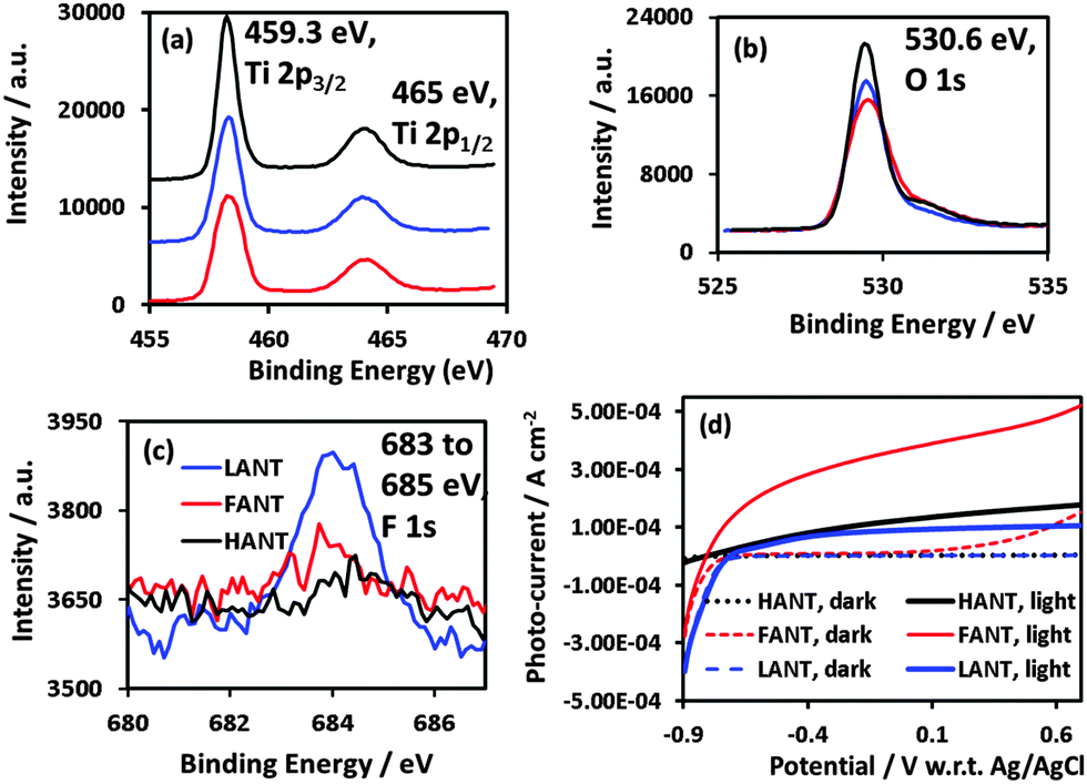 | ||
| Fig. 3 (a), (b), and (c) represent XPS spectra for Ti 2p, O 1s, and F 1s, respectively, and (d) shows the plots of photocurrent versus potential under dark and under AM 1.5G simulated sunlight, for the three types of nanotubes. | ||
EIS analysis, including representative Nyquist plots, is included in the ESI† (Fig. S7). HANTs exhibit very low capacitance and high transport resistance, which we relate to their thick barrier layer. On the other hand, FANTs and LANTs each exhibit a much higher capacitance and a charge carrier transport resistance that is a few orders of magnitude lower. The Mott–Schottky plots (Fig. S7a, ESI†) confirmed n-type character for FANTs with a carrier concentration of 1.5 × 1018 cm−3 and a flat band potential of −0.67 V w.r.t. Ag/AgCl were obtained while for LANTs, a flat band potential of −0.5 V (w.r.t. Ag/AgCl) and carrier concentration of 7.0 × 1019 cm−3 were obtained. The extracted parameters for LANTs are in agreement with other reported measurements of flat band potential and carrier concentration.38,39 In Fig. S8c (ESI†), the flat band potential was found to be 0.4 V vs. Ag/AgCl for HANTs. These results can be understood considering that mobile charge carriers in anatase phase LANTs and rutile phase FANTs arise due to oxygen vacancies, or point defects. In case of the rutile phase HANTs, the charge carriers are titanium vacancies caused by oxygenation under exposure to air at 750 °C. While large bandgap semiconductors are difficult to dope p-type, previous reports40–42 have confirmed the possibility of forming p-type rutile. p-Type TiO2 films are exciting because while difficult to obtain, they extend the application spectrum of n-type TiO2 by enabling transparent and high power homojunction diodes, new photocatalytic configurations to exploit the reducing behavior of excess electrons and heterojunction solar cells based on n-type absorbers and a p-type TiO2 scaffold.43 This work demonstrates a solution-based synthetic route for p-type TiO2 nanostructures that does not involve doping by metal ions. Characteristics of the three types of nanotubes are summarized in Table S1 in the ESI.†
The photoelectrochemical performance in 1 M KOH under AM 1.5 one sun illumination, shown in Fig. 3d, is the highest for FANTs followed by HANTs and then by LANTs. The photocurrent density exhibited by FANTs is comparable to the highest reported values for aqueous TiO2 nanotubes, without the aid of co-catalysts. As prior reports have shown,44,45 doping-induced bandgap narrowing is not responsible. The contributing factors are primarily (i) the high degree of rutile crystallinity of FANTs which increases light harvesting due to both the higher absorption coefficient of rutile for ultraviolet photons coupled with a lower bandgap than anatase (3.0 eV vs. 3.2 eV)46 (ii) a lower charge carrier transport resistance as shown in Fig. S2f in the ESI† than LANTs at applied potentials above −0.7 V (w.r.t. Ag/AgCl) and (iii) a lower electron concentration which allows for a higher sensitivity of the Fermi level to the applied potential as well as lower geminate recombination. From an electrochemical standpoint, the open-circuit potential for FANTs is lower than that for LANTs enabling higher photo-electrochemical yield. HANTs on the other hand perform the poorest and we attribute this directly to the thick barrier layer seen in Fig. 1d due to which charge carriers are produced at a distance farther than a retrieval length (sum of depletion layer + hole diffusion length) from the electrolyte interface.47
Flame annealing and furnace annealing of nanotubes grown anodically in aqueous electrolytes produced the morphological transformation from ellipsoidal pores to square-shaped pores together with phase transformation from anatase to rutile. XRD, Raman and TEM data clearly demonstrate consistency of phase composition of the three types of nanotubes. XPS analysis shows stoichiometric TiO2 for the nanotubes with no peak shifts, whereby it is also shown that fluoride concentration decreased with intensity of annealing. Mott Schottky analysis revealed n-type conduction in the flame-annealed rutile TiO2 nanotubes, and p-type conduction in furnace-annealed rutile TiO2 nanotubes. Electron concentration in flame-annealed rutile nanotubes was determined to be 1.5 × 1018 cm−3, while the hole concentration in furnace annealed rutile nanotubes was 2.8 × 1012 cm−3. Photoelectrochemical performance, measured in terms of photocurrent density, is the highest using flame annealed TiO2 nanotubes as compared to 750 °C furnace annealed nanotubes and anatase nanotubes formed under identical anodization conditions.
The authors thank NSERC, CFI, NRC-NINT and CMC Microsystems for direct or indirect funding support. S.F. thanks Alberta Innovates Technology Futures for scholarship support. P.K. thanks Shiraz Merali for help with XRD.
Notes and references
- K. Shankar, M. Paulose, G. K. Mor, O. K. Varghese and C. A. Grimes, J. Phys. D: Appl. Phys., 2005, 38, 3543–3549 CrossRef CAS.
- C. K. Xu, Y. A. Shaban, W. B. Ingler and S. U. M. Khan, Sol. Energy Mater. Sol. Cells, 2007, 91, 938–943 CrossRef CAS PubMed.
- A. Mazare, I. Paramasivam, K. Lee and P. Schmuki, Electrochem. Commun., 2011, 13, 1030–1034 CrossRef CAS PubMed.
- A. Mazare, I. Paramasivam, F. Schmidt-Stein, K. Lee, I. Demetrescu and P. Schmuki, Electrochim. Acta, 2012, 66, 12–21 CrossRef CAS PubMed.
- O. K. Varghese, D. W. Gong, M. Paulose, C. A. Grimes and E. C. Dickey, J. Mater. Res., 2003, 18, 156–165 CrossRef CAS.
- A. Ghicov, H. Tsuchiya, J. M. Macak and P. Schmuki, Phys. Status Solidi A, 2006, 203, R28–R30 CrossRef CAS.
- A. Tighineanu, S. P. Albu and P. Schmuki, Phys. Status Solidi RRL, 2014, 8, 158–162 CrossRef CAS.
- R. Hahn, A. Ghicov, J. Salonen, V. P. Lehto and P. Schmuki, Nanotechnology, 2007, 18, 105604 CrossRef.
- S. Farsinezhad, P. R. Waghmare, B. D. Wiltshire, H. Sharma, S. Amiri, S. K. Mitra and K. Shankar, RSC Adv., 2014, 4, 33587–33598 RSC.
- P. Kar and K. Shankar, J. Nanosci. Nanotechnol., 2013, 13, 4473–4496 CrossRef CAS PubMed.
- M. Paulose, L. Peng, K. C. Popat, O. K. Varghese, T. J. LaTempa, N. Z. Bao, T. A. Desai and C. A. Grimes, J. Membr. Sci., 2008, 319, 199–205 CrossRef CAS PubMed.
- D. Losic and S. Simovic, Expert Opin. Drug Delivery, 2009, 6, 1363–1381 CrossRef CAS PubMed.
- S. P. Albu, A. Ghicov, J. M. Macak, R. Hahn and P. Schmuki, Nano Lett., 2007, 7, 1286–1289 CrossRef CAS PubMed.
- S. Kim, G. K. Mor, M. Paulose, O. K. Varghese, K. Shankar and C. A. Grimes, IEEE J. Sel. Top. Quantum Electron., 2010, 16, 1573–1580 CrossRef CAS.
- K. Shankar, G. K. Mor, M. Paulose, O. K. Varghese and C. A. Grimes, J. Non-Cryst. Solids, 2008, 354, 2767–2771 CrossRef CAS PubMed.
- K. S. Mun, S. D. Alvarez, W. Y. Choi and M. J. Sailor, ACS Nano, 2010, 4, 2070–2076 CrossRef CAS PubMed.
- D. A. Wang, Y. Liu, B. Yu, F. Zhou and W. M. Liu, Chem. Mater., 2009, 21, 1198–1206 CrossRef CAS.
- T. Ohno, K. Sarukawa and M. Matsumura, New J. Chem., 2002, 26, 1167–1170 RSC.
- T. Ohno, K. Sarukawa, K. Tokieda and M. Matsumura, J. Catal., 2001, 203, 82–86 CrossRef CAS.
- S. Yurdakal, G. Palmisano, V. Loddo, V. Augugliaro and L. Palmisano, J. Am. Chem. Soc., 2008, 130, 1568–1569 CrossRef CAS PubMed.
- Y. Bai, S. Park, H. H. Park, M. H. Lee, T. S. Bae, W. Duncan and A. Swain, Surf. Interface Anal., 2011, 43, 998–1005 CrossRef CAS.
- D. Eder, I. A. Kinloch and A. H. Windle, Chem. Commun., 2006, 1448–1450 RSC.
- S. Sreekantan, R. Hazan and Z. Lockman, Thin Solid Films, 2009, 518, 16–21 CrossRef CAS PubMed.
- D. Regonini, A. Jaroenworaluck, R. Stevens and C. R. Bowen, Surf. Interface Anal., 2010, 42, 139–144 CrossRef CAS.
- P. Kar, K. S. Raja, M. Misra and B. N. Agasanapur, Mater. Res. Bull., 2009, 44, 398–402 CrossRef CAS PubMed.
- W. F. Zhang, Y. L. He, M. S. Zhang, Z. Yin and Q. Chen, J. Phys. D: Appl. Phys., 2000, 33, 912–916 CrossRef CAS.
- S. K. Gautam, F. Singh, I. Sulania, R. G. Singh, P. K. Kulriya and E. Pippel, J. Appl. Phys., 2014, 115, 143504 CrossRef PubMed.
- N. Nakanishi, A. Nagasawa and Y. Murakami, Journal De Physique, 1982, 43, 35–55 Search PubMed.
- J. Yan, G. Wu, N. Guan, L. Li, Z. Li and X. Cao, Phys. Chem. Chem. Phys., 2013, 15, 10978–10988 RSC.
- L. Miao, S. Tanemura, P. Jin, K. Kaneko, A. Terai and N. Nabatova-Gabain, J. Cryst. Growth, 2003, 254, 100–106 CrossRef CAS.
- C. Williams, Proc. R. Soc. London, Ser. A, 1917, 93, 418–427 CrossRef CAS.
- K. Thamaphat, P. Limsuwan and B. Ngotawornchai, Kasetsart J.: Nat. Sci., 2008, 42, 357–361 Search PubMed.
- L. Miao, P. Jin, K. Kaneko, A. Terai, N. Nabatova-Gabain and S. Tanemura, Appl. Surf. Sci., 2003, 212–213, 255–263 CrossRef CAS.
- W. Guo, C. Xu, X. Wang, S. Wang, C. Pan, C. Lin and Z. L. Wang, J. Am. Chem. Soc., 2012, 134, 4437–4441 CrossRef CAS PubMed.
- Y. Lai, L. Sun, Y. Chen, H. Zhuang, C. Lin and J. W. Chin, J. Electrochem. Soc., 2006, 153, D123–D127 CrossRef CAS PubMed.
- A. Ghicov, J. M. Macak, H. Tsuchiya, J. Kunze, V. Haeublein, L. Frey and P. Schmuki, Nano Lett., 2006, 6, 1080–1082 CrossRef CAS.
- N. C. Saha and H. G. Tompkins, J. Appl. Phys., 1992, 72, 3072–3079 CrossRef CAS PubMed.
- A. G. Munoz, Electrochim. Acta, 2007, 52, 4167–4176 CrossRef CAS PubMed.
- V. K. Mahajan, S. K. Mohapatra and M. Misra, Int. J. Hydrogen Energy, 2008, 33, 5369–5374 CrossRef CAS PubMed.
- A. Matsushita, M. Shimoda, T. Naka and Y. Yamada, Jpn. J. Appl. Phys., 2011, 50, 025501 CrossRef.
- N. Savage, B. Chwieroth, A. Ginwalla, B. R. Patton, S. A. Akbar and P. K. Dutta, Sens. Actuators, B, 2001, 79, 17–27 CrossRef CAS.
- S. Erdal, C. Kongshaug, T. S. Bjorheim, N. Jalarvo, R. Haugsrud and T. Norby, J. Phys. Chem. C, 2010, 114, 9139–9145 CAS.
- A. T. Iancu, M. Logar, J. Park and F. B. Prinz, ACS Appl. Mater. Interfaces, 2015, 7, 5134–5140 CAS.
- J. Wang, D. N. Tafen, J. P. Lewis, Z. L. Hong, A. Manivannan, M. J. Zhi, M. Li and N. Q. Wu, J. Am. Chem. Soc., 2009, 131, 12290–12297 CrossRef CAS PubMed.
- J. Zhong, F. Chen and J. L. Zhang, J. Phys. Chem. C, 2010, 114, 933–939 CAS.
- G. E. Jellison, L. A. Boatner, J. D. Budai, B. S. Jeong and D. P. Norton, J. Appl. Phys., 2003, 93, 9537–9541 CrossRef CAS PubMed.
- J. vandeLagemaat, M. Plakman, D. Vanmaekelbergh and J. J. Kelly, Appl. Phys. Lett., 1996, 69, 2246–2248 CrossRef CAS PubMed.
Footnote |
| † Electronic supplementary information (ESI) available: Experimental details, additional electron micrographs, EIS modeling and exracted parameters. See DOI: 10.1039/c5cc01829c |
| This journal is © The Royal Society of Chemistry 2015 |