
 Open Access Article
 This Open Access Article is licensed under a
 Creative Commons Attribution 3.0 Unported Licence
Perovskite solar cells prepared by flash evaporation
Giulia
Longo
,
Lidón
Gil-Escrig
,
Maarten J.
Degen
,
Michele
Sessolo
and
Henk J.
Bolink
*
Instituto de Ciencia Molecular, Universidad de Valencia, c/Catedrático J. Beltrán, 2, 46980 Paterna, Spain. E-mail: henk.bolink@uv.es; Fax: +34-963543273; Tel: +34-963544416
First published on 25th March 2015
Abstract
A simple vacuum deposition method for the preparation of high quality hybrid organic–inorganic methylammonium lead iodide perovskite thin films is reported. When sandwiched in between organic charge transporting layers, such films lead to solar cells with a power conversion efficiency of 12.2%.
Organic–inorganic (hybrid) halide perovskites consisting of aliphatic or aromatic ammonium cations and divalent metals have been the focus of several studies due to their interesting optoelectronic properties, high charge mobility and ease of deposition even through solution-based methods.1,2 More recently, three dimensional hybrid perovskites have been successfully employed as light harvesters in thin film solar cells.3,4 Thanks to a large scientific effort by a number of research groups, the device performance has seen a spectacular rise and, in only five years, a record power conversion efficiency (PCE) as high as 20.1% has been reported.5–14 Early studies focused mainly on the optimization of the solar cell architecture through interface engineering, i.e. choice of proper hole transport materials (HTMs),4,9,15,16 and electron transport materials (ETMs).3,8,12,17,18 Most recent investigations, however, have demonstrated that the control over the perovskite crystallization plays a main role in the achievement of high PCE devices.19,20 Homogeneous perovskite films with large crystal size are desirable since they would allow to increase the layer thickness, thus increasing the sunlight absorption, without hindering the charge transport and collection. Many different strategies have been proposed so far for the solution-processing of hybrid perovskites.21–26 Besides the deeper understanding on the structure–properties relation in methylammonium lead halide perovskite cells, these studies also highlighted the complexity and interplay of parameters involved in the solution deposition of such materials. Taking into account that perovskite solar cells are potential candidate for complementing silicon or copper indium gallium selenide (CIGS) cells in tandem devices, the development of a reliable and thin-film compatible deposition technique is a primary task. Within this perspective, dual source vapour deposition has been proposed as an attractive alternative in the preparation of CH3NH3PbI3 thin films for photovoltaics.7,12 Perovskites layers were obtained by simultaneous controlled co-evaporation of the lead halide (either PbCl2 or PbI2) and the methylammonium iodide CH3NH3I (MAI) in high vacuum chambers. Such vapour-deposited films are very flat and homogeneous and, when employed in solar cells architecture, lead to PCEs as high as 16.5%.27 Co-evaporation enables a fine control over the stoichiometry and thickness of the perovskite films, and takes advantage of the intrinsic high purity of sublimated compounds. Moreover, the technique allows for the preparation of multi-layer stacks, and is fully compatible with standard semiconductor processing. On the other side, the process is relatively time-consuming and it requires accurate periodical calibrations to properly control the deposition rate and precursors ratio. An alternative physical method for the deposition of compound semiconductors is flash evaporation.28,29 The material to be deposited is placed on a metal heater and brought to vacuum, and then a large current is passed through the heater causing the material to rapidly evaporate and condense onto a substrate. Layered, 2D perovskite metal halide doped with aliphatic or aromatic ammonium cations were deposited with this method, resulting in optically active, polycrystalline thin films.30 The desired hybrid film is formed at temperatures high enough for the inorganic compound to evaporate, without causing the decomposition of the organic component.31
In this communication, we report the flash evaporation of 3D organic–inorganic hybrid perovskites and their use in efficient, planar photovoltaic devices. We show that uniform and smooth polycrystalline CH3NH3PbI3 thin films of the desired thickness can be obtained by careful tuning of the deposition parameters. The as-deposited material was characterized by optical and morphological methods, revealing a high degree of homogeneity as well as a low surface roughness, which is desirable for its implementation into optoelectronic devices. The photovoltaic properties of flash evaporated CH3NH3PbI3 thin films were evaluated in planar heterojunction solar cells employing organic charge transport layers. High PCE up to 12% were obtained, demonstrating the potential of flash evaporation as an alternative method for the production of efficient perovskite solar cells. While the flash evaporation technique allows for the deposition of hybrid perovskite films even from their powders as the precursor, we found that a better control over the thickness and homogeneity of the final layer is obtained if the metal heater is coated with the material to be deposited.
The MAI was synthetized according to a previously published method32 and dried at 60 °C in vacuum for 24 hours. A 50 wt% perovskite precursor solution is prepared by dissolving PbI2 (Sigma Aldrich) and MAI in DMF, with a molar ratio PbI2![[thin space (1/6-em)]](https://www.rsc.org/images/entities/char_2009.gif) :MAI of about 1:3. The solution is subsequently deposited onto the metal heater (a tantalum foil of 70 × 15 × 0.05 mm) by meniscus coating (Fig. 1a).33 The layer is created by placing 80 μl of precursor solution under the metal blade (1.2 mm high) and by spreading it over the tantalum foil at a speed of 80 mm s−1. During deposition the foil is heated at 80 °C and once the perovskite layer forms (i.e. the layer turns from yellow to dark brown, Fig. 1b), it is heated at 125 °C for 5 minutes in order to remove the excess solvent. The tantalum foil is subsequently transferred into a high vacuum chamber and clamped in between two electrodes connected to a high current source (Fig. 1c). The substrates to be coated are placed on a sample holder mounted at a vertical distance of 10 cm from the evaporation source. After establishing a stationary vacuum of approximately 0.1 mbar, a large current (approximately 30 A) is passed through the tantalum foil, causing the complete and virtually instantaneous evaporation of the CH3NH3PbI3. The resulting film thickness is controlled by the amount of perovskite initially deposited on the metal heater. The grazing incident X-ray diffraction (GIXRD) pattern of an as-deposited 200 nm thick film is reported in Fig. 2a. The spectrum suggests a high degree of crystallinity, with the peaks at 14.1°, 28.4° and 31.8° confirming the formation of the tetragonal structure of the MAPbI3 perovskite. The surface topography of the film was also investigated by atomic force microscopy (AFM, Fig. 2b). The film shows homogenous aggregation and is relatively flat, with a root mean square (RMS) roughness, calculated over an area of 25 μm2, of 17.6 nm. These data demonstrate that a 3D hybrid organic–inorganic perovskite can be evaporated and reassembled onto a desired substrate with a high degree of crystallinity and homogeneous morphology. These characteristics are of particular interest for optoelectronic applications such as thin film photovoltaic devices. Single junction solar cell were prepared by integration of the perovskite films in a multilayer stack of organic semiconducting layers. Indium tin oxide (ITO) coated glass slides were used as bottom transparent electrode.
:MAI of about 1:3. The solution is subsequently deposited onto the metal heater (a tantalum foil of 70 × 15 × 0.05 mm) by meniscus coating (Fig. 1a).33 The layer is created by placing 80 μl of precursor solution under the metal blade (1.2 mm high) and by spreading it over the tantalum foil at a speed of 80 mm s−1. During deposition the foil is heated at 80 °C and once the perovskite layer forms (i.e. the layer turns from yellow to dark brown, Fig. 1b), it is heated at 125 °C for 5 minutes in order to remove the excess solvent. The tantalum foil is subsequently transferred into a high vacuum chamber and clamped in between two electrodes connected to a high current source (Fig. 1c). The substrates to be coated are placed on a sample holder mounted at a vertical distance of 10 cm from the evaporation source. After establishing a stationary vacuum of approximately 0.1 mbar, a large current (approximately 30 A) is passed through the tantalum foil, causing the complete and virtually instantaneous evaporation of the CH3NH3PbI3. The resulting film thickness is controlled by the amount of perovskite initially deposited on the metal heater. The grazing incident X-ray diffraction (GIXRD) pattern of an as-deposited 200 nm thick film is reported in Fig. 2a. The spectrum suggests a high degree of crystallinity, with the peaks at 14.1°, 28.4° and 31.8° confirming the formation of the tetragonal structure of the MAPbI3 perovskite. The surface topography of the film was also investigated by atomic force microscopy (AFM, Fig. 2b). The film shows homogenous aggregation and is relatively flat, with a root mean square (RMS) roughness, calculated over an area of 25 μm2, of 17.6 nm. These data demonstrate that a 3D hybrid organic–inorganic perovskite can be evaporated and reassembled onto a desired substrate with a high degree of crystallinity and homogeneous morphology. These characteristics are of particular interest for optoelectronic applications such as thin film photovoltaic devices. Single junction solar cell were prepared by integration of the perovskite films in a multilayer stack of organic semiconducting layers. Indium tin oxide (ITO) coated glass slides were used as bottom transparent electrode.
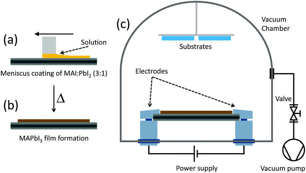 | ||
| Fig. 1 Process flow for the deposition of hybrid organic–inorganic perovskite thin films via flash evaporation. (a) The precursor solution is spread onto a tantalum foil via meniscus coating and (b) annealed to obtain a polycrystalline CH3NH3PbI3 film. The coated tantalum sheet is then transferred to a vacuum chamber (c) where the hybrid perovskite is evaporated onto the desired substrate. | ||
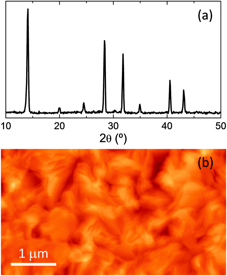 | ||
| Fig. 2 (a) GIXRD pattern and (b) AFM topography of a CH3NH3PbI3 thin film deposited by flash evaporation. | ||
An 80 nm thick of poly(3,4-ethylenedioxythiophene) doped with poly(styrenesulfonate) (PEDOT:PSS, Heraeus Clevios™ P VP AI 4083) was spin-coated onto the ITO and used as the hole injection layer (HIL). After annealing it at 150 °C for 15 minutes, a 20 nm thick poly(N,N′-bis(4-butylphenyl)-N,N′-bis(phenyl)benzidine) (polyTPD) HTL was deposited on top from chlorobenzene (1 wt%) and annealed at 180 °C for 30 s. The polymer stack was subsequently transferred to the vacuum chamber and a 200 nm thick film of MAPbI3 perovskite was deposited by flash evaporation. The stack was completed by spin-coating an 80 nm thick (6,6)-phenyl C61-butyric acid methyl ester (PCBM) thin film and with the thermal vacuum deposition of a bilayer cathode composed of Ba and Ag (10 and 100 nm, respectively). The device characterization was performed in a nitrogen glove box, using a mini-sun simulator designed by ECN and calibrated with a Si reference cell. The device EQE as well as the perovskite film UV-visible absorption spectrum are reported in Fig. 3a. The optical absorption shows the typical profile of the MAPbI3 perovskite, with a broad absorption over the whole visible spectrum and onset at about 800 nm, corresponding to an optical band gap of 1.55 eV. The EQE rises at the same wavelength, reaching a maximum value of 73% in the green (570 nm) and in the blue (420–450 nm) region of the spectrum. The current density–voltage (J–V) characteristic of the solar cell is reported in Fig. 3b. The J–V curve is almost independent on the scan direction, in contrary to what often observed for solution-processed perovskite devices. The short-circuit current density (JSC), open-circuit voltage (VOC) and fill factor (FF) for a typical device, are 18.0 mA cm−2, 1.07 V and 68%, respectively, leading to a remarkable power conversion efficiency of 12.2%. This result is of great importance for the future development of photovoltaic devices based on hybrid organic–inorganic perovskite materials, especially in view of their integration with existing thin film photovoltaic technologies. The deposition process is scalable, additive and extremely fast (in the order of few seconds), which is desirable for the implementation of this materials in industrial applications.
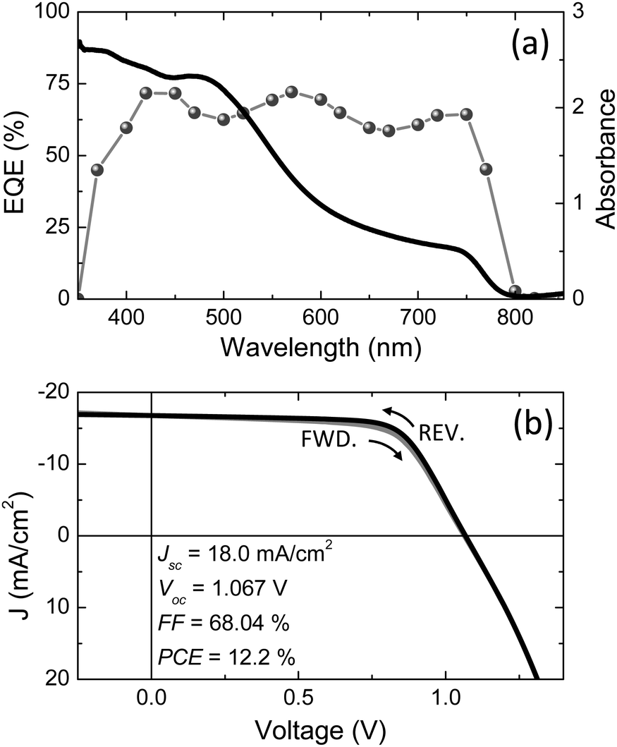 | ||
| Fig. 3 (a) EQE (symbols) and optical absorption (line) in the UV-visible region for a planar perovskite solar cell and its active layer, respectively, deposited by flash evaporation. (b) J–V curve in forward (FWD.) and reverse (REV.) bias for a device under illumination with the structure ITO/PEDOT:PSS/polyTPD/MAPbI3/PCBM/Ba/Ag. The scan rate in both bias direction was 0.1 V s−1. | ||
In summary, 3D methylammonium lead iodide perovskites have been prepared by flash evaporation. Homogeneous and highly crystalline thin films can be obtained with unique control over the material composition and film thickness. The as-deposited films have been tested in planar solar cells employing organic charge transport layers, demonstrating power conversion efficiencies exceeding 12%. This method allows for a straight-forward preparation of multi-layer structures of different organic–inorganic materials, which are foreseen as the big challenge in hybrid perovskite devices. Moreover, the simplicity of the process is particularly suited for the preparation of tandem solar cells, where the perovskite device could be used as a top transparent device in silicon or CIGS photovoltaic modules.
Notes and references
- C. R. Kagan, D. B. Mitzi and C. D. Dimitrakopoulos, Science, 1999, 286, 945–947 CrossRef CAS.
- D. B. Mitzi, C. A. Feild, W. T. A. Harrison and A. M. Guloy, Nature, 1994, 369, 467–469 CrossRef CAS.
- A. Kojima, K. Teshima, Y. Shirai and T. Miyasaka, J. Am. Chem. Soc., 2009, 131, 6050–6051 CrossRef CAS PubMed.
- M. M. Lee, J. Teuscher, T. Miyasaka, T. N. Murakami and H. J. Snaith, Science, 2012, 338, 643–647 CrossRef CAS PubMed.
- H. J. Snaith, J. Phys. Chem. Lett., 2013, 4, 3623–3630 CrossRef CAS.
- N. G. Park, J. Phys. Chem. Lett., 2013, 4, 2423–2429 CrossRef CAS.
- M. Liu, M. B. Johnston and H. J. Snaith, Nature, 2013, 501, 395–398 CrossRef CAS PubMed.
- H. Zhou, Q. Chen, G. Li, S. Luo, T. B. Song, H. S. Duan, Z. Hong, J. You, Y. Liu and Y. Yang, Science, 2014, 345, 542–546 CrossRef CAS PubMed.
- P. Gao, M. Grätzel and M. K. Nazeeruddin, Energy Environ. Sci., 2014, 7, 2448–2463 CAS.
- S. Kazim, M. K. Nazeeruddin, M. Grätzel and S. Ahmad, Angew. Chem., Int. Ed., 2014, 53, 2812–2824 CrossRef CAS PubMed.
- P. P. Boix, K. Nonomura, N. Mathews and S. G. Mhaisalkar, Mater. Today, 2014, 17, 16–23 CrossRef CAS PubMed.
- O. Malinkiewicz, A. Yella, Y. H. Lee, G. M. Espallargas, M. Graetzel, M. K. Nazeeruddin and H. J. Bolink, Nat. Photonics, 2014, 8, 128–132 CrossRef CAS.
- M. Gratzel, Nat. Mater., 2014, 13, 838–842 CrossRef CAS PubMed.
- M. A. Green, K. Emery, Y. Hishikawa, W. Warta and E. D. Dunlop, Prog. Photovolt.: Res. Appl., 2015, 23, 1–9 CrossRef PubMed.
- P. Qin, S. Tanaka, S. Ito, N. Tetreault, K. Manabe, H. Nishino, M. K. Nazeeruddin and M. Grätzel, Nat. Commun., 2014, 5, 3834 CAS.
- J. Y. Jeng, K. C. Chen, T. Y. Chiang, P. Y. Lin, T. D. Tsai, Y. C. Chang, T. F. Guo, P. Chen, T. C. Wen and Y. J. Hsu, Adv. Mater., 2014, 26, 4107–4113 CrossRef CAS PubMed.
- A. Mei, X. Li, L. Liu, Z. Ku, T. Liu, Y. Rong, M. Xu, M. Hu, J. Chen, Y. Yang, M. Grätzel and H. Han, Science, 2014, 345, 295–298 CrossRef CAS PubMed.
- J. Y. Jeng, Y. F. Chiang, M. H. Lee, S. R. Peng, T. F. Guo, P. Chen and T. C. Wen, Adv. Mater., 2013, 25, 3727–3732 CrossRef CAS PubMed.
- W. Nie, H. Tsai, R. Asadpour, J.-C. Blancon, A. J. Neukirch, G. Gupta, J. J. Crochet, M. Chhowalla, S. Tretiak, M. A. Alam, H.-L. Wang and A. D. Mohite, Science, 2015, 347, 522–525 CrossRef CAS PubMed.
- D. Shi, V. Adinolfi, R. Comin, M. Yuan, E. Alarousu, A. Buin, Y. Chen, S. Hoogland, A. Rothenberger, K. Katsiev, Y. Losovyj, X. Zhang, P. A. Dowben, O. F. Mohammed, E. H. Sargent and O. M. Bakr, Science, 2015, 347, 519–522 CrossRef CAS PubMed.
- J. Burschka, N. Pellet, S. J. Moon, R. Humphry-Baker, P. Gao, M. K. Nazeeruddin and M. Grätzel, Nature, 2013, 499, 316–319 CrossRef CAS PubMed.
- Q. Chen, H. Zhou, Z. Hong, S. Luo, H. S. Duan, H. H. Wang, Y. Liu, G. Li and Y. Yang, J. Am. Chem. Soc., 2014, 136, 622–625 CrossRef CAS PubMed.
- A. Dualeh, N. Tétreault, T. Moehl, P. Gao, M. K. Nazeeruddin and M. Grätzel, Adv. Funct. Mater., 2014, 24, 3250–3258 CrossRef CAS PubMed.
- G. E. Eperon, V. M. Burlakov, P. Docampo, A. Goriely and H. J. Snaith, Adv. Funct. Mater., 2014, 24, 151–157 CrossRef CAS PubMed.
- Z. Xiao, Q. Dong, C. Bi, Y. Shao, Y. Yuan and J. Huang, Adv. Mater., 2014, 26, 6503–6509 CrossRef CAS PubMed.
- N. J. Jeon, J. H. Noh, Y. C. Kim, W. S. Yang, S. Ryu and S. I. Seok, Nat. Mater., 2014, 13, 897–903 CrossRef CAS PubMed.
- Q. Lin, A. Armin, R. C. R. Nagiri, P. L. Burn and P. Meredith, Nat. Photonics, 2015, 9, 106–112 CrossRef CAS.
- L. Harris and B. M. Siegel, J. Appl. Phys., 1948, 19, 739–741 CrossRef CAS PubMed.
- J. L. Richards, P. B. Hart and L. M. Gallone, J. Appl. Phys., 1963, 34, 3418–3420 CrossRef CAS PubMed.
- D. B. Mitzi, M. T. Prikas and K. Chondroudis, Chem. Mater., 1999, 11, 542–544 CrossRef CAS.
- K. Chondroudis, D. B. Mitzi and P. Brock, Chem. Mater., 1999, 12, 169–175 CrossRef.
- L. Etgar, P. Gao, Z. Xue, Q. Peng, A. K. Chandiran, B. Liu, M. K. Nazeeruddin and M. Grätzel, J. Am. Chem. Soc., 2012, 134, 17396–17399 CrossRef CAS PubMed.
- C. S. Herrick, Ind. Eng. Chem. Prod. Res. Dev., 1980, 19, 314–316 CrossRef CAS.
| This journal is © The Royal Society of Chemistry 2015 |