
 Open Access Article
 This Open Access Article is licensed under a
 Creative Commons Attribution 3.0 Unported Licence
An N-ethylated barbituric acid end-capped bithiophene as an electron-acceptor material in fullerene-free organic photovoltaics†
Paul
Sullivan
*a,
Gavin E.
Collis
*b,
Luke A.
Rochford
a,
Junior Ferreira
Arantes
b,
Peter
Kemppinen
b,
Tim S.
Jones
a and
Kevin N.
Winzenberg
b
aDepartment of Chemistry, University of Warwick, Coventry, CV4 7AL, UK. E-mail: p.j.sullivan@warwick.ac.uk; Tel: +44 (0)2476 522188
bAdvanced Fibres and Chemical Industries, CSIRO Manufacturing Flagship, Melbourne, Private Bag 10, VIC 3169, Australia. E-mail: Gavin.Collis@csiro.au; Tel: +61 3 9545 2458
First published on 5th March 2015
Abstract
A new evaporable electron acceptor material for organic photovoltaics based on N-ethyl barbituric acid bithiophene (EBB) has been demonstrated. Bilayer devices fabricated with this non-fullerene acceptor and boron subphthalocyanine chloride (SubPc) donor produce power conversion efficiencies as high as 2.6% with an extremely large open-circuit voltage approaching 1.4 V.
The field of organic photovoltaics (OPVs) has witnessed rapid advances over the last few years driven by the promise of low-cost, environmentally friendly power. The design and synthesis of new p-type donor materials for use with fullerene acceptors has seen efficiencies in solution processed bulk heterojunction and evaporated OPVs rising to over 9%.1,2 In addition, progress has been achieved by the concurrent development of new device architectures and processing methods, leading to an improved understanding of the role of energetics and microstructure on device performance.3
To further enhance the performance of OPVs, recent efforts have focused on the development of novel non-fullerene acceptors. Fullerene derivatives make excellent electron accepting materials due to their highly degenerate lowest unoccupied molecular orbitals (LUMO) and moderately high electron mobility. However they are not without their problems, notably their relatively weak absorption profile, deep-lying LUMO levels and relatively narrow band-gaps which, whilst good for charge separation, can result in excessive potential losses and limited open-circuit voltages (VOC).4
The development and identification of both p- and n-type materials with electronic, optical, chemical and physical properties suitable for solution processing or vacuum deposition is of paramount importance. Initially small molecule n-type materials were designed specifically for solution processing, based on polyaromatic hydrocarbon diimides, diketopyrrolopyrrole, benzothiazdiazole, and oligothiophene derivatives functionalised with acceptor moieties,2,5 and have achieved efficiencies over 2% as drop in replacements for 6,6-phenyl-C61-butyric acid methyl esters (PCBM) with the prototypical donor material poly-3-hexylthiophene (P3HT). Encouragingly, in the last year, solution processable non-fullerene n-type materials have been coupled with high performance p-type materials with efficiencies approaching 7%.6 In contrast, vacuum evaporable n-type materials to replace C60 are limited, although some progress has been made identifying alternative materials for this role including perylene, oligothiophene7 and subphthalocyanine derivatives. The gradual development of subphthalocyanines as acceptor materials has seen initial power conversion efficiencies of ∼2.5%8,9 increase to 8.4% in evaporated multi-layered devices.10 The dearth of suitable non-fullerene acceptors available to be studied with different and promising vacuum compatible p-type materials makes this a key area of research.
We have used structure–property relationships (SPRs) in the design of p- and n-type materials for organic field effect transistors (OFETs)11,12 and OPVs.13,14 Recently we reported a SPR study of a family of functionalised acceptor–donor–acceptor derivatives, where bis-(diethyl-barbituric acid)-2,2′-bithiophene (EBB) 1, (Fig. 1) was identified as a lead material exhibiting an electron mobility of 0.26 cm2 V−1 s−1 in a vacuum deposited OFET.12 The HOMO and LUMO energy levels of EBB are −6.28 eV and −4.23 eV respectively, highlighting this material as a potential fullerene15 replacement material for OPVs.
 | ||
| Fig. 1 Chemical structures of EBB 1 and SubPc 2 and corresponding energy levels including C60. | ||
In this communication we report the use of EBB 1 as an electron accepting material with boron subphthalocyanine chloride (SubPc) 29,16 as the donor in evaporated bilayer OPV devices. OPV devices are investigated in both regular and inverted geometry with performance optimisation completed through the use of a hole-transporting optical spacer layer in the inverted geometry to achieve the highest efficiency of 2.6% for an oligothiophene n-type acceptor compound, and highest reported open circuit voltage (VOC) of 1.38V for a non-fullerene bilayer device.
The synthesis of EBB was recently reported.12 This compound can be accessed on multi-gram quantities and high yield by Knoevenagel condensation of diformyl-2,2′-bithiophene with diethyl barbituric acid. The compound is extremely insoluble, but thermally stable up to ∼415 °C (DSC) and therefore easily purified by vacuum sublimation. Importantly, compared to C60 EBB has a similar HOMO level but a slightly higher lying LUMO level, which suggests this should favour greater open circuit voltages (Fig. 1).
The normalised UV/Vis absorption profiles of films of EBB and SubPc evaporated onto ITO substrates are shown in Fig. 2. SubPc shows an intense absorption at 598 nm with a secondary shoulder at 550 nm and is consistent with previous observations.10,16,17 EBB films show a peak absorption at 481 nm with an additional shoulder out to 550 nm that is consistent with our earlier studies on glass.14 Although the two materials show significant absorption overlap in the range 525–575 nm, peak absorbances are separated sufficiently to allow a determination of the role of each material in a bilayer device, and provide relatively broad total absorption.
 | ||
| Fig. 2 Normalised UV/Vis absorption profiles of EBB and SubPc on ITO. | ||
Photoluminescence (PL) studies of bilayer thin films of SubPc and EBB were undertaken to determine if effective current generation could be extracted from this excitonic pair (Fig. 3). Excitation of SubPc at 590 nm in the presence of an EBB layer results in a 65% decrease in PL intensity (Fig. 3a), consistent with that seen in other planar heterojunction systems demonstrating strong dissociation of excitons.18 Likewise excitation of EBB at 450 nm in the presence of a SubPc layer results in a 46% decrease in PL intensity (Fig. 3b). Exciton dissociation from the SubPc should be driven by ΔLUMO (0.68 eV) (i.e. the difference in LUMO energy between the two materials), whilst dissociation from EBB should be driven by ΔHOMO (0.63 eV). Both of these values are greater than the 0.3–0.6 eV required for efficient exciton separation and consistent with these PL results.
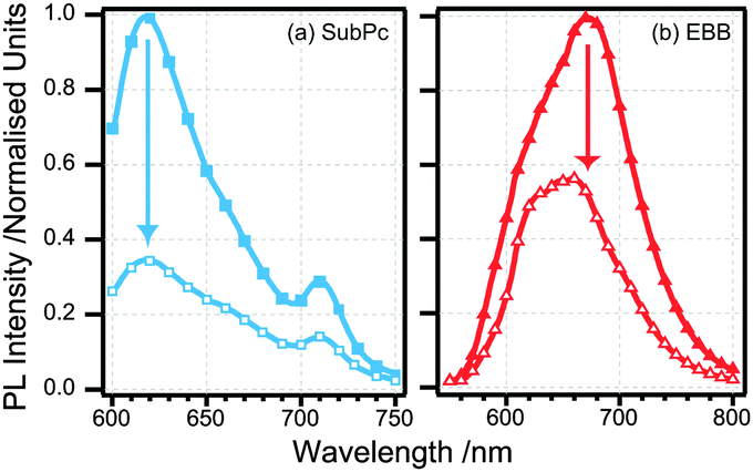 | ||
| Fig. 3 Photoluminescence spectra of (a) 25 nm SubPc film excited at 590 nm without (filled squares) and with (open squares) a 20 nm EBB quenching layer and (b) 25 nm EBB film excited at 450 nm without (filled triangles) and with (open triangles) a 20 nm SubPc quenching layer. In both cases the plots are normalised to the peak in the non-quenched spectrum. | ||
To determine electron mobility in the EBB films, electron-only devices with structure ITO/Zr(acac)/EBB (100 nm)/Al (200 nm) were fabricated and the mobility measured by the space-charge limited current (SCLC) method. Zr(acac) has recently been shown as an effective electron transport layer for a range of active materials.19 A Mott–Gurney fit to the J–V data (Fig. S1, ESI†) yields a zero-field mobility of μ0 = 1.25 × 10⁻⁷ cm2 V−1 s−1. The OPV orientation (perpendicular) electron mobility in C60 is typically reported as high as 5.1 × 10⁻² cm2 V−1 s−1;20,21 significantly higher than that of EBB. However, there is evidence that matched mobility between donor and acceptor material can be more critical than absolute mobility,22 and so with a reported hole mobility in SubPc of 4.5 × 10⁻⁸ cm2 V−1 s−1,21 the value may not provide a significant bottleneck to performance.
The precise crystallographic and morphological structure of a small molecule film can significantly impact its absorption and charge transport properties, and this can sometimes be controlled through the underlying layer or substrate.23,24 Analysis of EBB thin films deposited onto ITO and various interlayers used in this work were significantly different to EBB films deposited onto octadecylsilane (ODTS) self-assembled surfaces used in the OFET studies.12 An AFM image of an EBB (50 nm) film grown on ITO (Fig. S2, ESI†) shows features of ∼100 nm in size with a surface roughness of 13.8 nm, consistent with the surface structure observed in OFET studies. However, XRD traces (Fig. S3, ESI†) of EBB films (100 nm) grown on ITO, ITO/SubPc and ITO/Zr(acac) do not show any discernible diffraction peaks, in stark contrast to those from OFET films which showed a strong peak at 2θ = ∼6.2°. Although the ITO itself produces a series of characteristic peaks, these can be assigned across all samples and are usually not sufficiently intense to mask peaks from a subsequent layer.23 The data suggests that the highly crystalline films formed in the OFET study were driven by a favourable interaction between the EBB and ODTS treated surface, whilst in this work the rougher underlying films do not show a similar interaction and lead to significantly less crystalline, even amorphous films. The lower mobility observed with these EBB films is consistent with this lower degree of crystallinity.
The SubPc/EBB system was evaluated in OPV devices based on the regular architecture of ITO/MoOx (5 nm)/SubPc (15 nm)/EBB (20 or 40 nm)/BCP (8 nm)/Al (200 nm), with J–V curves, EQE and reflective geometry absorption profiles shown in Fig. 4, and performance parameters for all devices in Table S1 (ESI†). Measuring absorption profiles in a reflective geometry, whereby the probe beam enters the structure through the transparent electrode, reflects from the back electrode and then passes through the transparent electrode before being measured, provides a total absorption profile of a complete OPV device as it would be under operation.25 This is particularly important for OPV devices containing thin discrete layers where deviation from Beer–Lambert behaviour is likely through optical interference effects which can dominate the absorption profile. At an EBB thickness of 20 nm a short-circuit current density (JSC) of 2.34 mA cm−2, VOC of 1.38 V and fill factor (FF) of 0.4 are produced resulting in a power conversion efficiency ηp = 1.28%. This VOC is the highest reported for single junction devices to date, exceeding that of recent high VOC devices using subphthalocyanine acceptor materials.9 The fact the VOC is equal to the calculated interface gap of the system (the difference between the donor HOMO and acceptor LUMO) is unexpected as a minimum 0.3 eV loss is usual. However, although the HOMO levels are determined through UPS, LUMO levels are only estimated via optical band measurements and are thus prone to significant error.12,17 A similar result is observed with SubPc/C60 junction cells which typically show VOC values ∼1.1 V, hence the absolute change in VOC upon replacing C60 with EBB is consistent.9 The EQE of the 20 nm EBB device shows a dominant SubPc contribution to the photocurrent with only a weak contribution from the EBB at ∼400–500 nm. The reflective geometry absorption spectrum confirms that this is largely a result of poor absorption in this region as it is also dominated by the SubPc peak at ∼590 nm. To address the low absorption profile a thicker layer of EBB (40 nm) was examined. Unfortunately the increased absorbance is met with a decrease in JSC and FF, with the latter caused by a significant kink in the J–V curve. This is indicative of a charge accumulation site forming in the device, likely caused by the poor electron mobility of the EBB at these thicker layers. With the acceptor thickness therefore limited to around 20 nm an alternative strategy was investigated to enhance current generation.
 | ||
| Fig. 4 (a) J–V (b) EQE and (c) reflective geometry absorption plots for regular and inverted architecture devices. | ||
Optical interference effects in discrete layer OPVs utilising reflective back electrodes are increasingly well understood. In particular it is known that an optical field intensity node is formed at the reflective electrode interface, limiting the optical intensity, and hence absorption, close to this interface.3 In regular architecture bilayer devices the optimum acceptor layer thickness tends to be significantly greater than the optimum donor layer thickness, and this is likely due to the need to move the active interface away from this low absorption region.9 This is effective only when the electron mobility of the acceptor is sufficiently high (such as for C60), but for EBB the regular architecture devices show this to not be a viable solution. Optically transparent, charge transporting spacer layers have been used extensively in tandem OPV cells to control the positioning of sub-cells within the optical field,26,27 and have seen some use in single junction devices where increasing layer thicknesses has not been desirable.28 Replacing the BCP with an electron-transporting spacer layer would be ideal, however hole-transporting spacer layers are more developed and so we investigate an inverted architecture using an NPD:MoOx hole-transporting spacer layer.26
A series of inverted devices of structure ITO/Zr(acac)/EBB (20 nm)/SubPc (20 nm)/NPD![[thin space (1/6-em)]](https://www.rsc.org/images/entities/char_2009.gif) :MoOx (6:1, 10–50 nm)/Al (200 nm) were fabricated. By keeping the thickness of both active layers fixed at 20 nm the effect of the spacer layer could be monitored as the distance from the reflective electrode to the D/A interface changed from 30–70 nm. J–V, EQE and reflective geometry absorption plots are also shown in Fig. 4 with key parameters again in Table S1 (ESI†). The VOC of the inverted devices was in the range 1.24–1.28 V, ∼0.1 V lower than those recorded for regular architecture devices. The JSC showed a significant improvement over regular architecture devices, with 3.85 mA cm−2 obtained at a spacer layer thickness of 20 nm, then decreasing at both increasing and decreasing spacer thickness. The FF was also significantly higher (∼0.5) than regular architecture devices, resulting in an average peak power conversion efficiency of 2.39% (2.57% best pixel) with a 20 nm spacer layer which compares favourably to an optimised SubPc/C60 planar junction device (3%).9 EQE and reflective geometry absorption measurements provide an insight into the origin of this improvement in JSC. Comparing the inverted architecture device with a 20 nm spacer layer to the regular architecture device with a 20 nm EBB layer an improvement in EQE is observed across the spectrum, with an increase from 0.28 to 0.36 at the peak around 585 nm (approximately the peak absorption of SubPc) and from 0.13 to 0.27 at 480 nm (the peak absorption of EBB).
:MoOx (6:1, 10–50 nm)/Al (200 nm) were fabricated. By keeping the thickness of both active layers fixed at 20 nm the effect of the spacer layer could be monitored as the distance from the reflective electrode to the D/A interface changed from 30–70 nm. J–V, EQE and reflective geometry absorption plots are also shown in Fig. 4 with key parameters again in Table S1 (ESI†). The VOC of the inverted devices was in the range 1.24–1.28 V, ∼0.1 V lower than those recorded for regular architecture devices. The JSC showed a significant improvement over regular architecture devices, with 3.85 mA cm−2 obtained at a spacer layer thickness of 20 nm, then decreasing at both increasing and decreasing spacer thickness. The FF was also significantly higher (∼0.5) than regular architecture devices, resulting in an average peak power conversion efficiency of 2.39% (2.57% best pixel) with a 20 nm spacer layer which compares favourably to an optimised SubPc/C60 planar junction device (3%).9 EQE and reflective geometry absorption measurements provide an insight into the origin of this improvement in JSC. Comparing the inverted architecture device with a 20 nm spacer layer to the regular architecture device with a 20 nm EBB layer an improvement in EQE is observed across the spectrum, with an increase from 0.28 to 0.36 at the peak around 585 nm (approximately the peak absorption of SubPc) and from 0.13 to 0.27 at 480 nm (the peak absorption of EBB).
In summary, we have demonstrated a new type of electron acceptor material for evaporable organic photovoltaics based on an N-ethyl barbituric acid bithiophene derivative. The material, having frontier orbital energies comparable to the commonly used fullerene derivatives, was demonstrated to effectively quench excitons in both directions when combined with a SubPc donor material. Devices employing this donor–acceptor combination showed exceptionally high VOC values up to 1.38 V; amongst the highest reported for single junction devices. Despite a relatively low OPV-geometry electron mobility, inverted architecture cells employing a hole transporting optical spacer layer achieved power conversion efficiencies of almost 2.6%. Whilst modest in terms of current state of the art devices, it is worth noting that this efficiency is ∼86% of that obtained from an optimised SubPc/C60 based device, proving the potential of the these types of n-type material to compete with fullerene derivatives when used in higher performing multijunction and cascade devices.
This work was supported by the Engineering and Physical Sciences Research Council [Grant Number EP/J500057/1 and EP/H021388/1] and the Flexible Electronic Theme at CSIRO Manufacturing Flagship. The Panalytical® MRD diffractometer used in this research was obtained through the Science City Advanced Materials Project: Creating and Characterizing Next Generation Advanced Materials, with support from Advantage West Midlands (AWM) and part funded by the European Regional Development Fund (ERDF).
Notes and references
- (a) J. You, L. Dou, K. Yoshimura, T. Kato, K. Ohya, T. Moriarty, K. Emery, C.-C. Chen, J. Gao, G. Li and Y. Yang, Nat. Commun., 2013, 4, 1446 CrossRef PubMed; (b) X. Che, X. Xiao, J. D. Zimmerman, D. Fan and S. R. Forrest, Adv. Energy Mater., 2014, 4, 1400568 CrossRef; (c) Z. He, C. Zhong, S. Su, M. Xu, H. Wu and Y. Cao, Nat. Photonics, 2012, 6, 591 Search PubMed; (d) A. Mishra and P. Bäuerle, Angew. Chem., Int. Ed., 2012, 51, 2020 CrossRef CAS PubMed; (e) Y. Lin, Y. Li and X. Zhan, Chem. Soc. Rev., 2012, 41, 4245 RSC.
- A. F. Eftaiha, J.-P. Sun, I. G. Hill and G. C. Welch, J. Mater. Chem. A, 2014, 2, 1201 CAS.
- W. Cao and J. Xue, Energy Environ. Sci., 2014, 7, 2123 CAS.
- J. C. Bijleveld, R. A. M. Verstrijden, M. M. Wienk and R. A. J. Janssen, Appl. Phys. Lett., 2010, 97, 073304 CrossRef PubMed.
- (a) P. Sonar, J. P. F. Lim and K. L. Chan, Energy Environ. Sci., 2011, 4, 1558 RSC; (b) F. Zhang, D. Wu, Y. Xu and X. Feng, J. Mater. Chem., 2011, 21, 17590 RSC; (c) Y. Lin and X. Zhan, Mater. Horiz., 2014, 1, 470 RSC.
- (a) J. Zhao, Y. Li, H. Lin, Y. Liu, K. Jiang, C. Mu, T. Ma, J. Y. L. Lai, H. Hu, D. Yuc and H. Yan, Energy Environ. Sci., 2015, 8, 520 RSC; (b) Y. Lin, J. Wang, Z.-G. Zhang, H. Bai, Y. Li, D. Zhu and X. Zhan, Adv. Mater., 2015, 27, 1170 CrossRef CAS PubMed.
- C. Uhrich, R. Schueppel, A. Petrich, M. Pfeiffer, K. Leo, E. Brier, P. Kilickiran and P. Baeuerle, Adv. Funct. Mater., 2007, 17, 2991 CrossRef CAS.
- B. Verreet, B. P. Rand, D. Cheyns, A. Hadipour, T. Aernouts, P. Heremans, A. Medina, C. G. Claessens and T. Torres, Adv. Energy Mater., 2011, 1, 565 CrossRef CAS.
- P. Sullivan, A. Duraud, I. Hancox, N. Beaumont, G. Mirri, J. H. R. Tucker, R. A. Hatton, M. Shipman and T. S. Jones, Adv. Energy Mater., 2011, 1, 352 CrossRef CAS.
- K. Cnops, B. P. Rand, D. Cheyns, B. Verreet, M. A. Empl and P. Heremans, Nat. Commun., 2014, 5, 1 Search PubMed.
- (a) K. B. Burke, Y. Shu, P. Kemppinen, B. Singh, M. Bown, I. Liaw, R. M. Williamson, L. Thomsen, P. Dastoor, W. Belcher, C. Forsyth, K. N. Winzenberg and G. E. Collis, Cryst. Growth Des., 2012, 12, 725 CrossRef CAS; (b) Y. Shu, G. E. Collis, C. J. Dunn, P. Kemppinen, K. N. Winzenberg, R. M. Williamson, A. Bilic, T. B. Singh, M. Bown, C. R. McNeill and L. Thomsen, J. Mater. Chem. C, 2013, 1, 6299 RSC.
- Y. Shu, A. Mikosch, K. N. Winzenberg, P. Kemppinen, C. D. Easton, A. Bilic, C. M. Forsyth, C. J. Dunn, T. B. Singh and G. E. Collis, J. Mater. Chem. C, 2014, 2, 3895 RSC.
- K. N. Winzenberg, P. Kemppinen, G. Fanchini, M. Bown, G. E. Collis, C. M. Forsyth, K. Hegedus, T. B. Singh and S. E. Watkins, Chem. Mater., 2009, 21, 5701 CrossRef CAS.
- K. N. Winzenberg, P. Kemppinen, F. H. Scholes, G. E. Collis, Y. Shu, T. B. Singh, A. Bilic, C. M. Forsyth and S. E. Watkins, Chem. Commun., 2013, 49, 6307 RSC.
- C.-W. Chu, V. Shrotriya, G. Li and Y. Yang, Appl. Phys. Lett., 2006, 88, 153504 CrossRef PubMed.
- K. L. Mutolo, E. I. Mayo, B. P. Rand, S. R. Forrest and M. E. Thompson, J. Am. Chem. Soc., 2006, 128, 8108 CrossRef CAS PubMed.
- N. Beaumont, S. W. Cho, P. Sullivan, D. Newby, K. E. Smith and T. S. Jones, Adv. Funct. Mater., 2012, 22, 561 CrossRef CAS.
- N. Beaumont, J. S. Castrucci, P. Sullivan, G. E. Morse, A. S. Paton, Z.-H. Lu, T. P. Bender and T. S. Jones, J. Phys. Chem. C, 2014, 118, 14813 CAS.
- Z. Tan, S. Li, F. Wang, D. Qian, J. Lin, J. Hou and Y. Li, Sci. Rep., 2014, 4, 4691 Search PubMed.
- B. P. Rand, J. Xue, S. Uchida and S. R. Forrest, J. Appl. Phys., 2005, 98, 124902 CrossRef PubMed.
- R. Pandey, A. A. Gunawan, K. A. Mkhoyan and R. J. Holmes, Adv. Funct. Mater., 2012, 22, 617 CrossRef CAS.
- W. Tress, A. Petrich, M. Hummert, M. Hein, K. Leo and M. Riede, Appl. Phys. Lett., 2011, 98, 063301 CrossRef PubMed.
- P. Sullivan, T. S. Jones, A. J. Ferguson and S. Heutz, Appl. Phys. Lett., 2007, 91, 233114 CrossRef PubMed.
- (a) L. Li, W. Hiu, H. Fuchs and L. Chi, Adv. Energy Mater., 2011, 1, 188 CrossRef CAS; (b) C. Schünemann, D. Wynands, K.-J. Eichhorn, M. Stamm, K. Leo and M. Riede, J. Phys. Chem. C, 2013, 117, 11600 CrossRef.
- G. F. Burkhard, E. T. Hoke and M. D. McGehee, Adv. Mater., 2010, 22, 3293 CrossRef CAS PubMed.
- E. New, T. Howells, P. Sullivan and T. S. Jones, Org. Electron., 2013, 14, 2353 CrossRef CAS PubMed.
- R. Schueppel, R. Timmreck, N. Allinger, T. Mueller, M. Furno, C. Uhrich, K. Leo and M. Riede, J. Appl. Phys., 2010, 107, 044503 CrossRef PubMed.
- R. Fitzner, E. Reinold, A. Mishra, E. Mena-Osteritz, H. Ziehlke, C. Körner, K. Leo, M. Riede, M. Weil, O. Tsaryova, A. Weiß, C. Uhrich, M. Pfeiffer and P. Bäuerle, Adv. Funct. Mater., 2011, 21, 897 CrossRef CAS.
Footnote |
| † Electronic supplementary information (ESI) available: Contains information on materials, film characterisation, device fabrication, UV/Visible, photoluminescence, electron mobility, AFM, XRD and OPV device data. See DOI: 10.1039/c5cc00564g |
| This journal is © The Royal Society of Chemistry 2015 |