
 Open Access Article
 This Open Access Article is licensed under a Creative Commons Attribution-Non Commercial 3.0 Unported Licence
Patterning of polymer brushes made easy using titanium dioxide: direct and remote photocatalytic lithography†
G.
Panzarasa‡
*a,
G.
Soliveri‡
*bc,
K.
Sparnacci
a and
S.
Ardizzone
bc
aDipartimento di Scienze e Innovazione Tecnologica, Università del Piemonte Orientale “Amedeo Avogadro”, Viale T. Michel 11, 15100 Alessandria, Italy. E-mail: guido.panzarasa@unipmn.it
bDipartimento di Chimica, Università degli Studi di Milano, Via Golgi 19, 20133 Milano, Italy. E-mail: guido.soliveri@unimi.it
cConsorzio Interuniversitario Nazionale per la Scienza e Tecnologia dei Materiali (INSTM), Via Giusti 9, 50121 Firenze, Italy
First published on 24th March 2015
Abstract
Photocatalytic lithography is proved for the realization of micropatterned polymer brushes. Initiator-functionalized titanium dioxide or silicon surfaces are respectively exposed directly to near-UV light through a photomask (direct approach) or through a transparent photoactive TiO2 film (remote approach). Initiator patterns are then amplified as polymer brushes with SI-ATRP. Features down to 10 μm could be obtained using simple equipment. The process is intrinsically parallel, has high throughput and scalable to wafer size, making it powerful for microfabrication purposes.
Polymer brushes are surface-tethered, highly-stretched polymer chains. They exhibit excellent robustness and well-organized chain conformation, which endow superior control over several surface properties such as morphology, grafting density and chemical composition.1–3 Patterned polymer brushes4,5 are versatile building blocks for micro-fabrication and controlled assembly of small particles,6 sensors/biosensors and actuators,7–15 drug delivery systems,16 electronic devices,17 anti-biofouling coatings,18 and biocompatible scaffolds.19 In general they are efficient means to confer smart, stimuli-responsive behavior to surfaces and interphases.20–22
By a combination of lithographic tools and surface-initiated polymerization (“grafting-from”, as opposed to “grafting to”, which relies on the adsorption of the preformed polymer),23,24 micro- and nanoscale-complex architectures can be readily built from suitable self-assembled monolayers (SAMs).25–28 SAMs are ordered arrays of molecules chemisorbed at a surface.29 If they are composed by polymerization initiators, chains can grow directly from them. Eventually, if the SAMs are patterned, patterned polymer brushes will be obtained.
The expertise to master the patterning30 is crucial in order to realize devices with applications ranging from biotechnology31 to electronics.32 Patterning has been accomplished using colloidal lithography,33,34 micro-contact printing,35,36 electron beam lithography,37 scanning probe38 or near field lithography,39 conventional photolithography (with the use of photoresists40,41) and SAM photolithography.42,43 The latter typically requires high-intensity UV sources6,44–46 (e.g. deep-UV and vacuum-UV)47,48 or highly focused beams (UV-lasers).49
There is a significant demand for more affordable and facile lithographic techniques, which should update the present technologies50 to reliably pattern polymer brushes at the wafer scale51 with high resolution micrometric and sub-micrometric features. Here, for the first time, we describe how this challenge can be successfully addressed by taking advantage of titanium dioxide photocatalytic properties. To date, this technique has been used mostly to build hydrophilic/hydrophobic patterns.52,53
TiO2 is one of the major protagonists in nanotechnology. It is inexpensive and non-toxic; its surface is biocompatible and can be functionalized using established chemistries.54 The oxide is an intrinsic semiconductor whose photochemical and photophysical properties have had great relevance both in fundamental55,56 and applied57,58 research. When TiO2 is irradiated with photons of wavelength in the UV region, electron–hole pairs are produced: holes are powerful oxidants, electrons are good reducing agents and both rapidly react with adsorbates.59 Titanium dioxide is now playing a central role in the engineering of surfaces,60,61 in particular in the field of lithography.53,62 Here, we report for the first time improved access to micro-patterned polymer brushes using near-UV light titanium dioxide photocatalytic lithography.
Photocatalytic lithography was presently performed on lab-made substrates. We deposited transparent and mechanically robust TiO2 anatase films with high photoactivity on glass and silicon wafer (Fig. S3, ESI†) from an acidic TiO2 sol using the electrochemically-assisted technique, first reported by our group.63 The requirement of common lab instrumentation and the possibility to store and reuse the sol for up to one month have made this process highly appealing, cheap and scalable. In addition, the quality of the TiO2 film is comparably better in terms of smoothness (rms 0.563 nm) compared to those commonly obtained by dip-coating or spin-coating.64 Film thickness can be increased at will by repeating the deposition cycle.63 Films showed the typical increase in hydrophilicity upon exposure to 365 nm UV radiation due to enhanced hydroxyl surface termination (generally reported as “surface-induced hydrophilicity”65). We exploited this phenomenon to improve chemisorption of the atom transfer radical polymerization (ATRP) initiator (3-(2-bromoisobutyramido)propyl)triethoxysilane (BIB-APTES)66 on TiO2 (Fig. 1, step 1). Direct photocatalytic micropatterning of the initiator was achieved through UV-irradiation with 365 nm UV light from a halogen lamp using a TEM grid on the substrate as a photomask (Fig. 1, step 2a).
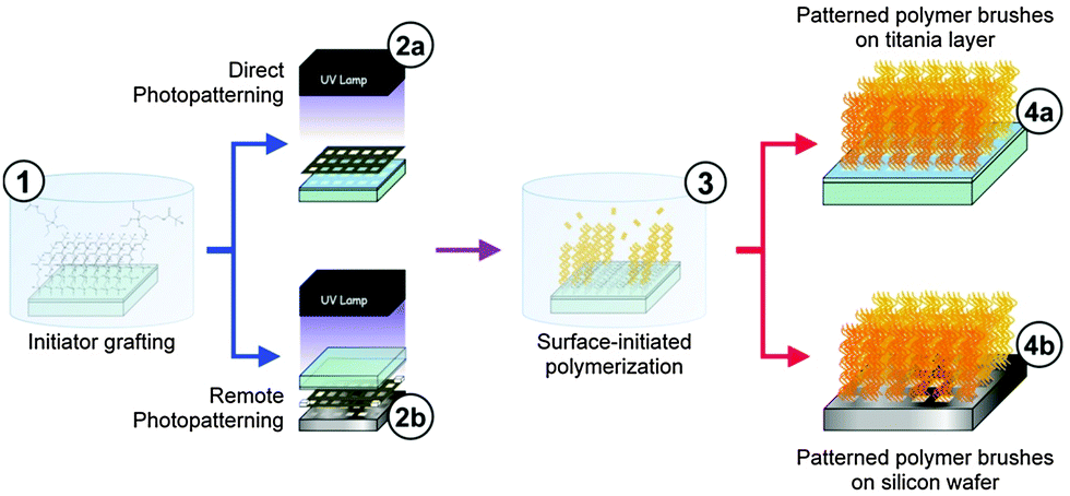 | ||
| Fig. 1 Preparation of patterned brushes. Grafting of the ATRP initiator (1), pattern formation using both direct (2a) and remote (2b) photocatalytic lithography, SI-ATRP (3) and the obtained polymer patterns (4a, 4b). | ||
Photocatalytic degradation could be easily followed on dedicated substrates by water contact angle measurements (Fig. S4, ESI†). The water contact angle for surfaces functionalized with BIB-APTES, stored in the dark, was 75°. After 1 h of irradiation, the θw decreased to less than 15° and the disappearance of nitrogen and bromine signals from the XPS spectra gave definitive evidence of complete deactivation of the initiator molecules (Table S1, ESI†). On the other hand, BIB-APTES grafted on surfaces with no photoactivity, like silicon wafer or glass, was unaffected even after more than 5 h of UV irradiation as confirmed by the unchanged water contact angle and the ability to start the growth of polymer brushes. This confirmed the critical role of TiO2 in the photo-patterning of the initiator; a 365 nm lamp (working at 60 mW power density) does not allow photolysis of the adsorbates.
We used surface-initiated atom transfer radical polymerization (SI-ATRP), a controlled free radical polymerization process, to amplify the obtained initiator pattern into a poly(methyl methacrylate) (PMMA) brush.67,68 As a proof of concept, we chose the methyl methacrylate (MMA) monomer but, in principle, any ATRP-friendly monomer can be used. Activators regenerated by electron transfer (ARGET) ATRP was selected because, in contrast to classical ATRP, offers improved oxygen tolerance and permits the adoption of milder conditions.69 PMMA brush growth was carried out at 30 °C in a 4![[thin space (1/6-em)]](https://www.rsc.org/images/entities/char_2009.gif) :1 v/v methanol–water mixture using a CuBr2/tris(2-pyridylmethyl)amine (TPMA) catalyst activated by an excess of ascorbic acid. Polymerization of BIB-APTES-functionalized substrates proceeded smoothly, leading to PMMA brushes with thicknesses up to 200 nm depending upon the amount of time allowed for polymerization (Fig. S5, ESI†). Successful grafting of polymer brushes was confirmed by water contact angle measurements (68°, which is consistent with previous wetting experiments with water on PMMA brushes70) and FTIR analysis (Fig. S6b, ESI†). The brush thickness is linearly correlated with polymerization time (over at least 8 h) suggesting a good control of the polymerization (Fig. S5, ESI†). Fig. 2 shows that the grid patterns have been successfully replicated onto the TiO2 surface and 10 μm-wide PMMA lines were obtained with very good resolution (see also Fig. S7, ESI†). Remarkably, the brushes were able to restart the polymerization of MMA with excellent (≥90%) reinitiation efficiency (Fig. S6a, ESI†) and also allowed the formation of block-copolymers: for example PMMA-b-PS brushes, with a PS block up to 80 nm thick, could be obtained by subsequent polymerization of styrene on a PMMA brush as shown by the increase in the contact angle (from 68° to 90°, in accordance with literature findings71) and FTIR analysis (Fig. S6b and c, ESI†).
:1 v/v methanol–water mixture using a CuBr2/tris(2-pyridylmethyl)amine (TPMA) catalyst activated by an excess of ascorbic acid. Polymerization of BIB-APTES-functionalized substrates proceeded smoothly, leading to PMMA brushes with thicknesses up to 200 nm depending upon the amount of time allowed for polymerization (Fig. S5, ESI†). Successful grafting of polymer brushes was confirmed by water contact angle measurements (68°, which is consistent with previous wetting experiments with water on PMMA brushes70) and FTIR analysis (Fig. S6b, ESI†). The brush thickness is linearly correlated with polymerization time (over at least 8 h) suggesting a good control of the polymerization (Fig. S5, ESI†). Fig. 2 shows that the grid patterns have been successfully replicated onto the TiO2 surface and 10 μm-wide PMMA lines were obtained with very good resolution (see also Fig. S7, ESI†). Remarkably, the brushes were able to restart the polymerization of MMA with excellent (≥90%) reinitiation efficiency (Fig. S6a, ESI†) and also allowed the formation of block-copolymers: for example PMMA-b-PS brushes, with a PS block up to 80 nm thick, could be obtained by subsequent polymerization of styrene on a PMMA brush as shown by the increase in the contact angle (from 68° to 90°, in accordance with literature findings71) and FTIR analysis (Fig. S6b and c, ESI†).
 | ||
| Fig. 2 Direct photocatalytic lithography of the initiator and subsequent SI-ATRP. Optical microscopy (a, inset: picture of the typical sample), scanning electron microscopy (b, c) and atomic force microscopy (tapping mode, d, e and f) of the patterned surface. | ||
Direct photocatalytic lithography could play a crucial role for innovation in the field of polymer brush micro-lithography. Nevertheless, the need of a TiO2 layer or, in general, of a photoactive substrate is limiting for many applications. Notwithstanding the smoothness, the transparency, the hardness and the biocompatibility of the titania layer, its photocatalytic properties could not be desired for some applications. The necessity to graft brushes directly onto a specific surface or onto substrates that cannot withstand thermal treatments (needed for the development of titania photoactivity) could occur. We found in remote photocatalysis a powerful solution for this general problem. The group of Fujishima, first, reported that the photooxidation of organic molecules can take place not only on the direct titanium dioxide surface but also on substrates placed at relatively considerable distances (up to 500 μm) from it.65,72 The mechanism of remote photocatalysis had been highly controversial until Kubo et al.73 demonstrated that H2O2 molecules, which are generated at the photocatalyst surface from atmospheric water and oxygen, migrate in the surrounding air and are cleaved to HO˙ radicals in the exposed areas of the target surface. Such a mechanism is particularly useful to explain the high resolution pattern obtained. Highly oxidative radical species form only in the irradiated areas, avoiding lateral oxidation due to migration.74,75 Remote oxidation of organic contaminants, alkylsiloxane and thiol SAMs, polymers and metals has been reported,76,77 especially oriented to the generation of superhydrophilic/superhydrophobic patterns.75 Here, for the first time, we describe the successful application of remote photocatalytic lithography for the realization of patterned polymer brushes. This is potentially a universal approach, able to generate high resolution patterns on any kind of substrate. In order to obtain a good resolution, avoiding effects connected to the titania substrate morphology and light scattering ability, the quality of the photoactive layer is critical. Again, electrochemically-assisted titania deposition gave high performance in terms of transparency and smoothness (Fig. S3, ESI†). Remote photocatalytic patterning was performed by irradiating with 365 nm UV light BIB-APTES-functionalized silicon substrates through our titania-coated glass, pre-cleaned by UV irradiation for 1 h, using a 100 μm-thick Teflon spacer (Fig. 1, step 2b). Micropatterning was achieved using a TEM grid and patterns were amplified with PMMA brushes, as already discussed for direct photolithography. The water contact angle decreased from 70° to 33° after 2 h irradiation of the initiator-functionalized substrate. In addition, as for the direct approach, XPS showed complete disappearance of the bromine signal (Table S1, ESI†). Nevertheless, the best pattern resolution was achieved with an irradiation time of 5 h. A complete optical and electron microscopic characterization is shown in Fig. 3 and Fig. S8, ESI†.
 | ||
| Fig. 3 Remote photocatalytic lithography of the initiator and subsequent SI-ATRP. Optical microscopy (a, b), scanning electron microscopy (c) of the patterned silica substrate. | ||
To conclude, the growing excitement in the field of polymer brushes and the proved request for efficient patterning means urge the introduction of more facile and low-cost method to develop such architectures. Here, we discussed for the first time the use of photocatalytic lithography for making patterned polymer brushes, showing how innovative this approach could be. Titanium dioxide high photoactivity was employed to selectively degrade initiators of polymerization under near-UV irradiation through a photomask, and the obtained patterns were replicated by SI-ATRP. While direct photocatalytic lithography could be obtained only on the surface of a thin titania layer, the remote approach allowed us to achieve photocatalytic patterning on, virtually, any kind of substrate thanks to the migration of oxidizing species from a TiO2 interface. Both approaches lead to sharp edges and high line resolution. The remote approach is especially relevant being a general, non-invasive and high-throughput lithographic technique. We deliberately chose cheap materials (e.g. glass instead of quartz slides) to make it affordable to a wider spectrum of researchers. Long time irradiation was correlated with a low-energetic lithographic lamp (safe and simple to handle); in such a way, high resolution is simple to reach. In addition, our process can be scaled up to the wafer scale, with the future final goal to design controlled areas with different functionalities, useful for applications, e.g. in microfluidics and for the development of cell-responsive surfaces.
The authors want to express their gratitude to Dr L. Meda and Dr G. Marra (Research Center for Non-Conventional Energies, ENI Donegani Institute, Novara) for kindly providing the X-ray photoelectron spectroscopy (XPS) analyses, the scanning electron microscopy (SEM) images and X-ray diffraction (XRD) analyses, respectively. G.S. would like to thank Dr S. Hoeppener.
Notes and references
- R. Barbey, L. Lavanant, D. Paripovic, N. Schüwer, C. Sugnaux, S. Tugulu and H.-A. Klok, Chem. Rev., 2009, 109, 5437–5527 CrossRef CAS PubMed.
- S. G. Boyes, A. M. Granville, M. Baum, B. Akgun, B. K. Mirous and W. J. Brittain, Surf. Sci., 2004, 570, 1–12 CrossRef CAS PubMed.
- O. Azzaroni, J. Polym. Sci., Part A: Polym. Chem., 2012, 50, 3225–3258 CrossRef CAS.
- T. Chen, I. Amin and R. Jordan, Chem. Soc. Rev., 2012, 41, 3280–3296 RSC.
- M. E. Welch and C. K. Ober, J. Polym. Sci., Part B: Polym. Phys., 2013, 51, 1457–1472 CrossRef.
- G. J. Dunderdale, J. R. Howse and J. P. A. Fairclough, Langmuir, 2011, 27, 11801–11805 CrossRef CAS PubMed.
- J. Cui, O. Azzaroni and A. del Campo, Macromol. Rapid Commun., 2011, 32, 1699–1703 CrossRef CAS PubMed.
- G. J. Dunderdale and J. P. A. Fairclough, Langmuir, 2013, 29, 3628–3635 CrossRef CAS PubMed.
- M. Singh, O. Odusanya, G. M. Wilmes, H. B. Eitouni, E. D. Gomez, A. J. Patel, V. L. Chen, M. J. Park, P. Fragouli, H. Iatrou, N. Hadjichristidis, D. Cookson and N. P. Balsara, Macromolecules, 2007, 40, 4578–4585 CrossRef CAS.
- C. R. Daniels, L. J. Tauzin, E. Foster, R. C. Advincula and C. F. Landes, J. Phys. Chem. B, 2013, 117, 4284–4290 CrossRef CAS PubMed.
- I. Tokareva, I. Tokarev, S. Minko, E. Hutter and J. H. Fendler, Chem. Commun., 2006, 3343–3345 RSC.
- T. Chen, R. Ferris, J. Zhang, R. Ducker and S. Zauscher, Prog. Polym. Sci., 2010, 35, 94–112 CrossRef CAS PubMed.
- H. Ma, J. He, X. Liu, J. Gan, G. Jin and J. Zhou, ACS Appl. Mater. Interfaces, 2010, 2, 3223–3230 CAS.
- H. C. McCaig, E. Myers, N. S. Lewis and M. L. Roukes, Nano Lett., 2014, 14, 3728–3732 CrossRef CAS PubMed.
- C. Xu, X. Fu, M. Fryd, S. Xu, B. B. Wayland, K. I. Winey and R. J. Composto, Nano Lett., 2006, 6, 282–287 CrossRef CAS PubMed.
- S. Kumar, Y. L. Dory, M. Lepage and Y. Zhao, Macromolecules, 2011, 44, 7385–7393 CrossRef CAS.
- H. J. Snaith, G. L. Whiting, B. Sun, N. C. Greenham, W. T. S. Huck and R. H. Friend, Nano Lett., 2005, 5, 1653–1657 CrossRef CAS PubMed.
- G. Gunkel, M. Weinhart, T. Becherer, R. Haag and W. T. S. Huck, Biomacromolecules, 2011, 12, 4169–4172 CrossRef CAS PubMed.
- D. Falconnet, G. Csucs, H. M. Grandin and M. Textor, Biomaterials, 2006, 27, 3044–3063 CrossRef CAS PubMed.
- S. Peng and B. Bhushan, RSC Adv., 2012, 2, 8557 RSC.
- F. Zhou and W. T. S. Huck, Phys. Chem. Chem. Phys., 2006, 8, 3815 RSC.
- S. Dai, P. Ravi and K. C. Tam, Soft Matter, 2008, 4, 435 RSC.
- A. Olivier, F. Meyer, J. Raquez, P. Damman and P. Dubois, Prog. Polym. Sci., 2012, 37, 157–181 CrossRef CAS PubMed.
- D. M. Jones and W. T. S. Huck, Adv. Mater., 2001, 13, 1256 CrossRef CAS.
- S. Santer, A. Kopyshev, H. Yang and J. Rühe, Macromolecules, 2006, 39, 3056–3064 CrossRef CAS.
- O. a. Guskova and C. Seidel, Macromolecules, 2011, 44, 671–682 CrossRef CAS.
- S. Santer, A. Kopyshev, J. Donges, J. Rühe, X. Jiang, B. Zhao and M. Müller, Langmuir, 2007, 23, 279–285 CrossRef CAS PubMed.
- Y.-K. Lai, Z. Chen and C.-J. Lin, J. Nanoeng. Nanomanuf., 2011, 1, 18–34 CrossRef CAS PubMed.
- A. Ulman, Chem. Rev., 1996, 96, 1533–1554 CrossRef CAS PubMed.
- M. Geissler and Y. Xia, Adv. Mater., 2004, 16, 1249–1269 CrossRef CAS.
- Q. Liu, C. Wu, H. Cai, N. Hu, J. Zhou and P. Wang, Chem. Rev., 2014, 114, 6423–6461 CrossRef CAS PubMed.
- E. Menard, M. A. Meitl, Y. Sun, J. Park, D. J. Shir, Y. Nam, S. Jeon and J. A. Rogers, Chem. Rev., 2007, 107, 1117–1160 CrossRef CAS PubMed.
- Y. Li, J. Zhang, L. Fang, L. Jiang, W. Liu, T. Wang, L. Cui, H. Sun and B. Yang, J. Mater. Chem., 2012, 22, 25116 RSC.
- T. Chen, D. P. Chang, R. Jordan and S. Zauscher, Beilstein J. Nanotechnol., 2012, 3, 397–403 CrossRef PubMed.
- T. Chen, R. Jordan and S. Zauscher, Polymer, 2011, 52, 2461–2467 CrossRef CAS PubMed.
- Y. Tsujii, M. Ejaz, S. Yamamoto, T. Fukuda, K. Shigeto, K. Mibu and T. Shinjo, Polymer, 2002, 43, 3837–3841 CrossRef CAS.
- S. J. Ahn, M. Kaholek, W.-K. Lee, B. LaMattina, T. H. LaBean and S. Zauscher, Adv. Mater., 2004, 16, 2141–2145 CrossRef CAS.
- M. Kaholek, W. Lee, B. LaMattina, K. C. Caster and S. Zauscher, Nano Lett., 2004, 4, 373–376 CrossRef CAS.
- E. ul Haq, Z. Liu, Y. Zhang, S. a. A. Ahmad, L.-S. Wong, S. P. Armes, J. K. Hobbs, G. J. Leggett, J. Micklefield, C. J. Roberts and J. M. R. Weaver, Nano Lett., 2010, 10, 4375–4380 CrossRef CAS PubMed.
- X. Fan, L. Lin, J. L. Dalsin and P. B. Messersmith, Polym. Prepr., 2005, 46, 442–443 CAS.
- J.-K. Chen, Z.-Y. Chen, H.-C. Lin, P.-D. Hong and F.-C. Chang, ACS Appl. Mater. Interfaces, 2009, 1, 1525–1532 CAS.
- N. Herzer, S. Hoeppener and U. S. Schubert, Chem. Commun., 2010, 46, 5634–5652 RSC.
- S. Hoeppener, R. Maoz and J. Sagiv, Nano Lett., 2003, 3, 761–767 CrossRef CAS.
- S. A. Ahmad, G. J. Leggett, A. Hucknall and A. Chilkoti, Biointerphases, 2011, 6, 8–15 CrossRef PubMed.
- R. Iwata, P. Suk-In, V. P. Hoven, A. Takahara, K. Akiyoshi and Y. Iwasaki, Biomacromolecules, 2004, 5, 2308–2314 CrossRef CAS PubMed.
- S. Tugulu, M. Harms, M. Fricke, D. Volkmer and H.-A. Klok, Angew. Chem., Int. Ed., 2006, 45, 7458–7461 CrossRef CAS PubMed.
- O. P. Khatri, H. Sano, K. Murase and H. Sugimura, Langmuir, 2008, 24, 12077–12084 CrossRef CAS PubMed.
- M. Yamaguchi, K. Ikeda, M. Suzuki, A. Kiyohara, S. N. Kudoh, K. Shimizu, T. Taira, D. Ito, T. Uchida and K. Gohara, Langmuir, 2011, 27, 12521–12532 CrossRef CAS PubMed.
- S. Sun and G. J. Leggett, Nano Lett., 2007, 7, 3753–3758 CrossRef CAS.
- S. Nishimoto, A. Kubo, K. Nohara, X. Zhang, N. Taneichi, T. Okui, Z. Liu, K. Nakata, H. Sakai, T. Murakami, M. Abe, T. Komine and A. Fujishima, Appl. Surf. Sci., 2009, 255, 6221–6225 CrossRef CAS PubMed.
- Z. Xie, C. Chen, X. Zhou, T. Gao, D. Liu, Q. Miao and Z. Zheng, ACS Appl. Mater. Interfaces, 2014, 6, 11955–11964 CAS.
- K. Nakata and A. Fujishima, J. Photochem. Photobiol., C, 2012, 13, 169–189 CrossRef CAS PubMed.
- K. Liu, M. Cao, A. Fujishima and L. Jiang, Chem. Rev., 2014, 114, 10044–10094 CrossRef CAS PubMed.
- H. Park, Y. Park, W. Kim and W. Choi, J. Photochem. Photobiol., C, 2013, 15, 1–20 CrossRef CAS PubMed.
- U. Diebold, Surf. Sci. Rep., 2003, 48, 53–229 CrossRef CAS.
- C. Marchiori, G. Di Liberto, G. Soliveri, L. Loconte, L. Lo Presti, D. Meroni, M. Ceotto, C. Oliva, S. Cappelli, G. Cappelletti, C. Aieta and S. Ardizzone, J. Phys. Chem. C, 2014, 118, 24152–24164 CAS.
- K. Nakata, T. Ochiai, T. Murakami and A. Fujishima, Electrochim. Acta, 2012, 84, 103–111 CrossRef CAS PubMed.
- A. Antonello, G. Soliveri, D. Meroni, G. Cappelletti and S. Ardizzone, Catal. Today, 2014, 230, 35–40 CrossRef CAS PubMed.
- O. Carp, Prog. Solid State Chem., 2004, 32, 33–177 CrossRef CAS PubMed.
- G. Soliveri, R. Annunziata, S. Ardizzone, G. Cappelletti and D. Meroni, J. Phys. Chem. C, 2012, 116, 26405–26413 CAS.
- G. Soliveri, D. Meroni, G. Cappelletti, R. Annunziata, V. Aina, G. Cerrato and S. Ardizzone, J. Mater. Sci., 2014, 49, 2734–2744 CrossRef CAS.
- Y. Paz, Beilstein J. Nanotechnol., 2011, 2, 845–861 CrossRef CAS PubMed.
- G. Maino, D. Meroni, V. Pifferi, L. Falciola, G. Soliveri, G. Cappelletti and S. Ardizzone, J. Nanopart. Res., 2013, 15, 2087 CrossRef.
- Q. Xu, D. V. Wellia, M. A. Sk, K. H. Lim, J. S. C. Loo, D. W. Liao, R. Amal and T. T. Y. Tan, J. Photochem. Photobiol., A, 2010, 210, 181–187 CrossRef CAS PubMed.
- A. Fujishima, X. Zhang and D. Tryk, Surf. Sci. Rep., 2008, 63, 515–582 CrossRef CAS PubMed.
- X. He, W. Yang and X. Pei, Macromolecules, 2008, 41, 4615–4621 CrossRef CAS.
- K. Matyjaszewski, P. J. Miller, N. Shukla, B. Immaraporn, A. Gelman, B. B. Luokala, T. M. Siclovan, G. Kickelbick, T. Vallant, H. Hoffmann and T. Pakula, Macromolecules, 1999, 32, 8716–8724 CrossRef CAS.
- S. Edmondson, V. L. Osborne and W. T. S. Huck, Chem. Soc. Rev., 2004, 33, 14–22 RSC.
- K. Matyjaszewski, H. Dong, W. Jakubowski, J. Pietrasik and A. Kusumo, Langmuir, 2007, 23, 4528–4531 CrossRef CAS PubMed.
- Y. Ma, X. Cao, X. Feng, Y. Ma and H. Zou, Polymer, 2007, 48, 7455–7460 CrossRef CAS PubMed.
- A. Samadi, S. M. Husson, Y. Liu, I. Luzinov and S. Michael Kilbey, Macromol. Rapid Commun., 2005, 26, 1829–1834 CrossRef CAS.
- T. Tatsuma, S. Tachibana, T. Miwa, D. A. Tryk and A. Fujishima, J. Phys. Chem. B, 1999, 103, 8033–8035 CrossRef CAS.
- W. Kubo and T. Tatsuma, J. Am. Chem. Soc., 2006, 128, 16034–16035 CrossRef CAS PubMed.
- T. Tatsuma, W. Kubo and A. Fujishima, Langmuir, 2002, 18, 9632–9634 CrossRef CAS.
- N. Blondiaux, S. Zürcher, M. Liley and N. D. Spencer, Langmuir, 2007, 23, 3489–3494 CrossRef CAS PubMed.
- T. Tatsuma, S. Tachibana and A. Fujishima, J. Phys. Chem. B, 2001, 105, 6987–6992 CrossRef CAS.
- W. Kubo, T. Tatsuma, A. Fujishima and H. Kobayashi, J. Phys. Chem. B, 2004, 108, 3005–3009 CrossRef CAS.
Footnotes |
| † Electronic supplementary information (ESI) available. See DOI: 10.1039/c5cc00255a |
| ‡ These authors contributed equally. |
| This journal is © The Royal Society of Chemistry 2015 |