
 Open Access Article
 This Open Access Article is licensed under a
 Creative Commons Attribution 3.0 Unported Licence
Epitaxial growth of few-layer MoS2(0001) on FeS2{100}†
T.
Liu
,
I.
Temprano
,
D. A.
King
,
S. M.
Driver
* and
S. J.
Jenkins
Department of Chemistry, University of Cambridge, Lensfield Road, Cambridge, CB2 1EW, UK. E-mail: smd37@cam.ac.uk; Fax: +44 (0)1223 336362; Tel: +44 (0)1223 336503
First published on 13th November 2014
Abstract
Physical vapour deposition of Mo on an FeS2{100} surface was performed at 170 K. Near-epitaxial growth of MoS2(0001) overlayers of the order of 1 nm thickness was observed when the Mo-covered substrate was subsequently heated to 600 K.
Graphene is currently the most widely studied two-dimensional material due in particular to its remarkable electronic properties. However, pristine graphene has the disadvantage that it lacks a bandgap, a property that is essential for many electronic applications.1 Among alternative 2D materials, single-layer MoS2 has arisen as a promising candidate as it has an intrinsic direct bandgap of 1.8 eV (cf. an indirect gap of 1.2 eV in bulk MoS2) and thermal stability up to 1100 °C.2 MoS2 is also widely used in industry for its tribological properties (e.g. as a lubricant) and catalytic properties (e.g. in hydrodesulphurisation).3 Recent studies have indeed demonstrated the potential of 2D MoS2 in device applications such as field effect transistors,4 optoelectronics,5 spintronics and ‘valleytronics’,6 and piezotronics.7
To exploit 2D materials for device applications, it is important to develop methods of preparing large-area, well ordered layers. Bottom-up synthesis methods based on chemical vapour deposition (CVD) or self-assembled monolayers have already shown promise in delivering high quality graphene.8 Few-layer MoS2 is most commonly obtained by top-down methods such as lithium intercalation, micro mechanical exfoliation, or liquid-phase exfoliation.2 Attempts to grow high-quality MoS2 layers via CVD on different surfaces have yielded mixed results so far. For example, large area MoS2 atomic layers have been produced on insulating surfaces (sapphire and SiO2) and on graphene,9 whereas MoS2 nanoclusters were found to form when Mo was deposited on Au{111} or HOPG under a pressure of H2S.10
Here, we describe facile bottom-up epitaxial growth of a highly ordered MoS2(0001) film, of the order of 1 nm thick, on a semiconducting substrate: this has not, to our knowledge, been reported before. It was achieved by physical vapour deposition (PVD) under ultra-high vacuum (UHV) on {100} surfaces of FeS2 (iron pyrite). FeS2 is of considerable interest in its own right for its electronic and optical properties, in view of its natural abundance. Moreover, the epitaxy points strongly to FeS2/MoS2 interface structure that is crystallographically well defined: this is likely to be beneficial for device applications in terms of its electronic properties and charge transport behaviour.11
Our experiments were performed under UHV (base pressure ∼1 × 10⁻¹⁰ mbar) in an apparatus described elsewhere.12 As-grown {100} surfaces of naturally occurring FeS2 crystals (Manchester Minerals) were used as substrates; these were prepared as described previously to obtain a highly-ordered stoichiometric termination.12 The maximum temperature was kept below 630 K to avoid decomposition of the pyrite crystal. Mo was deposited by evaporation from a Mo rod (Goodfellow, 1.0 mm diameter, 99.99% purity), electron beam heated within an evaporator (Omicron EFM3) operated at 910 eV and 40 mA emission.
Stepwise deposition of Mo (with the substrate held at 170 K during deposition, followed by a flash anneal to 600 K after each deposition step) on pristine FeS2{100} was monitored by Auger electron spectroscopy (AES). Mo/S and Fe/S Auger peak height ratios are displayed in Fig. 1 as a function of Mo deposition time. The cumulative deposition of Mo is reflected in a linear increase of the Mo/S ratio. The Fe/S ratio, by contrast, decreased quickly and linearly up to 9 min Mo deposition. Thereafter, the Fe/S ratio remained approximately constant at less than 10% of its initial value. At this point the Fe50 Auger signal of the FeS2{100} substrate is almost totally blocked by the deposited layer. This, in turn, implies that the outermost surface region has been transformed from iron sulphide to a layer of molybdenum sulphide. It is important to note that no S was introduced from external sources in this work. The only S available to react with the deposited metallic Mo layer must therefore have come from the pyrite crystal. Thermal diffusion of S from the bulk has been previously reported to cause recovery of the stoichiometry on S-depleted FeS2{100} surfaces.12
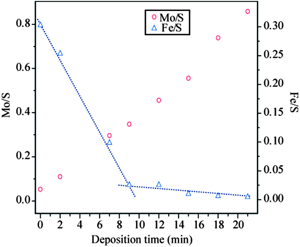 | ||
| Fig. 1 Mo/S and Fe/S Auger peak height ratios (measured for the Mo peak at 190 eV kinetic energy, the Fe peak at 50 eV and the S peak at 155 eV) as a function of Mo deposition time on FeS2{100} surface (substrate was flash-annealed to 600 K between successive deposition steps). | ||
The structural characteristics of the molybdenum sulphide overlayer were monitored by means of low energy electron diffraction (LEED). For the clean surface prior to Mo deposition, a diffraction pattern with a square array of sharp spots is observed, consistent with the (1 × 1) lattice of bulk-terminated FeS2{100}. The spot sharpness was routinely monitored and provides a qualitative indication of the surface order of the substrate prior to and after exposure to Mo. Fig. 2a shows the diffraction pattern of the surface after 2 min Mo deposition, corresponding to a Mo/S AES peak height ratio of 0.11: the pattern is unchanged from that of the clean surface. An increase in the deposition time to a total of 7 min (Mo/S = 0.29), however, leads to the emergence of an additional hexagonal pattern, with a well-defined orientation relative to the coexisting square pattern of the substrate (Fig. 2b). At this relatively low Mo coverage the hexagonal pattern appears as low intensity, though quite sharp, spots whereas the square lattice spots remain sharp and intense. We ascribe the hexagonal pattern to the growth of regions of MoS2(0001). From the bulk lattice parameters of FeS2 (a = 5.416 Å)13 and MoS2 (a = 3.16 Å),14 as marked on the ball models of their structures in Fig. 3, it follows that the surface reciprocal lattice vectors have values a1* = a2* = 2.30 Å−1 for MoS2(0001) and b1* = b2* = 1.16 Å−1 for FeS2{100}, i.e. a1* is within 1% of 2b1*. Accordingly, certain spots of the hexagonal and square LEED patterns will coincide if the two lattices have the correct relative mutual orientation. The reciprocal vectors marked on the LEED pattern in Fig. 2b show that a2* is indeed coincident with 2b1*. There is evidently a well-defined epitaxial relationship between the two real-space structures, which we discuss in detail below.
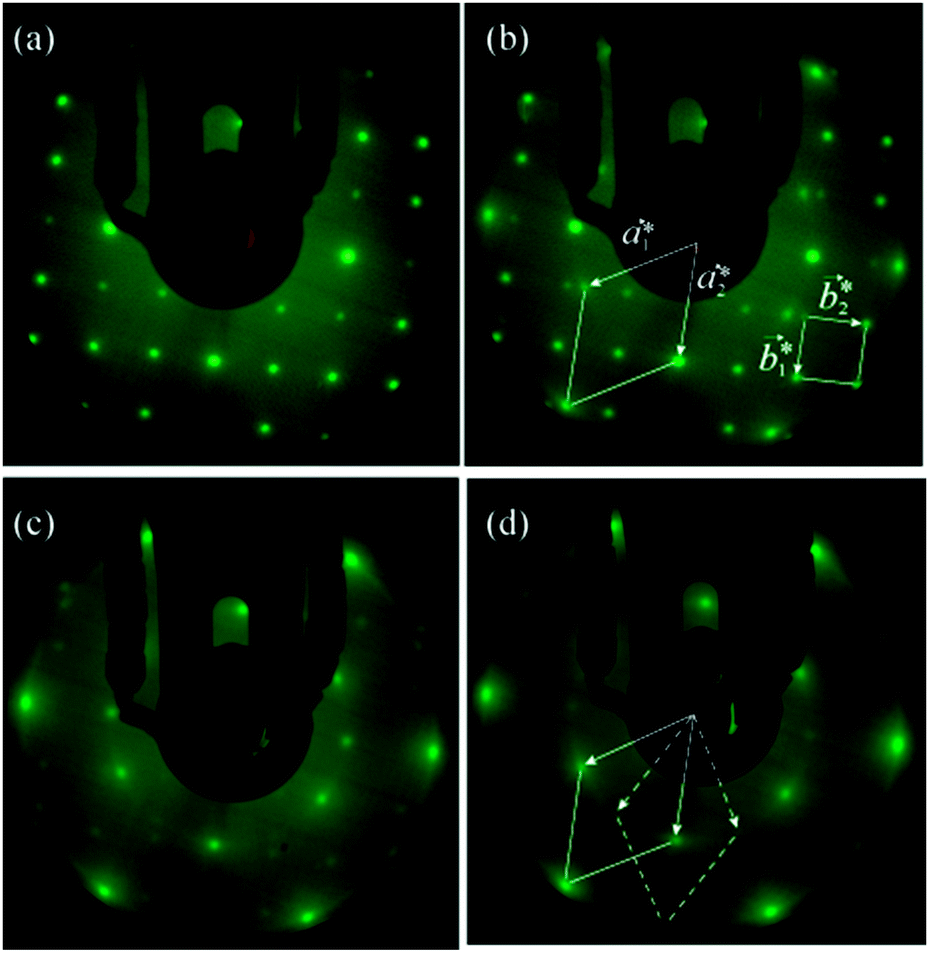 | ||
| Fig. 2 LEED patterns (150 eV) obtained after (a) 2 min (b) 7 min, (c) 9 min (d) 12 min deposition of Mo on FeS2{100}; the surface was flash annealed to 600 K after each deposition. Unit meshes and lattice vectors of the surface reciprocal lattices of MoS2(0001) and FeS2{100} (see text) are indicated in (b). Both primary and secondary (rotated by 30° from the latter) hexagonal patterns are indicated in (d). | ||
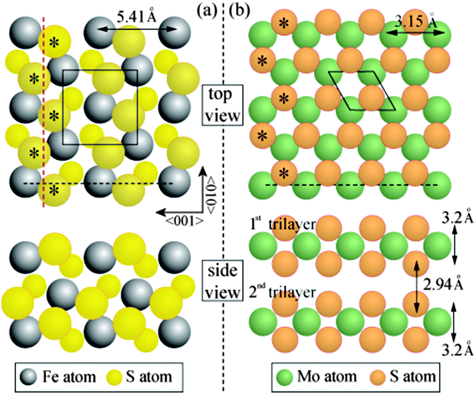 | ||
| Fig. 3 Ball models for (a) FeS2{100} and (b) and MoS2(0001) surface structures. The glide plane of the pyrite crystal is shown by the red broken line and is perpendicular to the page. The cross-sectional views along the grey broken lines are also plotted for each material. Asterisks mark the common S positions in the FeS2{100} and MoS2(0001) surface structures. | ||
With further Mo deposition, the hexagonal pattern gradually intensifies whilst the square pattern fades away. Fig. 2c corresponds to a total 9 min deposition time and a Mo/S Auger peak height ratio of 0.35. At this coverage the square pattern corresponding to the FeS2{100} surface has almost completely disappeared. The spots of the hexagonal pattern show some slight streaking suggestive of a ring diffraction pattern. Moreover, a second hexagonal pattern, rotated 30° with respect to the initial one is also visible (most obviously in the outer ring of spots, indicated in Fig. 2d; more clearly visible after image processing, ESI,† Fig. S1), albeit much less intense and more diffuse. The progressive disappearance of the original LEED pattern and intensification of the overlayer pattern are consistent with lateral growth of the MoS2(0001) regions until they cover the FeS2{100} substrate. In this case, our data suggest growth of MoS2 (0001) domains with both primary and secondary orientations rotated by 30° from each other.
After a cumulative Mo deposition time of 12 minutes (Mo/S = 0.46) only the hexagonal pattern is visible (Fig. 2d). This exposure lies beyond the break of slope in the Fe/S ratio in Fig. 1, corresponding to a reduction of 92% in the Fe/S ratio relative to the pristine FeS2{100} surface. The complete suppression of the square lattice corresponding to FeS2{100}, when probed at 150 eV electron kinetic energy, allows us to estimate the thickness of the MoS2 layer at that particular coverage as being of the order of 1 nm, based on the fact that measured attenuation lengths of electrons in this energy range are normally 1 nm or less in solids.15 The Auger electrons used to assess compositional changes were of comparable energies and therefore probe approximately the same depth. We note that the clear break of slope of the Fe/S peak height ratio implies completion of growth of a layer of uniform thickness after 9 min deposition.
Further Mo deposition beyond 12 minutes progressively led to a higher diffuse background in the hexagonal LEED pattern, and eventually to the loss of any diffraction pattern. This was accompanied by a continuing linear increase in the Mo/S Auger peak height ratio. These observations indicate that a disordered Mo-rich layer forms on top of the ordered MoS2 layer, rather than the overlayers stabilizing at an ordered stoichiometric MoS2(0001) structure. For exposures in excess of 12 minutes, longer anneals of up to 30 minutes were found to marginally sharpen the hexagonal LEED pattern, suggesting that S can diffuse through the Mo-rich overlayer, but with more difficulty than through the FeS2 substrate. In light of the arguments below, there is no reason in principle why a thicker epitaxial MoS2(0001) film should not form on FeS2{100}. The thickness of the ordered stoichiometric overlayer here is most likely S-diffusion-limited; we expect that co-deposition of S with Mo would be likely to lead to thicker epitaxial layers.
The formation of a thin film of MoS2 on the FeS2 substrate requires a driving force for S diffusion from one material to the other. Thermodynamically, MoS2 (Gibbs free energy of formation ΔfG°= −225.9 kJ mol−1) is more stable than FeS2 (ΔfG°= −166.9 kJ mol−1),16 which would drive S to react with deposited Mo and to form MoS2. A previous study by Kamaratos et al.17 of Fe adsorbed on MoS2{0001} found no evidence of Fe reacting with S from MoS2; at high temperatures Fe simply desorbs. This is consistent with the higher thermodynamic stability of MoS2 disfavouring diffusion of S from the MoS2 substrate to sulphurize Fe. The inverse process, by contrast, seems to be facilitated, on the evidence of our experiments.
As noted above, the LEED data indicate that MoS2(0001) grows epitaxially on FeS2{100}. This can be rationalised through the observation that the two materials share a common structural element. The structure of FeS2 is based on that of rocksalt (NaCl), with the centroids of persulphide S22− dimers located at anion sites, and the S–S dimer bonds oriented in 〈111〉 directions. This confers glide symmetry upon the {100} surface, and leads to planes of S atoms lying above and below each plane of Fe atoms, to form an S–Fe–S trilayer structure (Fig. 3(a)). MoS2 has a hexagonal crystal structure. S atoms are arranged hexagonally in both of two planes that lie above and below each plane of Mo atoms, to form an S–Mo–S trilayer structure (Fig. 3(b)); two trilayers are stacked within each bulk unit cell.
The relative orientation of the FeS2{100} and MoS2(0001) structures can be partially determined from the LEED patterns. The glide symmetry of FeS2{100} causes a characteristic pattern of systematic absences of alternate beams along the direction parallel to the glide line.18 This feature constrains the possible orientation of the substrate: for the LEED pattern shown in Fig. 2a, the glide line runs from top to bottom. Individual S–Fe–S trilayers lack rotational symmetry, but successive trilayers are related by 180° mutual rotation. Fig. 3a depicts one of the two trilayers in an orientation that corresponds to the LEED pattern It can be seen that the outer-lying S atoms in the top FeS2{100} trilayer are arranged in a zig-zag pattern. Fig. 3b depicts one trilayer of MoS2(0001); the orientation shown is consistent with that of the dominant hexagonal LEED pattern (Fig. 2b). The subset of S atoms marked * has an arrangement essentially identical to that of the zig-zag S rows of FeS2{100}: the period matches to within 1%.
If we now overlay the MoS2(0001) trilayer over the FeS2{100} trilayer such that the common zig-zag rows coincide (Fig. 4), it emerges that the structure comes back almost exactly into coincidence after three repeats of the FeS2{100} unit mesh (five of the MoS2(0001)) in the direction perpendicular to the common zig-zag S rows. A very slight elongation of the MoS2(0001) lattice in this direction (<3%) gives a perfect coincidence lattice structure. One possible scenario is that the common zig-zag row of S atoms is shared between the two structures, leading to S–Fe–S–Mo–S layering at the interface. Alternatively, both trilayers may be terminated by complete S layers, leading to S–Fe–S–S–Mo–S layering; in this scenario, the epitaxy is driven simply by van der Waals interactions between the layers. In principle, sourcing the S atoms in the MoS2 layer from the bulk FeS2 implies structural changes to the substrate. However, the quantity of S involved is negligible relative to the bulk concentration; moreover, we have previously shown that migration of bulk S to the surface facilitates self-healing of FeS2{100} after preferential S depletion during sputtering.12 We conclude that the substrate structure is not significantly altered by growth of the MoS2 film. Qualitative LEED observations cannot distinguish between the two suggested interface structures, but in either case it is the common zig-zag S rows that are the likely origin of the epitaxial growth that we observe. We emphasise that the well-defined epitaxial relationship between the two layers necessarily implies that the interface structure is crystallographically well defined.
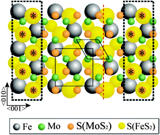 | ||
| Fig. 4 Approximate lattice match obtained by laying MoS2(0001) surface structure on top of FeS2{100} at the orientations determined by the LEED patterns in Fig. 2. The matching S positions are highlighted within the dotted rectangles. The unit meshes for MoS2(0001) and FeS2{100} are noted as diamonds and squares, respectively. FeS2 glide plane is shown by red dashed line. | ||
Given that successive FeS2{100} trilayers are mutually rotated by 180°, the MoS2(0001) overlayer (which has 3-fold, not 6-fold, rotational symmetry) may be correspondingly rotated on successive substrate terraces, leading to two rotational domains of a single structure. Alternatively, rotating the overlayer through 180° relative to the substrate produces a structure which is formally distinct but which preserves the coincidence of the zig-zag S rows. The hexagonal LEED pattern shows 6-fold symmetry in all rings of spots at all energies, indicating the superposition of two 3-fold-symmetric patterns rotated by 180° (ESI,† Fig. S2). This is consistent with two rotational domains of a single structure, or equally with coexistence of the two distinct structures.
Rotating the MoS2(0001) trilayer through 30° would change the orientation of the hexagonal LEED pattern to that of the subsidiary hexagonal pattern seen in Fig. 2d. As shown in Fig. S3 of the ESI,† this also allows some measure of coincidence between S atoms in the MoS2(0001) and FeS2{100} structures. However, fewer S atoms are common to both structures, and the lattice matching is poorer, than in the dominant orientation. These factors are likely reasons for this orientation being the subsidiary one.
Finally, we comment on the thickness, morphology and uniformity of the MoS2(0001) film. The LEED and AES data are consistent with an overlayer thickness that is of the order of 1 nm and is uniform (based on the clear AES break of slope). From the bulk lattice parameter of MoS2, c = 12.295 Å,14 and the fact that each unit cell contains two S–Mo–S trilayers, we can deduce that the MoS2(0001) film is most likely two, and certainly between one and three, trilayers thick (see ESI,† for justification of this assertion). Individual MoS2(0001) domains are at least of the order of 100 Å across. This is based on the fact that domains smaller than the LEED transfer width (usually taken to be of order 100 Å)15 would lead to interference effects not seen in our data. Measurements made at different points on the sample verify that the MoS2(0001) film has uniform characteristics across the macroscopic area of the sample (of order 1 cm2). The streaking seen in the LEED pattern implies slight rotational mosaicity of the MoS2(0001) layer. A similar effect is seen in LEED patterns obtained with graphene on Pt{111}19 and Cu{111}.20 This may relate to local distortions or structural imperfections within individual MoS2(0001) domains (as observed for graphene by Gao et al.19 and Vázquez de Parga et al.21), or to different azimuthal orientations of individual domains (as suggested for graphene by Avila et al.20).
In conclusion, few-layer films of highly ordered MoS2(0001) were formed on FeS2{100} by PVD of Mo and heating to 600 K to allow S to diffuse from the bulk substrate. The ordered MoS2(0001) overlayer was limited to a few layers’ thickness, most probably two S–Mo–S trilayers. We attribute the facile epitaxial growth to the ready availability of S from the pyrite substrate; a strong thermodynamic driving force for the formation of MoS2 in preference to FeS2/FeS; and the well-defined lattice relationship and common structural element between the MoS2(0001) and FeS2{100} surfaces. Grown this way, the MoS2 layer is already in intimate, crystallographically well-defined contact with the semiconducting substrate. This approach paves a promising possible way forward for the development of practical devices with 2D MoS2.
The authors thank the EPSRC (grant ref. EP/E039782/1) for funding.
Notes and references
- L. Rodríguez-Pérez, M. A. Herranz and N. Martín, Chem. Commun., 2013, 49, 3721 RSC.
- (a) R. Mas-Ballesté, C. Gómez-Navarro, J. Gómez-Herrero and F. Zamora, Nanoscale, 2011, 3, 20 RSC; (b) Q. H. Wang, K. Kalantar-Zadeh, A. Kis, J. N. Coleman and M. S. Strano, Nat. Nanotechnol., 2012, 7, 699 CrossRef CAS PubMed; (c) M. Xu, T. Liang, M. Shi and H. Chen, Chem. Rev., 2013, 113, 3766 CrossRef CAS PubMed.
- (a) W. O. Winer, Wear, 1967, 10, 422 CrossRef CAS; (b) M. Vrinat, M. Breysse, C. Geantet, J. Ramirez and F. Massoth, Catal. Lett., 1994, 26, 25 CrossRef CAS.
- B. Radisavljevic, A. Radenovic, J. Brivio, V. Giacometti and A. Kis, Nat. Nanotechnol., 2011, 6, 147 CrossRef CAS PubMed.
- (a) K. F. Mak, C. Lee, J. Hone, J. Shan and T. F. Heinz, Phys. Rev. Lett., 2010, 105, 136805 CrossRef; (b) A. Splendiani, L. Sun, Y. Zhang, T. Li, J. Kim, C.-Y. Chim, G. Galli and F. Wang, Nano Lett., 2010, 10, 1271 CrossRef CAS PubMed.
- (a) D. Xiao, G. B. Liu, W. Feng, X. Xu and W. Yao, Phys. Rev. Lett., 2012, 108, 196802 CrossRef; (b) H. Zeng, J. Dai, W. Yao, D. Xiao and X. Cui, Nat. Nanotechnol., 2012, 7, 490 CrossRef CAS PubMed; (c) K. F. Mak, K. He, J. Shan and T. F. Heinz, Nat. Nanotechnol., 2012, 7, 494 CrossRef CAS PubMed.
- W. Wu, L. Wang, Y. Li, F. Zhang, L. Lin, S. Niu, D. Chenet, X. Zhang, Y. Hao, T. F. Heinz, J. Hone and Z. L. Wang, Nature, 2014, 514, 470 CrossRef CAS PubMed.
- O. Frank and M. Kalbac, Chemical vapour deposition (CVD) growth of graphene films, in Graphene: Properties, Preparation, Characterisation and Devices, ed. V. Skákalová and A. B. Kaiser, Woodhead Publishing, 2014 Search PubMed.
- (a) Y. Zhan, Z. Liu, S. Najmaei, P. M. Ajayan and J. Lou, Small, 2012, 8, 966 CrossRef CAS PubMed; (b) Y.-H. Lee, X.-Q. Zhang, W. Zhang, M.-T. Chang, C.-T. Lin, K.-D. Chang, Y.-C. Lu, J. T.-W. Wang, C.-S. Chang, L.-J. Li and T.-W. Lin, Adv. Mater., 2012, 24, 2320 CrossRef CAS PubMed; (c) K.-K. Liu, W. Zhang, Y.-H. Lee, Y.-C. Lin, M.-T. Chang, C.-Y. Su, C.-S. Chang, H. Li, Y. Shi, H. Zhang, C.-S. Lai and L.-J. Li, Nano Lett., 2012, 12, 1538 CrossRef CAS PubMed; (d) Y. Shi, W. Zhou, A.-Y. Lu, W. Fang, Y.-H. Lee, A. L. Hsu, S. M. Kim, K. K. Kim, H. Y. Yang, L.-J. Li, J.-C. Idrobo and J. Kong, Nano Lett., 2012, 12, 2784 CrossRef CAS PubMed.
- (a) S. Helveg, J. V. Lauritsen, E. Lægsgaard, I. Stensgaard, J. K. Nørskov, B. S. Clausen, H. Topsøe and F. Besenbacher, Phys. Rev. Lett., 2000, 84, 951 CrossRef CAS; (b) J. Kibsgaard, J. V. Lauritsen, E. Lægsgaard, B. S. Clausen, H. Topsøe and F. Besenbacher, J. Am. Chem. Soc., 2006, 128, 13950 CrossRef CAS PubMed.
- A. K. Geim and I. V. Grigorieva, Nature, 2013, 499, 419 CrossRef CAS PubMed.
- (a) T. Liu, I. Temprano, S. J. Jenkins, D. A. King and S. M. Driver, Phys. Chem. Chem. Phys., 2012, 14, 11491 RSC; (b) T. Liu, I. Temprano, S. J. Jenkins, D. A. King and S. M. Driver, J. Phys. Chem. C, 2013, 117, 10990 CrossRef CAS.
- E. D. Stevens, M. L. DeLucia and P. Coppens, Inorg. Chem., 1980, 19, 813 CrossRef CAS.
- H. E. Swanson, N. T. Gilfrich and G. M. Ugrinic, NBS Circular 539, 1955, vol. 5 Search PubMed.
- D. P. Woodruff and T. A. Delchar, Modern Techniques of Surface Science, Cambridge University Press, 2nd edn, 1994 Search PubMed.
- CRC Handbook of Chemistry and Physics, ed. W. M. Haynes, Taylor and Francis, 95th edn, 2014 Search PubMed.
- M. Kamaratos and C. A. Papageorgopoulos, Surf. Sci., 1985, 160, 451 CrossRef CAS.
- B. Holland and D. P. Woodruff, Surf. Sci., 1973, 36, 488 CrossRef CAS.
- M. Gao, Y. Pan, L. Huang, H. Hu, L. Z. Zhang, H. M. Guo, S. X. Du and H.-J. Gao, Appl. Phys. Lett., 2011, 98, 033101 CrossRef PubMed.
- J. Avila, I. Razado, S. Lorcy, R. Fleurier, E. Pichonat, D. Vignaud, X. Wallart and M. C. Asenscio, Sci. Rep., 2013, 3, 8 Search PubMed.
- A. L Vázquez de Parga, F. Calleja, B. Borca, M. C. G. Passeggi, J. J. Hinarejos, F. Guinea and R. Miranda, Phys. Rev. Lett., 2008, 100, 056807 CrossRef.
Footnote |
| † Electronic supplementary information (ESI) available: Digitally enhanced and energy-dependent LEED data, schematic of subsidiary overlayer structure, electron attenuation length calculation. See DOI: 10.1039/c4cc06628f |
| This journal is © The Royal Society of Chemistry 2015 |