
 Open Access Article
 This Open Access Article is licensed under a
 Creative Commons Attribution 3.0 Unported Licence
Fine tuning of nanopipettes using atomic layer deposition for single molecule sensing†
Jasmine Y. Y.
Sze
a,
Shailabh
Kumar
bc,
Aleksandar P.
Ivanov
a,
Sang-Hyun
Oh
bc and
Joshua B.
Edel
*a
aDepartment of Chemistry, Imperial College London, Exhibition Road, South Kensington Campus, London SW7 2AZ, UK. E-mail: joshua.edel@imperial.ac.uk
bDepartment of Biomedical Engineering, University of Minnesota, Minneapolis, MN 55455, USA
cDepartment of Electrical and Computer engineering, University of Minnesota, Minneapolis, MN 55455, USA
First published on 3rd June 2015
Abstract
Nanopipettes are an attractive single-molecule tool for identification and characterisation of nucleic acids and proteins in solutions. They enable label-free analysis and reveal individual molecular properties, which are generally masked by ensemble averaging. Having control over the pore dimensions is vital to ensure that the dimensions of the molecules being probed match those of the pore for optimization of the signal to noise. Although nanopipettes are simple and easy to fabricate, challenges exist, especially when compared to more conventional solid-state analogues. For example, a sub-20 nm pore diameter can be difficult to fabricate and the batch-to-batch reproducibility is often poor. To improve on this limitation, atomic layer deposition (ALD) is used to deposit ultrathin layers of alumina (Al2O3) on the surface of the quartz nanopipettes enabling sub-nm tuning of the pore dimensions. Here, Al2O3 with a thickness of 8, 14 and 17 nm was deposited onto pipettes with a starting pore diameter of 75 ± 5 nm whilst a second batch had 5 and 8 nm Al2O3 deposited with a starting pore diameter of 25 ± 3 nm respectively. This highly conformal process coats both the inner and outer surfaces of pipettes and resulted in the fabrication of pore diameters as low as 7.5 nm. We show that Al2O3 modified pores do not interfere with the sensing ability of the nanopipettes and can be used for high signal-to-noise DNA detection. ALD provides a quick and efficient (batch processing) for fine-tuning nanopipettes for a broad range of applications including the detection of small biomolecules like RNA, aptamers and DNA–protein interactions at the single molecule level.
Introduction
Single-molecule detection in biomedical and biotechnological applications provides the opportunity to study individual molecules and identify rare events usually masked by ensemble averaging. One powerful technique to perform such studies in label-free conditions is nanopore sensing. In nanopore sensing1–3 individual biological analytes are translocated through a nanoscale pore in a thin insulating membrane and are identified by characteristic modulations in the nanopore current. Solid-state nanopores can be fabricated from various materials including SiNx,4–6 SiO2,7,8 graphene9,10 amongst others.11,12 A sub-class of solid-state nanopores, nanopipettes, are typically made from quartz or borosilicate glass and provide some advantages such as quick, low-cost fabrication,13 low-noise performance,14,15 chemical stability,16,17 easier handling, high-aspect ratio geometry and simple routes for multiplexed sensing.18 Due to these advantages, the use of nanopipettes has steadily increased in the detection of DNA,15,16,19–22 aptamers,23 proteins,24–26 nanoparticles27,28 and other bioanalytes, by modifying the pore surface13,24,29,30 and dimensions.18,31 Furthermore, they have been the probe of choice in high-resolution scanning ion conductance microscopy (SICM).32,33 Nanopipettes are typically fabricated by laser-assisted pulling, where a glass capillary is exposed to heating and pulling cycle(s), resulting in separation of the capillary into two sharp nanopipettes. Although it is possible to tune the pore dimensions by varying the pulling parameters (temperature, time, pulling strength, etc.), pore diameters below 20 nm are generally difficult to achieve. Ideally, significantly smaller nanopore diameters are needed in order to maximise signal-to-noise ratio in nanopore detection. Recently, shrinking of the pore diameter in nanopipettes by electron beam irradiation has been demonstrated,31 however, the shrinking process is relatively slow, expensive, and multiple pipettes cannot be processed simultaneously. An alternative approach as proposed in this article is to use atomic layer deposition (ALD), which allows for precise control with angstrom thick resolution to controllably alter the pore dimensions. Importantly, this is a batch process where depositions on multiple pipettes can be performed simultaneously. While ALD has been previously used for controllable shrinking in conventional planar solid-state nanopores,34–36 the benefits of ALD have not yet been translated to nanopipette platforms.Here we show that by depositing Al2O3 using ALD it is possible to controllably achieve multiple batches of coated nanopores with dimensions which are sub-10 nm in diameter. This brings the nanopipette dimensions into the same size regime as what is typically used in more conventional solid-state platforms. In addition to controlling nanopore dimensions, ALD functionalization of the nanopipettes allows for modification of the net charge on the nanopore surface. This is particularly useful for quartz and borosilicate glass nanopipettes which have high negative charge compared to conventional planar nanopores. Al2O3 has a net positive charge (at pH < 9)37 and ALD can be utilised to modify the interaction between the nanopore and the analyte. Due to ALD's excellent conformal deposition on high aspect ratio structures,38–41 both the inner and outer surfaces are coated which is advantageous when interaction between the nanopipette tip and the sample needs to be minimised (e.g. in SICM imaging and scanning applications).
Results and discussion
Two classes of quartz pipettes with starting pore diameters of, di = 75 ± 5 nm (type i) and dii = 25 ± 3 nm (type ii), were fabricated by laser-assisted pulling (see the Experimental section for details). This was followed by coating with films of Al2O3 using ALD (a schematic is shown in Fig. 1Bii). Al2O3 was chosen as the deposition material over other standard gases such as HfO2 as it has been well-studied and utilized extensively for conformal coating of diverse surfaces42–45 as well as its excellent dielectric properties, low capacitance,46 good adhesion and high electrical stability. Details on the ALD process are available in the Experimental section, Fig. S1 in the ESI† shows a schematic of the ALD deposition and images of ten pipettes placed inside the ALD chamber. Al2O3 was deposited on the pipettes at a rate of 5 Å per min. Al2O3 films with thickness of 8, 14 and 17 nm were deposited on the larger pipettes (type i) and layers with thickness of 5 and 8 nm on the smaller pipettes (type ii). For each deposition the Al2O3 thickness was confirmed by ellipsometry on silicon substrates adjacent to the nanopipettes. Images of both pipette types, before and after deposition were obtained by scanning electron microscopy (SEM). Fig. 1C shows representative SEM images of a nanopipette with a 25 nm nanopore before deposition and an image of a nanopipette of the same type after 8 nm Al2O3 deposition.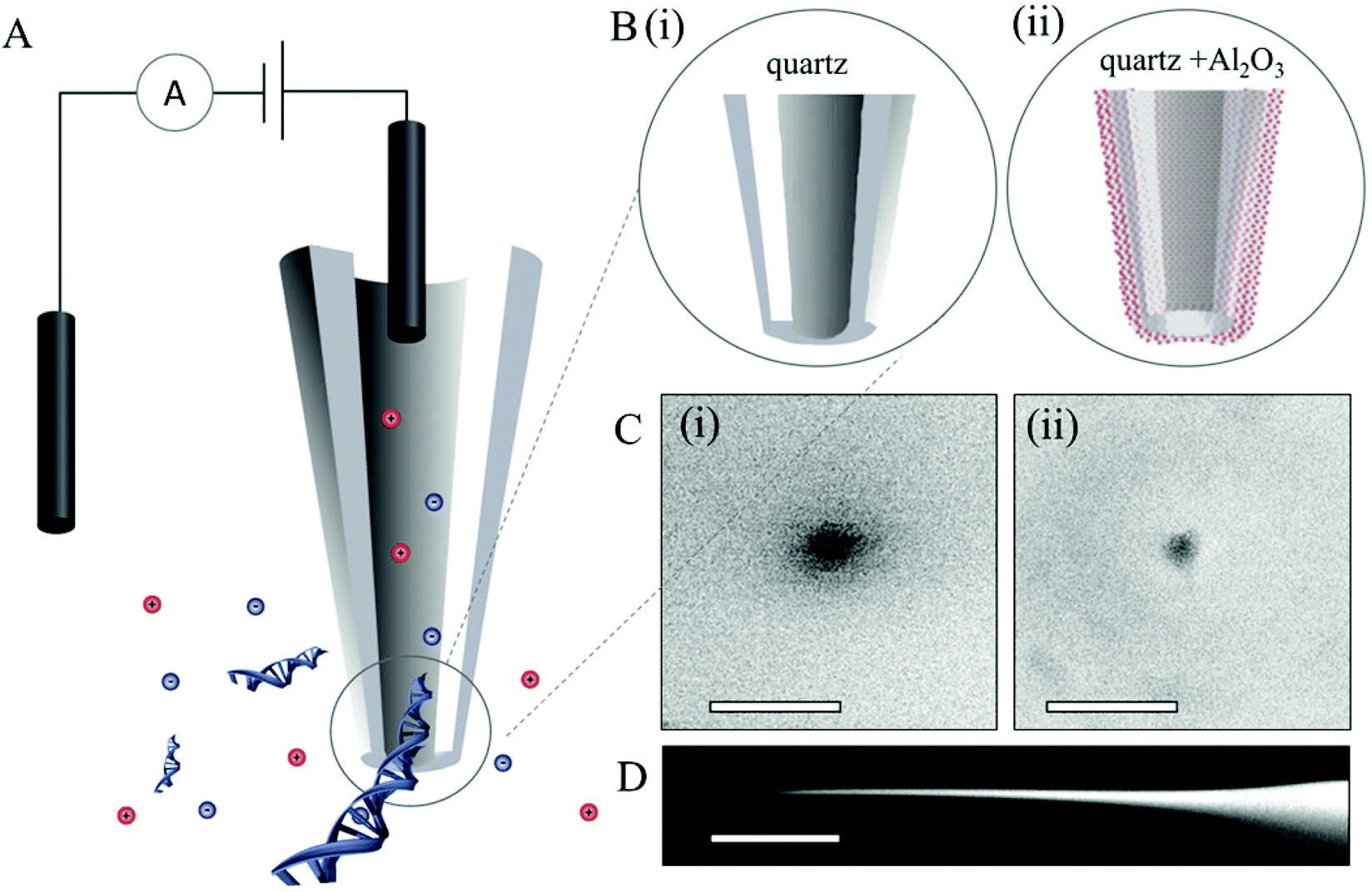 | ||
| Fig. 1 A. Schematic of the experimental set up with nanopipette. B. Zoomed in schematic of the tip end of the (i) unmodified pipette (ii) Al2O3ALD-modified pipette. C. SEM characterization of the pore diameter (i) 25 nm and (ii) 7.5 nm. The scale bars are 40 nm. D. SEM image of the nanopipette tip (scale bar is 200 μm). | ||
ALD coating was further confirmed by ionic current measurements. Ionic transport across the nanopores of both coated and non-coated nanopipette was characterised in 1 M KCl, 10 mM Tris, 1 mM EDTA, pH 8 solution (schematic shown in Fig. 1A). For each nanopipette, multiple chronoamperometric traces (ranging from −500 mV to 500 mV with a 50 mV step) were measured using an Axopatch 200B patch-clamp amplifier. I–V curves were extracted from the chronoamperometric traces. Fig. 2A shows I–V traces average for 60 pipettes for both types of pipettes before and after the ALD coating. All coated pipettes showed linear I–V (no rectification) indicating no preferential direction for the ion flow. For both nanopipette types the nanopore current (and conductance) systematically decreased with increasing thickness of the Al2O3 coating, indicating a decrease in nanopore diameter. To estimate the pore diameter we used the model described by Steinbock et al.47 (eqn (1), in ESI S2†). Due to the high ionic strength of the solution used (1 M KCl), surface conductivity contributions to the conductance were neglected. For uncoated pipettes average conductance of 252 ± 16 nS (type i) and 58 ± 5 nS (type ii) were obtained (all error estimates are standard deviations), corresponding to calculated pore diameters of 75 ± 5 nm and 25 ± 3 nm respectively. These values are in agreement with the pore diameters of 82 ± 5 nm and 27 ± 3 nm, measured by SEM imaging. The pore conductance model also provided good agreement between the calculated pore diameter and SEM measurements for ALD coated nanopipettes for both pipette types. Fig. 2B shows plots of pore diameters both calculated from eqn (1), in ESI S2† and from SEM measurements indicating that the diameter of the nanopore decreased linearly with the thickness of deposited Al2O3.
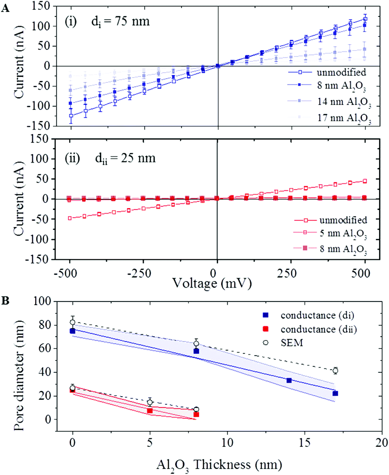 | ||
| Fig. 2 A (i) I–V characteristics of uncoated and coated (8, 14 and 17 nm Al2O3 deposition) pipettes from di. (ii) I–V characteristics of uncoated and coated (5 and 8 nm Al2O3 deposition) pipettes from dii. The average I–V curve across the unmodified pipettes was measured with thirty pipettes on both di and dii and all thickness of Al2O3 deposition were measured with ten pipettes. The error bars as presented are the standard deviation in the current between individual devices at each voltage from −500 to 500 mV. B The pipette pore diameter is plotted as a function of the thickness of the deposited Al2O3 layer, as measured on a planar Si substrate: conductance from type (di and dii) and the average of these devices are shown in (square) and the shaded area (blue and red) represents one standard deviation. The second part which the coated pipette is measured by SEM (circle) (mean value ± one standard deviation). The diameter of a minimum of ten pipettes at each of the deposition thicknesses of 5, 8, 14 and 17 nm was measured. | ||
Traditionally, the relationship between Al2O3 ALD rate and thickness has been modelled on a flat Si substrate and has been confirmed by in situ FTIR42,43 and mass spectrometry.44 While in Fig. 2B the thickness of the deposited Al2O3 was measured on a planar Si substrate, different thicknesses deposited in a pore can be expected due to the different surface chemistry of the pipette and its high-aspect conical geometry. Indeed the rate of shrinking of the nanopore diameters was measurably higher than the rate of deposition on planar Si samples. During the ALD process we expect a 2 nm reduction in the pore diameter with every 1 nm of Al2O3 deposition, or conversely, a slope of ∼2 for the plots presented in Fig. 2B. Instead we measured higher deposition ratios of 3.0 ± 0.3 for type (i) and 2.9 ± 0.8 for type (ii) pipettes. One possible explanation is the change in the reaction conditions inside the nanopipette. The Al2O3 ALD growth occurs during alternating exposures to TMA and H2O. The growth per cycle is dependent on the surface species and surface chemistry.42,48,49 During the ALD process, precursor gases are pumped in the chamber sequentially, and react on the surface to form oxide films. Flow through the confined geometry of nanopipette may affect the reaction rate at the surface. In addition, difference in the surface conditions such as availability of nucleation sites can lead to change in amount of deposited Al2O3.50
The ALD coating adds additional dielectric layer, although with higher dielectric constant and dielectric loss factor (ε = 3.8 and Dloss = ∼10−4 for quartz and ε = 9.1 and Dloss = ∼2 × 10⁻⁴ for Al2O3). The non-coated pipettes showed ∼10 pA root mean square (RMS) current noise at 300 mV, at 10 KHz filtering. The noise performance remained very similar for the coated ALD pipettes with 4.1, 9.8 and 9.7 pA rms current noise, respectively for pipettes coated after 8, 14 and 17 nm Al2O3 deposition. Power spectrum density (PSD) plots of these pipettes are presented in ESI S3.†
To demonstrate the functionality and investigate how the deposited Al2O3 affects the surface properties of the pipettes, DNA translocation experiments were carried out on ALD-modified nanopores (with diameters of 60 and 7.5 nm). Fig. 3A shows a representative current trace of single-molecule detection of 10 kbp dsDNA with a 7.5 nm pore (similar data for a 60 nm pore are shown in S3A†). The chronoamperometric trace shows characteristic ionic current blockades due to the translocation of the DNA molecules across the pore. Fig. 3B displays an expanded view of 5 representative translocation events. Additional current traces (for different potentials) and current dwell time scatter plots are available respectively in S4 and S5 in the ESI.†
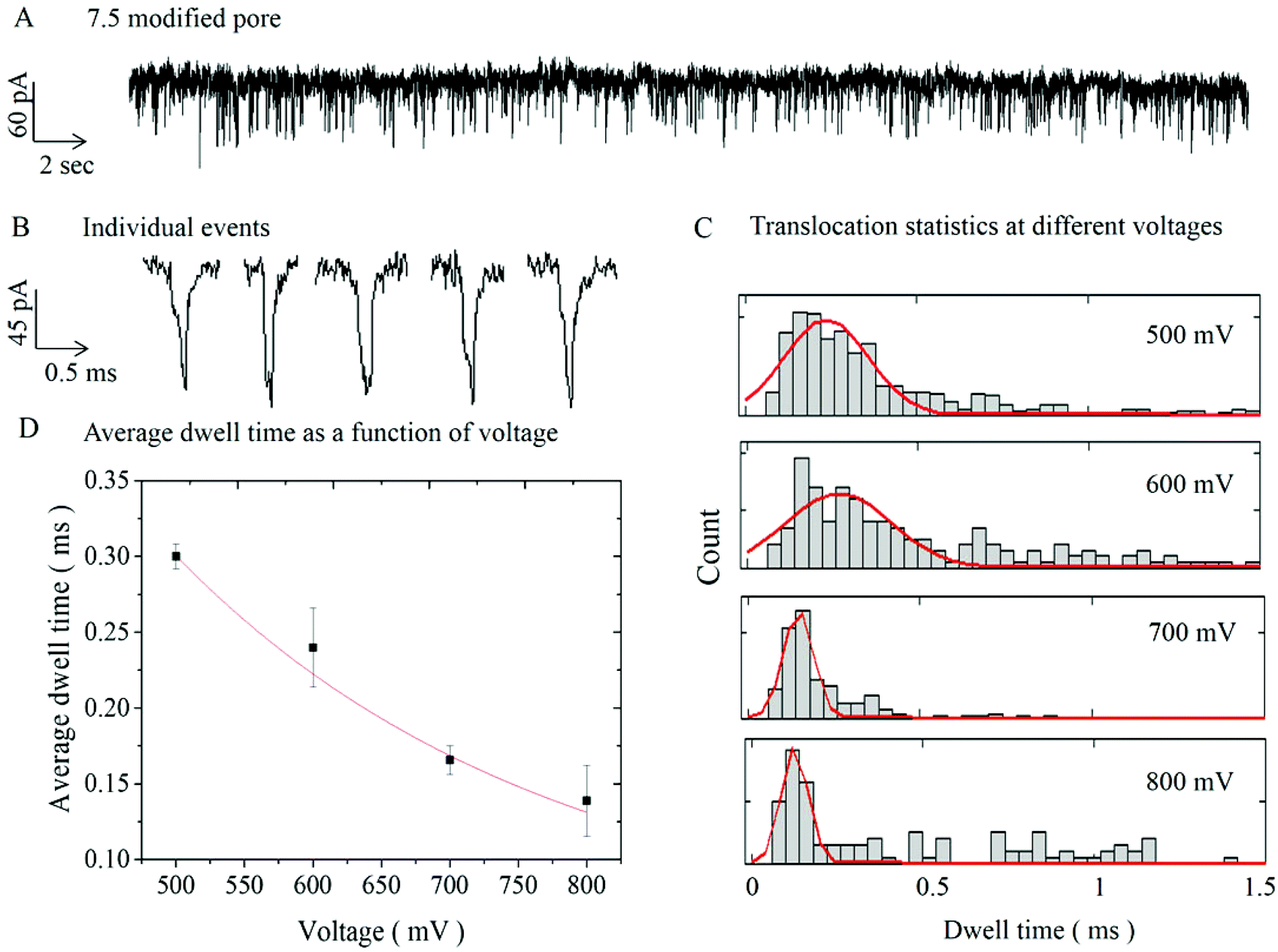 | ||
| Fig. 3 A Typical current trace on 7.5 nm modified pores after the addition of 100 pM of 10 kbp DNA at 300 mV. Discrete drops in the ion current are clearly observed and corresponding to pore blockades due to the translocation of DNA molecules. B Representative single molecule events on expanded scale. C Histograms of the dwell time distribution for applied voltages from 500–800 mV. D Average dwell time of the modified pore as a function of voltage and the red line showed exponential fit to the data. The average dwell times were 0.30 ± 0.01, 0.24 ± 0.03, 0.17 ± 0.01 and 0.14 ± 0.02 ms, respectively, for 500, 600, 700, 800 mV. | ||
Experiments of 10 kbp dsDNA translocation through both 60 nm and 7.5 nm diameter pores were performed for range of applied voltage (300–600 mV) and (500–800 mV) respectively, as shown in Fig. 3C and S3C.† The results indicated lower average dwell time with increasing applied voltage. This is as expected, since higher applied voltage results in stronger electrophoretic driving force exerted on the DNA molecules, leading to higher translocation velocities and shorter dwell times.39,47,51,52Fig. 3C shows dwell time histograms at different applied voltages for 7.5 nm pore, (for 60 nm pore data is available in S3C†). Each distribution was fitted with a first-passage probability density function (FP-PDF) as reported by Ling et al.53 The FP-PDF is defined by F(t) = (L/(4πDt3)1/2e−(L − υt)2/4Dt where D is the diffusion constant, υ is the drift velocity, and L is the contour length of the DNA. Slightly longer dwell time and larger peak current were observed with the 7.5 nm pore (0.30 ± 0.01 ms, 122. 4 ± 8.9 pA), compared to (0.24 ± 0.02 ms, 95.4 ± 5.6 pA) for the larger 60 nm pore (see S3, ESI†). This can be explained by a stronger DNA–pore interaction in smaller pores.54,55 In general, the dwell time and the peak current for 10 kbp DNA were in good agreement with literature values for non-modified solid-state nanopores and nanopipettes.2,5,19 The average dwell time for a 7.5 nm pore at 500 mV was 0.30 ± 0.01 ms, which corresponds to a translocation speed of 11.2 ± 0.4 mm s−1. Again, these results are in good agreement with the ones reported by Steinbock et al. (10.3 mm s−1),16 by Li et al. (10 mm s−1),5 and by Gong et al. (8.2 mm s−1).19 Finally the calculated the excluded ionic charge per translocation event for was 16.9 ± 4.0 fAs and 23.5 ± 12.7 fAs respectively for 60 nm and 7.5 nm pores. These values were found to be in the same order of magnitude as those previously reported in the literature.16,19
For the smaller, 7.5 nm pores, translocation events were observed only for potential above 500 mV. This threshold applied potential required to drive the DNA molecule through the pore, suggests the presence of an entropic barrier. Fig. 3D shows a non-linear decrease of dwell time with increasing voltage, supporting the presence of such barrier during the DNA transport across the pore.34,39 In addition for smaller pores, small sub-population events with longer dwell times (>0.5 ms) were observed indicating there is a DNA–modified pore interaction, similar to the effect seen in small solid-state nanopores.54
Conclusions
The results confirmed that Al2O3 ALD can be used to fine tune nanopipettes to sub 10s nm without interfering with the pore's sensing abilities. The process only requires application of higher electrophoretic force to overcome the entropic barrier and drive the molecules through the narrow nanopores. We also demonstrated that ALD can be used for batch reduction of nanopipette pore size without any other expensive fabrication facilities. The nanopipettes were fabricated in sub-10s nm and demonstrated good agreement on the translocation times, peak current and excluded ionic charge with results reported for small solid-state nanopores in literature. The modified nanopipettes were characterised using SEM and the images were in good agreement with the electrical data. We also performed voltage dependent translocation studies and showed that translocation times were not affected by the Al2O3 modification of pores. Although these modified nanopipettes with reduced pore size offer many advantages, detection using sub-nm pore requires further studies analysing complexities arising due to the confined geometry in the nanopipette. It should be mentioned that ALD is a chemistry driven process hence the deposition result and nanopore performance may vary for difference choice of precursor – substrate systems. Deposition from different precursors would require further investigation, however they can potentially enable modified nanopipette with enhanced surface properties. In the near future, the Al2O3 ALD modification can allow detection of smaller molecule sequences or other molecules like RNA to meet the requirements of many different applications and certainly provides a step closer to scale-up in advancing sensing technology.Methods
Fabrication of nanopipette
A thin glass capillary (Intracel Ltd, UK) length 75 mm with 0.6 mm filament was placed inside the plasma cleaner to ensure all dusts and dirt are removed. After plasma-cleaning, the capillary was placed in a laser-based pipette puller (Sutter Instrument, P-2000). The pipette pulling occurred in two-stage process with stage 1 [Heat:575; Fil:3, Vel:3, Del:145, Pull:75] and pulled a 1.2 mm taper into the capillary before stage 2 [Heat:600; Fil:0, Vel:15, Del:128, Pull:200]. After fabrication, ALD Al2O3 was deposited on the nanopipettes. For fabrication of the second batch of pipettes with smaller starting diameter (dii = 25 ± 3 nm), we used 75 mm long capillary with 0.5 mm filament, followed by plasma-cleaning and placement into the pipette puller. The first pipette pulling stage [Heat:575; Fil:3, Vel:35, Del:145, Pull:75] and pulls a 1.7 mm taper into the capillary before stage 2 [Heat:700; Fil:0, Vel:15, Del:128, Pull:200]. It should be noted that there is some variation between P2000 pullers due to local temperature and humidity therefore these pulling parameters only serve as an example.ALD deposition
The nanopipettes were further plasma cleaned prior to ALD deposition. The nanopipettes were coated with 5, 8, 14 and 17 nm calculated thickness of alumina (Al2O3) using atomic layer deposition (ALD, Savannah, Cambridge Nanotech) at 235 °C. Al2O3 has been widely used in the thin film deposition, as the deposited layer is thermally and chemically stable and exhibits negligible ion diffusion. Trimethylaluminium (TMA) and water vapour were injected sequentially in the chamber with nitrogen (N2) purging in between the injections. The deposition rate was around 1.1 A° per cycle. Silicon wafers were placed in the chamber along with the nanopipettes and ellipsometry was performed for calibration and checking the thickness of deposited alumina layer.Solutions and reagents
The buffer solution was made using 1 M KCl, 10 mM Tris and 1 mM EDTA (pH 8). 10 kbp DNA (New England Biolabs) was used for the translocation studies. All DNA samples were diluted to a final concentration of 100 pM in the buffered solution and filtered using a 0.2 μm filter.Ion current measurement and detection
Ionic current characterisations of the nanopipettes and translocation experiments were carried out with an Axopatch 200B patch clamp current amplifier (Molecular Devices, USA). An Ag/AgCl electrode was inserted into the nanopipette (patch electrode) and in the external reservoir (bath/ground electrode) at positive bias DNA was translocated from the bath towards the interior of the nanopipette. The recorded data was filtered using a 10 kHz, 4-pole Bessel low pass filter. The recorded data was digitized with a Digidata 1440A at 50 kHz was then processed using custom written Matlab code.Acknowledgements
JBE acknowledges the ERC for a starting investigator grant and the BBSRC for financial support. S.K. and S.-H.O. acknowledge funding from the U.S. National Science Foundation (NSF CAREER Award). This work utilized resources at the University of Minnesota, including the Minnesota Nanofabrication Center, which receives partial support from NSF through the National Nanotechnology Infrastructure Network program.References
- B. N. Miles, A. P. Ivanov, K. A. Wilson, F. Dogan, D. Japrung and J. B. Edel, Chem. Soc. Rev., 2013, 42, 15–28 RSC.
- C. Dekker, Nat. Nanotechnol., 2007, 2, 209–215 CrossRef CAS PubMed.
- D. G. Haywood, A. Saha-Shah, L. A. Baker and S. C. Jacobson, Anal. Chem., 2015, 87, 172–187 CrossRef CAS PubMed.
- M. J. Kim, M. Wanunu, D. C. Bell and A. Meller, Adv. Mater., 2006, 18, 3149–3153 CrossRef CAS PubMed.
- J. Li, M. Gershow, D. Stein, E. Brandin and J. A. Golovchenko, Nat. Mater., 2003, 2, 611–615 CrossRef CAS PubMed.
- D. S. Jiali Li, C. McMullan, D. Branton, M. J. Aziz and J. A. Golovchenko, Nature, 2001, 412, 166–169 CrossRef PubMed.
- J. H. C. A. J. Storm, X. S. Ling, H. W. Zandbergen and C. Dekker, Nat. Mater., 2003, 2, 537–540 CrossRef PubMed.
- H. Chang, F. Kosari, G. Andreadakis, M. Alam, G. Vasmatzis and R. Bashir, Nano Lett., 2004, 4, 1551–1556 CrossRef CAS.
- G. g. F. Schneider, S. W. Kowalczyk, V. E. Calado, G. g. Pandraud, H. W. Zandbergen, L. M. K. Vandersypen and C. Dekker, Nano Lett., 2010, 10, 3163–3167 CrossRef CAS PubMed.
- C. A. Merchant, K. Healy, M. Wanunu, V. Ray, N. Peterman, J. Bartel, M. D. Fischbein, K. Venta, Z. Luo, A. T. C. Johnson and M. Drndić, Nano Lett., 2010, 10, 2915–2921 CrossRef CAS PubMed.
- J. B. Heng, C. Ho, T. Kim, R. Timp, A. Aksimentiev, Y. V. Grinkova, S. Sligar, K. Schulten and G. Timp, Biophys. J., 2004, 87, 2905–2911 CrossRef CAS PubMed.
- M. Ayub, A. Ivanov, J. Hong, P. Kuhn, E. Instuli, J. B. Edel and T. Albrecht, J. Phys.: Condens. Matter: an Institute of Physics journal, 2010, 22, 454128 CrossRef PubMed.
- P. Actis, A. C. Mak and N. Pourmand, Bioanal. Rev., 2010, 1, 177–185 CrossRef PubMed.
- R. A. Levis and J. L. Rae, Biophys. J., 1993, 65, 1666–1677 CrossRef CAS.
- L. J. Steinbock, R. D. Bulushev, S. Krishnan, C. Raillon and A. Radenovic, ACS Nano, 2013, 7, 11255–11262 CrossRef CAS PubMed.
- L. J. Steinbock, O. Otto, C. Chimerel, J. Gornall and U. F. Keyser, Nano Lett., 2010, 10, 2493–2497 CrossRef CAS PubMed.
- R. J. White, E. N. Ervin, T. Yang, X. Chen, S. Daniel, P. S. Cremer and H. S. White, J. Am. Chem. Soc., 2007, 129, 11766–11775 CrossRef CAS PubMed.
- N. A. Bell, V. V. Thacker, S. Hernández-Ainsa, M. E. Fuentes-Perez, F. Moreno-Herrero, T. Liedl and U. F. Keyser, Lab Chip, 2013, 13, 1859–1862 RSC.
- X. Gong, A. V. Patil, A. P. Ivanov, Q. Kong, T. Gibb, F. Dogan, A. J. deMello and J. B. Edel, Anal. Chem., 2014, 86, 835–841 CrossRef CAS PubMed.
- B. Zhang, M. Wood and H. Lee, Anal. Chem., 2009, 81, 5541–5548 CrossRef CAS PubMed.
- A. P. Ivanov, P. Actis, P. Jönsson, D. Klenerman, Y. Korchev and J. B. Edel, ACS Nano, 2015, 9, 3587–3595 CrossRef CAS PubMed.
- T. R. Gibb, A. P. Ivanov, J. B. Edel and T. Albrecht, Anal. Chem., 2014, 86, 1864–1871 CrossRef CAS PubMed.
- P. Actis, A. Rogers, J. Nivala, B. Vilozny, R. A. Seger, O. Jejelowo and N. Pourmand, Biosens. Bioelectron., 2011, 26, 4503–4507 CrossRef CAS PubMed.
- S. Ding, C. Gao and L.-Q. Gu, Anal. Chem., 2009, 81, 6649–6655 CrossRef CAS PubMed.
- W. Li, N. A. W. Bell, S. Hernández-Ainsa, V. V. Thacker, A. M. Thackray, R. Bujdoso and U. F. Keyser, ACS Nano, 2013, 7, 4129–4134 CrossRef CAS PubMed.
- L. J. Steinbock, S. Krishnan, R. D. Bulushev, S. Borgeaud, M. Blokesch, L. Feletti and A. Radenovic, Nanoscale, 2014, 6, 14380–14387 RSC.
- M. Karhanek, J. T. Kemp, N. Pourmand, R. W. Davis and C. D. Webb, Nano Lett., 2005, 5, 403–407 CrossRef CAS PubMed.
- W.-J. Lan, D. A. Holden, B. Zhang and H. S. White, Anal. Chem., 2011, 83, 3840–3847 CrossRef CAS PubMed.
- S. Umehara, N. Pourmand, C. D. Webb, R. W. Davis, K. Yasuda and M. Karhanek, Nano Lett., 2006, 6, 2486–2492 CrossRef CAS PubMed.
- Y. Fu, H. Tokuhisa and L. A. Baker, Chem. Commun., 2009, 4877–4879 RSC.
- L. Steinbock, J. Steinbock and A. Radenovic, Nano Lett., 2013, 13, 1717–1723 CrossRef CAS.
- P. Novak, C. Li, A. I. Shevchuk, R. Stepanyan, M. Caldwell, S. Hughes, T. G. Smart, J. Gorelik, V. P. Ostanin, M. J. Lab, G. W. J. Moss, G. I. Frolenkov, D. Klenerman and Y. E. Korchev, Nat. Methods, 2009, 6, 279–281 CrossRef CAS PubMed.
- A. I. Shevchuk, G. I. Frolenkov, D. Sánchez, P. S. James, N. Freedman, M. J. Lab, R. Jones, D. Klenerman and Y. E. Korchev, Angew. Chem., Int. Ed., 2006, 118, 2270–2274 CrossRef PubMed.
- P. Chen, J. Gu, E. Brandin, Y.-R. Kim, Q. Wang and D. Branton, Nano Lett., 2004, 4, 2293–2298 CrossRef CAS PubMed.
- Y.-R. Kim, J. Min, I.-H. Lee, S. Kim, A.-G. Kim, K. Kim, K. Namkoong and C. Ko, Biosens. Bioelectron., 2007, 22, 2926–2931 CrossRef CAS PubMed.
- B. M. Venkatesan, B. Dorvel, S. Yemenicioglu, N. Watkins, I. Petrov and R. Bashir, Adv. Mater., 2009, 21, 2771–2776 CrossRef CAS PubMed.
- M. Kosmulski, J. Colloid Interface Sci., 2002, 253, 77–87 CrossRef CAS PubMed.
- P. Chen, T. Mitsui, D. B. Farmer, J. Golovchenko, R. G. Gordon and D. Branton, Nano Lett., 2004, 4, 1333–1337 CrossRef CAS PubMed.
- B. M. Venkatesan, A. B. Shah, J.-M. Zuo and R. Bashir, Adv. Funct. Mater., 2010, 20, 1266–1275 CrossRef CAS PubMed.
- B. M. Venkatesan, D. Estrada, S. Banerjee, X. Jin, V. E. Dorgan, M.-H. Bae, N. R. Aluru, E. Pop and R. Bashir, ACS Nano, 2012, 6, 441–450 CrossRef CAS PubMed.
- S. M. George, Chem. Rev., 2009, 110, 111–131 CrossRef PubMed.
- A. C. Dillon, A. W. Ott, J. D. Way and S. M. George, Surf. Sci., 1995, 322, 230–242 CrossRef CAS.
- J. Ferguson, A. Weimer and S. George, Thin Solid Films, 2000, 371, 95–104 CrossRef CAS.
- M. Juppo, A. Rahtu, M. Ritala and M. Leskelä, Langmuir, 2000, 16, 4034–4039 CrossRef CAS.
- M. D. Groner, J. W. Elam, F. H. Fabreguette and S. M. George, Thin Solid Films, 2002, 413, 186–197 CrossRef CAS.
- J. Yota, H. Shen and R. Ramanathan, J. Vac. Sci. Technol., A, 2013, 31, 01A134 Search PubMed.
- L. J. Steinbock, A. Lucas, O. Otto and U. F. Keyser, Electrophoresis, 2012, 33, 3480–3487 CrossRef CAS PubMed.
- S. M. George, A. W. Ott and J. W. Klaus, J. Phys. Chem., 1996, 100, 13121–13131 CrossRef CAS.
- A. W. Ott, J. W. Klaus, J. M. Johnson and S. M. George, Thin Solid Films, 1997, 292, 135–144 CrossRef CAS.
- C. A. Wilson, R. K. Grubbs and S. M. George, Chem. Mater., 2005, 17, 5625–5634 CrossRef CAS.
- A. Meller, L. Nivon and D. Branton, Phys. Rev. Lett., 2001, 86, 3435–3438 CrossRef CAS.
- S. W. Kowalczyk, M. W. Tuijtel, S. P. Donkers and C. Dekker, Nano Lett., 2010, 10, 1414–1420 CrossRef CAS PubMed.
- D. Y. Ling and X. S. Ling, J. Phys.: Condens. Matter: an Institute of Phys. J., 2013, 25, 375102 CrossRef PubMed.
- S. Carson, J. Wilson, A. Aksimentiev and M. Wanunu, Biophys. J., 2014, 107, 2381–2393 CrossRef CAS PubMed.
- R. Akahori, T. Haga, T. Hatano, I. Yanagi, T. Ohura, H. Hamamura, T. Iwasaki, T. Yokoi and T. Anazawa, Nanotechnology, 2014, 25, 275501 CrossRef PubMed.
Footnote |
| † Electronic supplementary information (ESI) available. See DOI: 10.1039/c5an01001b |
| This journal is © The Royal Society of Chemistry 2015 |