
 Open Access Article
 This Open Access Article is licensed under a
 Creative Commons Attribution 3.0 Unported Licence
Reconstructing accurate ToF-SIMS depth profiles for organic materials with differential sputter rates†
Adam J.
Taylor
 ab,
Daniel J.
Graham
ac and
David G.
Castner
*abc
ab,
Daniel J.
Graham
ac and
David G.
Castner
*abc
aNational ESCA and Surface Analysis Center for Biomedical Problems (NESAC/BIO), Molecular Engineering and Sciences Institute, University of Washington, Seattle, WA, USA. E-mail: castner@uw.edu; Tel: +1 206-543-8094
bDepartment of Chemical Engineering, University of Washington, Seattle, WA, USA
cDepartment of Bioengineering, University of Washington, Seattle, WA, USA
First published on 10th July 2015
Abstract
To properly process and reconstruct 3D ToF-SIMS data from systems such as multi-component polymers, drug delivery scaffolds, cells and tissues, it is important to understand the sputtering behavior of the sample. Modern cluster sources enable efficient and stable sputtering of many organics materials. However, not all materials sputter at the same rate and few studies have explored how different sputter rates may distort reconstructed depth profiles of multicomponent materials. In this study spun-cast bilayer polymer films of polystyrene and PMMA are used as model systems to optimize methods for the reconstruction of depth profiles in systems exhibiting different sputter rates between components. Transforming the bilayer depth profile from sputter time to depth using a single sputter rate fails to account for sputter rate variations during the profile. This leads to inaccurate apparent layer thicknesses and interfacial positions, as well as the appearance of continued sputtering into the substrate. Applying measured single component sputter rates to the bilayer films with a step change in sputter rate at the interfaces yields more accurate film thickness and interface positions. The transformation can be further improved by applying a linear sputter rate transition across the interface, thus modeling the sputter rate changes seen in polymer blends. This more closely reflects the expected sputtering behavior. This study highlights the need for both accurate evaluation of component sputter rates and the careful conversion of sputter time to depth, if accurate 3D reconstructions of complex multi-component organic and biological samples are to be achieved. The effects of errors in sputter rate determination are also explored.
Introduction
The capability of argon gas cluster ion beam (GCIB) sources to effectively sputter organic materials with minimal surface damage has expanded the range of systems that may be studied by ToF-SIMS sputter depth profiling and 3D imaging. These include multicomponent organic systems that form key components of diverse technologies including organic photovoltaics1 drug eluting stents2,3 and model polymeric multilayer systems.4,5 Argon cluster sources have proved similarly valuable for the analysis of biological materials such as amino acids,6 lipids7 and peptides.8 Analysis by ToF-SIMS has the potential to provide useful information about the composition, dimensions and spatial locations of features, interfaces and defects in such systems. However, answering questions about these systems requires accurate calibration and scaling along the z-axis (depth) during analysis of depth profiles and 3D images. When a uniform sputter rate through the sample, including the substrate, may be assumed, depth profile calibration can be performed by simply calculating a single sputter rate based on the time to sputter to the location of a known feature. The location of other features and interfaces can then be inferred directly from the sputter time required to reach the area of interest. However, many organic materials sputter at different rates.9,10 Such differences in sputtering may introduce a number of artifacts, which require careful consideration during data reconstruction. These include the distortion of apparent feature dimensions and spatial locations. These artifacts become more pronounced as the difference in sputter rates increases.The analysis and reconstruction of depth profiles has been of interest to researchers using both XPS and SIMS. Of particular interest is the ability to determine interface and delta layer positions within multilayer or mixed systems.11–14 Several studies have described the need for, and methods of, correcting for a number of depth profiling artifacts. These include changing sputter rates in highly topographic samples,15 and beam-damage induced sputter rate deterioration.16,17 However, few studies have used methods to identify and correct for different component sputter rates.18,19 In some cases differences in sputter rates may be minimized through careful selection of cluster size and energy.9 However, this may not provide sufficient range of sputter-rate manipulation. Approaches to dynamically measure sputter yield, through a quartz crystal microbalance10 or secondary neutral mass spectrometry,20 have been proposed. More simply, correction for different sputter rates can be applied during depth calibration using component sputter rates calculated from single-component films. This study demonstrates the application and value of such post-hoc correction in a spun-cast polystyrene–PMMA bilayer system. This polymer pairing was selected due to its previously demonstrated differences in sputter rate.9
In this study we demonstrate that (1) when differences in sputter rates between components are not taken into account reconstructed depth profiles are inaccurate; (2) application of individual component sputter rates allows for accurate depth profiles to be transformed from sputter time/dose to depth; (3) accounting for the transition between different sputter rates across an interface may further improve profile reconstruction; and (4) that small deviations in sputter rate determination can have significant effects on the reconstructed depth profile.
Results and discussion
Characterization of single-component and bilayer films
Thin polymer films of polystyrene and PMMA, and bilayers of polystyrene on PMMA, were prepared by spin-casting from selective solvents. XPS analysis of single-component and bilayer films was performed to validate composition of single component films and assess continuity of the polystyrene overlayer in bilayer films. XPS spectra and calculated atomic percentages for both polystyrene and PMMA are in agreement with those previously reported for these materials.21–24Table 1A shows atomic percentages of carbon and oxygen derived from XPS survey spectra. Atomic percentages of carbon and oxygen in single component films are in agreement with the expected stoichiometry. Fig. 1 shows XPS high resolution C1s scans from representative PMMA, polystyrene, and bilayer films. In the C1s region, polystyrene exhibits a single peak at 285 eV, representing the C–H bond and a small peak near 292 eV representing the π–π* shakeup characteristic of the π bonds in the aromatic ring. PMMA exhibits a more complex C1s peak with peaks at 285 eV (C–C/C–H), 286.6 eV (C–O–C) and 288.8 eV (O–C![[double bond, length as m-dash]](https://www.rsc.org/images/entities/char_e001.gif) O). These regions are quantified in Table 1B. The C1s region for the bilayer sample appears identical to those for pure polystyrene, with a single peak at 285 eV and a π–π* shakeup peak near 292 eV. Additionally the atom percentage of oxygen in the bilayer films is <1%. This suggests that the polystyrene forms an intact overlayer, providing complete coverage of the underlying PMMA. This is in line with previous reports detailing selection of 1-chloropentane as an optimal solvent for directly spin casting polystyrene overlayers on PMMA.25
O). These regions are quantified in Table 1B. The C1s region for the bilayer sample appears identical to those for pure polystyrene, with a single peak at 285 eV and a π–π* shakeup peak near 292 eV. Additionally the atom percentage of oxygen in the bilayer films is <1%. This suggests that the polystyrene forms an intact overlayer, providing complete coverage of the underlying PMMA. This is in line with previous reports detailing selection of 1-chloropentane as an optimal solvent for directly spin casting polystyrene overlayers on PMMA.25
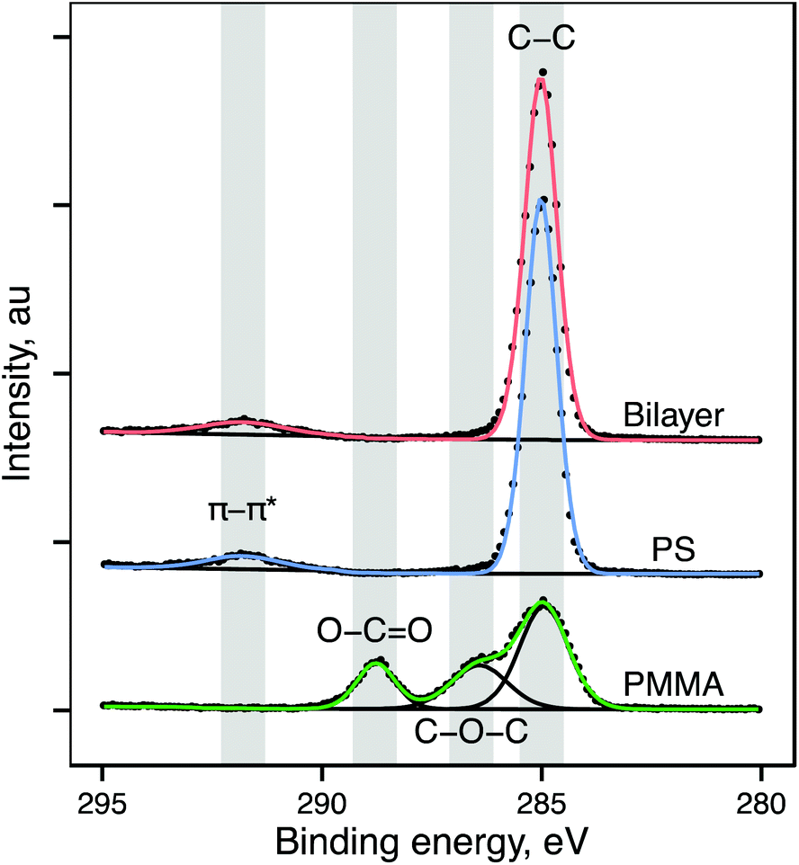 | ||
| Fig. 1 Representative high-resolution XPS scans of the C1s region for PMMA (bottom), polystyrene (center) and bilayer (top) spun-cast polymer films on Si wafer. Presence of the π–π* shakeup peak and absence of C–O–C and O–CO peaks (fitted components shown in black) in bilayer sample suggests the presence of an intact polystyrene overlayer atop initially deposited PMMA film. | ||
O components of the C1s region for PMMA, polystyrene and bilayer spun-cast polymer films. Values represent mean ± 1 standard deviation, n = 3. NR represents no measured peak for that component
| A | Atom percentages from survey scan | ||
|---|---|---|---|
| PMMA | Polystyrene | Bilayer | |
| Carbon | 72.0 ± 0.8 | 99.1 ± 1.0 | 99.9 ± 0.7 |
| Oxygen | 28.0 ± 0.8 | 0.9 ± 1.0 | 0.1 ± 0.7 |
| B | Area percentages from C1s components | ||
|---|---|---|---|
| PMMA | Polystyrene | Bilayer | |
| C–C | 54.9 ± 0.1 | 94.7 ± 0.6 | 94.7 ± 0.6 |
| C–O | 26.7 ± 0.4 | NR | NR |
| CO |
18.4 ± 0.5 | NR | NR |
| π–π* | NR | 5.3 ± 0.6 | 5.3 ± 0.6 |
Determination of sputter rates
To define an accurate sputter rate, the sputter time or dose through a known thickness of material is required. Table 2 shows measured film thicknesses and sputter times to the polymer–substrate interface, along with the calculated sputter rates, for single component polystyrene and PMMA films. Thicknesses of single component and bilayer films were measured by AFM profiling of a trench cut in the film by a scalpel blade. AFM was chosen as it allows direct measurement of film thickness. Polystyrene single component films have a mean thickness of 114 nm ± 7 nm (mean ± SD) and are slightly thicker than the PMMA single component films, which have a mean thickness of 105 ± 9 nm. Within experimental error, the sum of single component film thicknesses (220 nm) is not significantly different from the measured bilayer film thickness (223 nm), suggesting minimal interfacial mixing prior to depth profiling.| Film type | Thickness, nm | Sputter time to Si interface, s | Sputter rate, nm s−1 | Sputter yield, nm3 per atom |
|---|---|---|---|---|
| PMMA | 105 ± 5 | 22.4 ± 0.2 | 4.69 ± 0.24 | 0.108 ± 0.006 |
| Polystyrene | 114 ± 7 | 48.3 ± 1.6 | 2.37 ± 0.16 | 0.055 ± 0.004 |
| Bilayer | 223 ± 9 | 69.0 ± 0.1 | 3.23 ± 0.13 | 0.075 ± 0.003 |
From single-component films we see that PMMA sputters 1.97 times faster than polystyrene with sputter rates of 4.69 nm s−1 (PMMA) and 2.37 nm s−1 (polystyrene), respectively. These sputter rates may be converted to sputter yields of 0.108 nm3 per atom (PMMA) and 0.055 nm3 per atom (polystyrene) respectively, which are closely comparable to literature reported yields for argon clusters of same energy per atom.26–28 The difference between polystyrene and PMMA sputter rates compares favorably with reported sputter yields for the same polymers, using argon clusters of same energy per atom, in which the sputter yield of PMMA is 2.2 times that of polystyrene.9 It is important to note that the way in which sputtering rate decreases with sputter ion energy will vary between materials and is a function of variables including primary ion beam type, cluster size and energy.9,10,27,29
Depth profile of representative bilayer
Fig. 2A shows a representative ToF-SIMS depth profile through a polystyrene–PMMA bilayer. The intensities of characteristic ions for each layer (polystyrene: C7H7+, m/z 91; PMMA: C4H5O+, m/z 69; silicon: Si+, m/z 28) are plotted on a log10 scale against sputter time. Within the initial polystyrene layer the intensity of C7H7+ is stable. Between approximately 45 and 55 seconds of sputtering time the intensity of C7H7+ falls while that of C4H5O+ rises as the profile crosses the polystyrene–PMMA interface. In the underlying PMMA layer the intensity of C4H5O+ stabilizes. However, the intensity of C7H7+ does not fall to zero, but rather stabilizes at a lower intensity. This is due to the fact that m/z 91.05 is a minor peak in the PMMA spectrum. Additionally a small increase in the intensity of Si+ is seen at the polystyrene–PMMA interface, likely due to polydimethylsiloxane (PDMS) contamination of the PMMA stock solution. This hypothesis is supported by the appearance of characteristic PDMS peaks including SiC3H9+ and Si2C5H15O+ in the spectra of PMMA films (data not shown). Beyond 70 seconds of sputter time the polymer–silicon interface is seen as a rapid drop in intensity of C4H5O+ and C7H7+, corresponding with a significant rise of the Si+ peak. Beyond ∼75 seconds of sputter time the Si+ intensity stabilizes and the intensities of characteristic polymer peaks continue to fall in intensity. Throughout the depth profiles, no pinholes or defects were observed in ion images (data not shown), suggesting that films are intact and laterally homogeneous.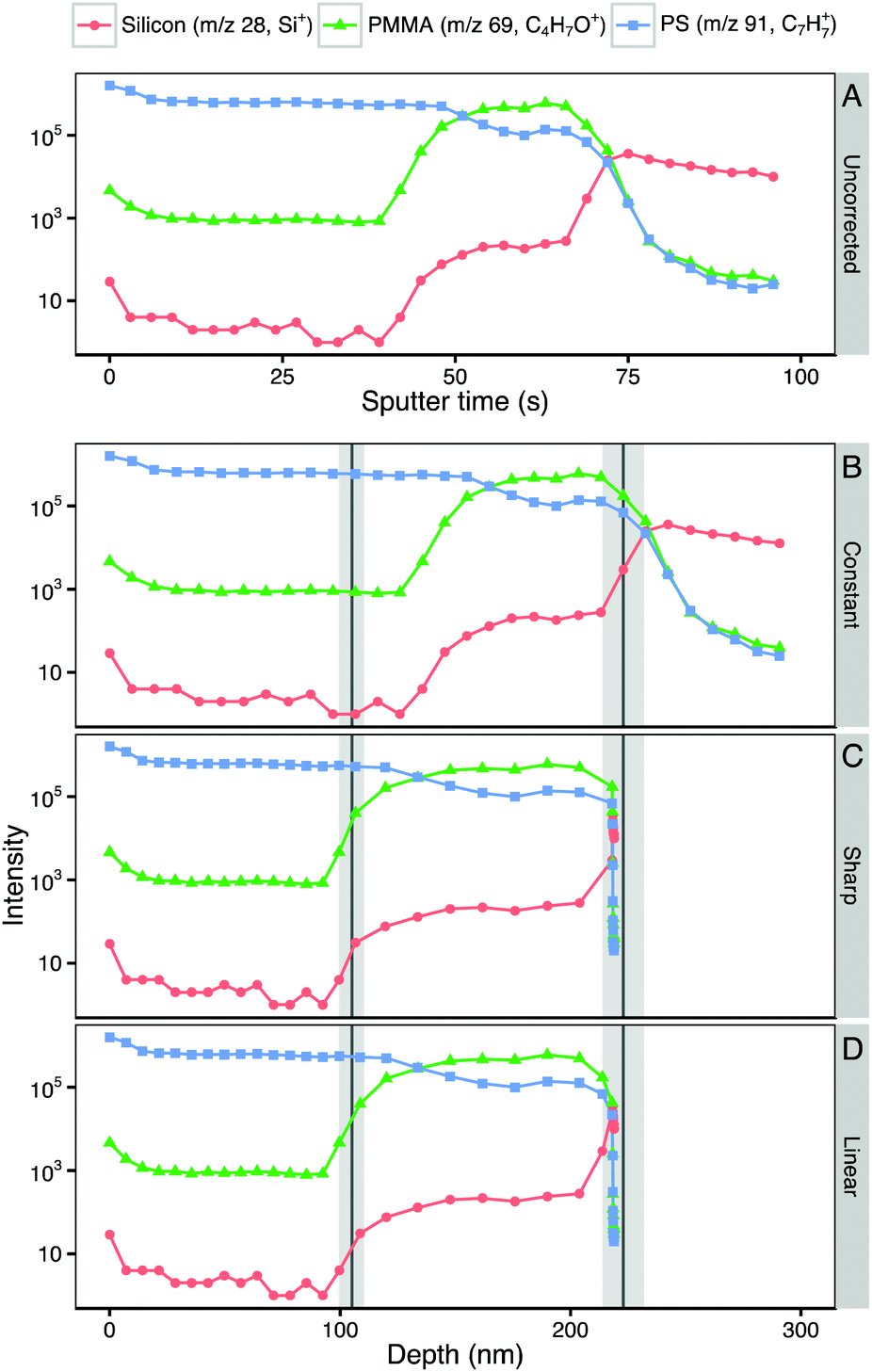 | ||
| Fig. 2 (A) Representative ToF-SIMS depth profile through a polystyrene–PMMA bilayer spun-cast film on Si wafer plotted against sputter time. (B–D) The same representative ToF-SIMS depth profile transformed to plot depth using different sputter rate assignment methods. (B) Transformation by constant sputter rate defined from measured bilayer thickness and sputter time to polymer–Si interface. (C) Transformation using step change between measured component sputter rates at polystyrene–PMMA and PMMA–Si interfaces. (D) Linear transition between component sputter rates across depth-resolution of polystyrene–PMMA and PMMA–Si interfaces. Intensities of characteristic peaks of each component (silicon: Si+, m/z 28; PMMA: C4H5O+, m/z 69; polystyrene: C7H7+, m/z 91) are plotted on a log10 intensity scale against sputter time (a) or depth from surface (b–d). Expected position of polystyrene–PMMA and PMMA–Si interfaces from AFM measurements of single-component and bilayer films are shown as vertical line (mean) and shaded area (±1 SD). | ||
In many cases it is sufficient to interpret depth profiles when plotted on their original axis of sputter time or ion dose. These include systems where components sputter at similar rates and where interfaces positions are tightly controlled by processing variables or otherwise already known.4 However, untransformed depth profiles only provide relative information on the position of features. Since in most experimental systems the locations of interfaces is not known, a translation to a depth scale is required to determine their position and size. To translate to a depth scale it is necessary to determine the sputter times at which polymer–polymer and polymer–substrate interfaces are seen. In this study we examined the first derivative of the intensity of the characteristic ion of the underlying layer (C4H5O+ for the polystyrene–PMMA interface and Si+ for the PMMA–silicon interface) to determine interface locations. It was found that identifying the position of the peak in the first derivative near an interface facilitates reproducible identification of interfacial sputter times. The peak maximum of the first derivative identifies the center of the interface and the full width at half maximum (FWHM) the interfacial width. Table 3 shows the sputter time to the polymer–polymer and polymer–substrate interfaces along with the interface widths measured using this method.
| PS–PMMA | PMMA–Si | ||||
|---|---|---|---|---|---|
| Transformation | Depth | Width | Depth | Width | |
| Time, s | N/A | 45.5 | 8.8 | 69.0 | 7.3 |
| Distance, nm | Constant | 147 | 28.5 | 223 | 23.6 |
| Step | 113 | 31.6 | 218 | 17.5 | |
| Linear | 113 | 31.1 | 218 | 17.3 | |
Transformation to depth scale
Having defined interfacial positions in sputter time, it is possible to compare methods of converting sputter time to depth. Fig. 2B–D show the results of three different transformations from sputter time to depth of the representative bilayer depth profile shown in Fig. 2A. The expected position of the polystyrene–PMMA and PMMA–silicon interfaces, based on measured film thickness, is marked by vertical lines (mean) and shaded areas (±1 standard deviation). Each of the three transformation methods are discussed below.As the measured depth of the polymer–Si interface is used to define the constant sputter rate, this transformation places the PMMA–silicon interface at exactly at the expected interface position of 223 nm. The polystyrene–PMMA interface is predicted to be at 147 nm, 33 nm deeper than the mean measured thickness of the polystyrene film. This difference in the interface position results in significantly different relative layer thicknesses for polystyrene and PMMA than expected. If the expected interface position was not known, and different sputter rates not considered, this incorrect depth scale could lead to erroneous conclusions as to the thickness of each layer and the locations of the layer interfaces (Table 4).
| Transformation method | |||||
|---|---|---|---|---|---|
| Constant | Step | Linear | AFM | ||
| Relative layer thickness | Polystyrene | 66.0% | 50.5% | 51.7% | 52.1% |
| PMMA | 34.0% | 49.6% | 48.3% | 47.9% | |
With a step-change between sputter rates in each layer of the film, the predicted polystyrene–PMMA interface position of 113 nm is more closely in line with the expected polystyrene overlayer film thickness of 114 ± 7 nm. The predicted depth of the PMMA–silicon interface (218 nm) is within one standard deviation of the expected overall bilayer film thickness (223 ± 9 nm). This results in apparent layer thicknesses closer to that expected from the measured film thicknesses, and a more accurate profile.
We hypothesized that the depth profile transformation may be further improved by interpolating the transition rate across interfaces. While others have accounted for this region using the relative intensity of characteristic ions for each layer,16 sputtering behavior may not follow relative ion intensity. To assess how the sputter rate transition across the polymer–polymer interface should be modeled, spun cast films of polystyrene–PMMA blends were prepared from toluene. Quantification of XPS spectra of blended polymer films (Fig. 3A) shows a linear decrease in the intensity of the C1s peak (285 eV), and π–π* shakeup peak (290 eV), and linear increase of the CO and O1s peaks, as PMMA content is increased in polystyrene–PMMA blends, indicating that blends were well mixed. Film thicknesses of blended polymer films were measured by AFM profiling of scalpel-cut trenches. Films were depth profiled as described for single component films, and sputter rates determined relative to pure polystyrene (Fig. 3B). With increasing polystyrene content an approximately linear decreasing trend in relative sputter rate is observed. Therefore, to further improve the model, we allow the sputter rate to change linearly between known single component sputter rates across the interfacial width. In other systems it may be more appropriate to apply another function to model sputter rate transition: Power-law, exponential or other functions may all be easily applied. These may be applicable where a component with low sputter rate as a single component exhibits a greatly enhanced sputtering in the presence of another component. These effects have been observed in the sputter characteristics of some drug doped polymer materials. For example, Mahoney et al. (2005) noted that pluronic-P104 sputtered much more efficiently as a triblock copolymer with PLLA than as a single component material.33
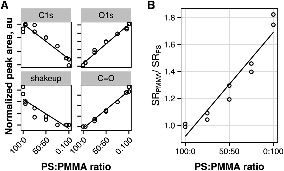 | ||
| Fig. 3 Characterization of polystyrene–PMMA blend films. (A) XPS peak intensities for blends. (B) Sputter rates of blends relative to pure polystyrene. Linear trend lines shown. | ||
The PMMA–Si interface appears at 218 nm, in line with that predicted by the step-change transformation, and within one standard deviation of the expected overall bilayer film thickness (223 ± 9 nm). Fig. 4 shows the polymer–Si interfacial region of reconstructed depth profiles in more detail. In the step-change reconstruction peak intensities are seen to abruptly change at the interface. Modeling a linear transition in sputter rate yields a smoother shape to the interface, and more closely reflects the expected differences in sputter rate and component mixing between each sputter-roughened analysis slice within the interfacial region.34
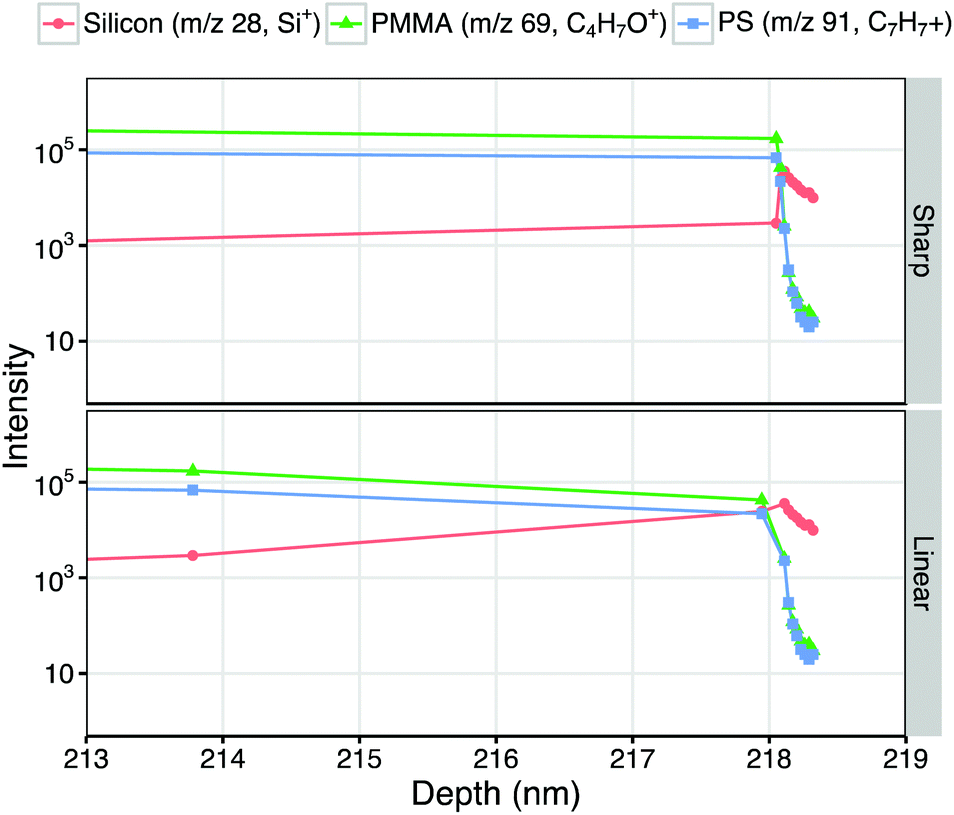 | ||
| Fig. 4 Enlargements from Fig. 2, showing the polymer–Si interface regions of representative depth profiles reconstructed with sharp (top) and linear (bottom) sputter rate transitions. Intensities of characteristic peaks of each component (silicon: Si+, m/z 28; PMMA: C4H5O+, m/z 69; polystyrene: C7H7+, m/z 91) are plotted on a log10 intensity scale against depth from surface. | ||
![[thin space (1/6-em)]](https://www.rsc.org/images/entities/char_2009.gif) :50 blend. Fig. 5A shows representative AFM height images of film surfaces before sputtering and crater bases after 3, 9 or 15 seconds of sputtering. Fig. 5B shows the roughness (Rq) of film surfaces and crater bases, calculated from representative AFM images. Horizontal line scans across representative AFM images can be found in the ESI.† At the film surface, the blended film exhibits raised domains ∼250 nm across and ∼10 nm high, indicative of phase separation-induced topography. While phase separation was not promoted by an annealing step, these features are of comparable scale to those previously described for polystyrene–PMMA systems,35,36 although they may not directly correspond to chemical phase-separations.37 Such features are not seen at the surface of either pure film, which appear flat (Rq < 1 nm) and uniform.
:50 blend. Fig. 5A shows representative AFM height images of film surfaces before sputtering and crater bases after 3, 9 or 15 seconds of sputtering. Fig. 5B shows the roughness (Rq) of film surfaces and crater bases, calculated from representative AFM images. Horizontal line scans across representative AFM images can be found in the ESI.† At the film surface, the blended film exhibits raised domains ∼250 nm across and ∼10 nm high, indicative of phase separation-induced topography. While phase separation was not promoted by an annealing step, these features are of comparable scale to those previously described for polystyrene–PMMA systems,35,36 although they may not directly correspond to chemical phase-separations.37 Such features are not seen at the surface of either pure film, which appear flat (Rq < 1 nm) and uniform.
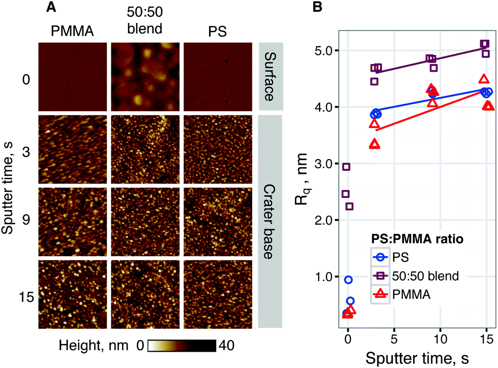 | ||
| Fig. 5 (A) Representative AFM height maps of PS, PMMA and blended films and crater bases after sputtering for 0 (surface), 3, 9, or 15 (crater bottom) seconds. Images show 1 × 1 μm area. (B) Roughness parameter (Rq) of film surface and sputter crater bases in PS, PMMA and blended films. Linear trend fitted for 5–15 s of sputter time. | ||
For all films, the roughness of crater base was substantially higher than for the film surface. Roughness was seen to increase with sputter time. It was seen that the roughness of blended films was significantly higher than for pure films at all sputter times. It was noted that the lateral feature size of the topography after sputtering was smaller than the phase-separated domains seen at the film surface for the 50/50 blend. These results suggest that surface features caused by polymer phase separation are quickly removed by sputter-induced roughening of short lateral feature size and ∼10 nm depth range. The phase separation seen here is not expected to adversely influence ToF-SIMS data interpretation, particularly given a ∼25-fold difference between the roughness length-scale of crater bases and the SIMS analysis area. No significant difference in polymer–Si interface width was observed for depth profiles of blended polymers.
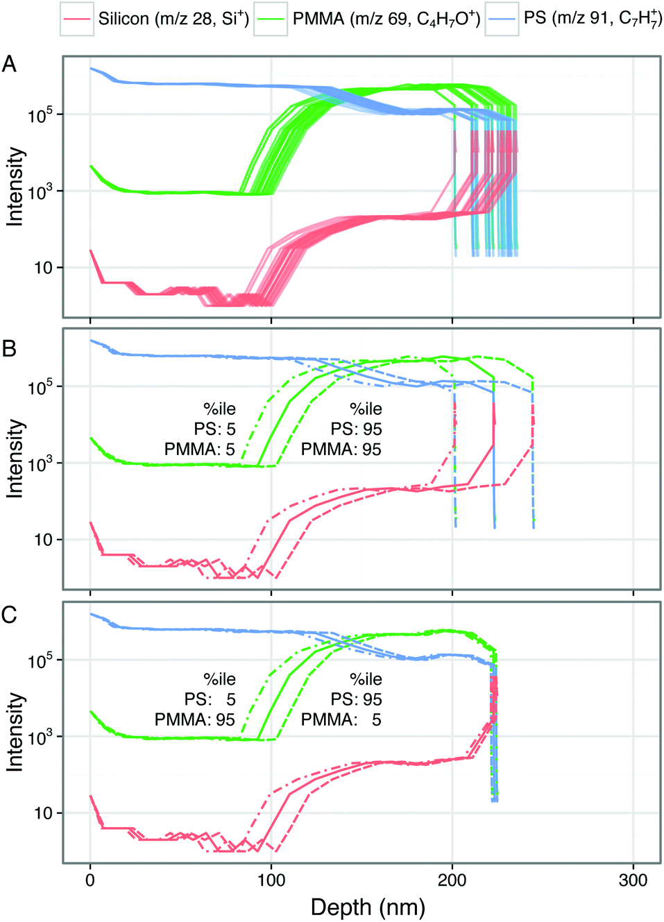 | ||
| Fig. 6 (A) Depth profiles (n = 20) reconstructed from simulated sputter rates, normally distributed around the mean of the measured sputter rates. (B) Depth profiles reconstructed with sputter rates selected from the 5th (dashed line) or 95th (dot-dashed line) percentile of sputter rates for both polystyrene and PMMA. (C). Depth profiles reconstructed with sputter rates selected from the 5th and 95th percentile (dot-dashed line), or 95th and 5th percentile (dashed line) for polystyrene and PMMA respectively. Profiles reconstructed from mean sputter rates is shown with a solid line. | ||
In Fig. 6B and C we highlight specific cases of erroneous reconstructions that may arise from the combination of errors in each component sputter rate. When sputter rates are sampled from the same percentile of a normal distribution derived from the mean and standard deviation of calculated sputter rates, errors are introduced both in interface position and layer thickness. Selecting sputter rates from the 5th percentile (slower sputter rate than mean) for both polystyrene and PMMA gives apparent polymer–polymer and polymer–Si interfaces shallower than for mean sputter rates (Fig. 6B). When both are selected from the 95th percentile (faster sputter rate than mean) this is reversed, with interface positions deeper than for mean sputter rates. These deviations are ±12 nm for the polymer–polymer interface, and ±22 nm for the polymer–silicon interface. When sputter rates from polystyrene and PMMA samples were selected from percentiles on opposite tails of their respective distribution (5th and 95th, or 95th and 5th), reconstructions place the polymer–Si interface close to that for mean values as the errors in sputter rates cancel one another out (Fig. 6C). However, they continue to displace the apparent polymer–polymer interface position by up to ±12 nm. These scenarios help visualize how errors in the determination of multiple sputter rates mix to produce transformed depth profiles that may not reflect the chemical distribution or thickness of the sample. These results demonstrate the necessity of accurately assigning component sputter rates and validating transformed profiles against expected sample thickness and interface positions. They additionally highlight the potential impact of errors in their determination on reconstructed depth profiles.
Future challenges
Several studies have considered depth profiling and 3D reconstruction of drug-eluting polymer stents.2,3 In these studies depth scales were assigned using single sputter rates, despite evidence of both drug-polymer phase separation and different sputter rates with drug loading. This represents a scenario where consideration of differences in sputtering may be advantageous. Accurate sputter rate determination is essential for accurate depth profile and 3D reconstruction. In order to account for sputter rate behavior within interfaces, further fundamental studies of blended materials and phase-separated interfaces are required. Different sputter rates may also be expected in biological materials. For sample, mammalian cells have been broadly seen to sputter at the same rate across membrane, cytoplasm and nucleus,30,38,39 while plant tissues have previously been shown to exhibit different sputter rates between cellular components.40 Future studies investigating the interface of cells and polymeric scaffolds used for tissue engineering will certainly require consideration of multiple sputter rates.This study has considered the reconstruction of one-dimensional depth profiles along the z-axis. Correcting for sputter rate differences in 3D ToF-SIMS is a significantly greater challenge. Simple 3D corrections may in the future be accomplished by voxel-stretching, however, an ideal correction would likely need to create new voxels containing reconstructed spectra. Accurate depth profile reconstruction of industrially and clinically relevant, multicomponent, organic and biological systems will require careful and considered application of many factors including correction for sputter rate effects addressed in this study.
Experimental
Preparation of polymer films
10 cm diameter silicon wafers (Silicon Valley Microelectronics, CA) were scored and diced into 1 × 1 cm squares. Silicon squares were cleaned by sequential sonication in ultra-pure, deionized water, dichloromethane, acetone and methanol, with two 15 min washes for each solvent, and allowed to dry before use. Solutions of 30000 MW polystyrene and 15000 MW PMMA (both Scientific Polymer Products Inc.), and 25:75, 50:50 or 75:25 mass ratio blends of these, were prepared by dissolving 3% wt:volume of polymer in toluene (PMMA and polystyrene/PMMA blends) or 1-chloropentane (pure polystyrene only) with sonication.
:vol solution in toluene on Si wafer as above. After drying overnight under vacuum to ensure complete solvent evaporation, a polystyrene overlayer was spun cast from a 3% wt:vol solution in 1-chloropenane atop the PMMA film using the same parameters.
Film thickness measurement
Thickness of polymer films was measured by AFM profiling. Trenches were prepared in polymer films by scoring with the back of a scalpel blade. At least n = 3 trenches per film type were profiled using a Dimension Icon-PT AFM (Bruker). The instrument was operated in ScanAsyst mode using ScanAsyst-Air tips (Bruker) with a resonant frequency of 50–90 kHz and a force constant of 0.4 N m−1. Height images were collected across a 90 μm × 90 μm area with scan rate of 0.6 Hz and 256 samples per line. Images were analyzed using NanoScope Analysis v1.5 (Bruker). Representative images (n = 3) were flattened using a 1st order algorithm, pre-selecting areas known to represent the film surface. Trench depth was measured using the step measurement tool.Crater roughness measurement
The roughness of sputter craters produced in spun-cast films of polystyrene, PMMA, or a 50:50 blend, was determined by tapping-mode AFM. Craters measuring 600 × 600 μm were produced in polymer films by sputtering using the parameters described for ToF-SIMS data collection below for 3, 9 or 15 seconds. Crater bottoms and original polymer surfaces were analyzed using a Dimension Icon-PT AFM (Bruker). The instrument was operated in tapping mode using Tap300Al-G tips (Budget Sensors) with a resonant frequency of 300 kHz and a force constant of 40 N m−1. Height images were collected across a 1 × 1 μm area with a scan rate of 1 Hz and 256 samples per line. Images were analyzed using NanoScope Analysis v1.5 (Bruker). Representative images (n = 4) were flattened using a 1st order algorithm, and roughness (Rq) calculated across the whole image area, excluding any notable artifacts. Horizontal line scans were reconstructed from row 128 of the representative images.
XPS analysis
XPS spectra were obtained from representative bilayer and single-component and blended films (n = 2 for each sample) using a Kratos AXIS Ultra DLD (Kratos, Manchester, UK) instrument in the “hybrid” mode (large photoelectron acceptance angle) using a monochromatic Al Kα X-ray source and a nominal photoelectron takeoff angle 0°. Survey scans were collected between 0–1200 eV binding energy for two spots per sample with an 80 eV pass energy and 1 eV step-size. High-resolution scans of the C1s region were acquired with a 20 eV pass energy and 0.1 eV step-size. A low-energy flood gun was used for charge neutralization. XPS data was plotted and analyzed in CasaXPS v2.3 (Casa Software Ltd). All binding energies are referenced to the C1s hydrocarbon peak at 285 eV.ToF-SIMS data collection
ToF-SIMS depth profiling was performed using an ION-TOF TOF SIMS 5–100 (ION-TOF GmbH, Münster, Germany) instrument equipped with a Bin+ liquid metal ion gun (LMIG) source and an Arn+ gas cluster ion bombardment (GCIB) source. Both sources were arranged with a 45° angle of incidence with respect to the substrate, and rotated 180° around the z-axis with respect to each other. The analysis chamber was maintained at less than 1 × 10⁻⁸ mbar. The instrument was operated in a dual-beam, non-interlaced mode with sequential cycles of analysis and sputtering. 25 keV Bi3+ clusters were used for analysis and 10 keV Ar1000+ clusters were used for sputtering. An electron flood gun was used to neutralize charge build-up following sputter and analysis cycles. The target current of the analysis beam was maintained at 0.05 pA. The target current of the sputter source was maintained at 2.5 nA. Positive ion depth profiles were acquired using a dose of 2.9 × 10¹¹ ions per cm2 per analysis cycle from a 100 × 100 μm area at a 256 × 256 pixel density. Sputtering was carried out for 3 seconds over a 600 × 600 μm area for a dose of 1.3 × 10¹³ ions per cm2 per sputter cycle, followed by a 0.5 second pause for charge neutralization. This analysis/sputter cycle was repeated until the intensity of a secondary ion characteristic of the silicon substrate (Si+) was seen to stabilize, indicating completion of depth profiling through the film. Positive secondary ion spectra were mass calibrated to the CH+, CH2+ and C2H3+ peaks. Mass resolution at the C2H3+ peak (m/z 27) was typically above 6000. Peaks in the positive ion spectra at m/z 28 (Si+), 69 (C4H5O+) and 91 (C7H7+), were identified as characteristic peaks of the Silicon substrate, PMMA, and polystyrene respectively. Depth profile data for these peaks were exported as tab separated files for plotting and transformation to a depth scale in RStudio v0.98 (RStudio Inc).Determination of interface position
The sputter time to polymer–polymer and polymer–silicon interfaces were determined from the first derivative of the log10 transformed intensity of the characteristic peak of the underlying layer. The location of the maxima nearest the interface position defines the time to the interface. The width of the interface was defined as the full width at half maximum (FWHM) of this peak within the first derivative. If the peak seen in the first derivative is assumed to be Gaussian, which provides a good fit, the boundaries of the FWHM are the time points at which the intensity reaches the commonly used 16% and 84% intensity values used to characterize interfaces.11 This allows for semi-automated and unbiased interface determination relatively free of subjective operator errors. Both the depth profile and first derivative were fit using LOESS smoothing functions, and intensities predicted in a step-wise fashion using RStudio.Determining component sputter rates
Component sputter rates for polystyrene and PMMA and polymer blends were calculated using single-component films. Film thicknesses measured by AFM (n = 3) was divided by sputter time to polymer–Si interfaces determined from depth profiles (n = 3). The average sputter rate across bilayer films was determined using the same procedure. While others have observed sputter yields up to 0.01 nm3 per atom with 10 eV per atom argon clusters,27 we observed no resulting sputter crater from extensive sputtering of the uncoated silicon substrate. Therefore, we assumed a sputter rate of silicon as 0.03 nm s−1 (∼0.001 nm3 per atom at 10 eV per atom), approximately two orders of magnitude lower than that of polystyrene or PMMA, and in line with previously reported sputter rates for silicon with a C60 primary ion ranging from 0.01–0.1 nm s−1.15,41 Molecular dynamic simulations of Arn+ cluster impacts with bare silicon predict similarly low sputter yields at 10 eV per atom.42Depth profile reconstruction
Plotting and depth profile transformation was performed in RStudio. Depth transformations were performed in a step-wise fashion. For step-change and linear transformations interface positions were determined as described above.Conclusions
Many studies have investigated challenges in sputter depth profiling multicomponent systems using ToF-SIMS including depth resolution, sputter induced damage, and the ability to sputter through a wide range of materials. However, relatively few have addressed correcting for components with different sputter rates through the profile. Using spun-cast bilayer samples of polystyrene and PMMA, this study has shown the following: (1) where the depth profile is transformed to a depth scale using a single constant sputter rate, apparent layer thicknesses do not match expected values, with the predicted polymer–polymer interface shifted ∼33 nm deeper than expected (14% of total film thickness). This is due to the fact that the different sputter rates of the components were not accounted for. (2) Accounting for changes in sputter rate with a step-change between known single-component sputter rates provides layer thickness and interface positions in line with measured values. (3) Instantaneous sputter rate transition across an interface is unrealistic, and polystyrene–PMMA blends exhibit a linear increase in sputter rate with increasing PMMA content. (4) Applying a linear transition between component sputter rates across the interface width may yield a profile shape that more closely recapitulates expected sputtering phenomena when sufficient data points are collected across the interfacial width. (5) Accurate determination of sputter rates is critical to producing accurately reconstructed depth profiles. This study provides an easily implemented methodology for the translation of sputter time or ion dose to depth in depth profiles, yielding accurate interface positions and apparent layer thicknesses in scenarios where differences in sputter rates between components may otherwise provide erroneous or misleading results. It is possible that this methodology could be applied to the accurate reconstruction of 3D images of systems exhibiting differences in component sputtering behavior.Acknowledgements
We gratefully acknowledge support of the research by NIH grant EB-002027 to NESAC/BIO, and thank Gerry Hammer for collection of XPS spectra.References
- T. Mouhib, C. Poleunis, N. Wehbe, J. J. Michels, Y. Galagan, L. Houssiau, P. Bertrand and A. Delcorte, Analyst, 2013, 138, 6801–6810 RSC.
- C. M. Mahoney, A. J. Fahey and A. M. Belu, Anal. Chem., 2008, 80, 624–632 CrossRef CAS PubMed.
- G. L. Fisher, A. M. Belu, C. M. Mahoney, K. Wormuth and N. Sanada, J. Proteome Res., 2009, 81, 9930–9940 CAS.
- A. G. Shard, R. Havelund, M. P. Seah, S. J. Spencer, I. S. Gilmore, N. Winograd, D. Mao, T. Miyayama, E. Niehuis, D. Rading and R. Moellers, Anal. Chem., 2012, 84, 7865–7873 CrossRef CAS PubMed.
- J. Bailey, R. Havelund, P. Dubruel, A. G. Shard, I. S. Gilmore, M. R. Alexander and D. J. Scurr, ACS Appl. Mater. Interfaces, 2015, 7, 150106143135007–2659 Search PubMed.
- N. Wehbe, T. Tabarrant, J. Brison, T. Mouhib, A. Delcorte, P. Bertrand, R. Moellers, E. Niehuis and L. Houssiau, Surf. Interface Anal., 2012, 45, 178–180 CrossRef PubMed.
- C. Bich, R. Havelund, R. Moellers, D. Touboul, F. Kollmer, E. Niehuis, I. S. Gilmore and A. Brunelle, J. Proteome Res., 2013, 85, 7745–7752 CAS.
- S. Rabbani, A. M. Barber, J. S. Fletcher, N. P. Lockyer and J. C. Vickerman, J. Proteome Res., 2011, 83, 3793–3800 CAS.
- P. J. Cumpson, J. F. Portoles and N. Sano, J. Vac. Sci. Technol., A, 2013, 31, 020605 Search PubMed.
- P. J. Cumpson, J. F. Portoles, A. J. Barlow and N. Sano, J. Appl. Phys., 2013, 114, 124313 CrossRef PubMed.
- E.42 Committee, Standard Guide for Measuring Widths of Interfaces in Sputter Depth Profiling Using SIMS, ASTM International, West Conshohocken, PA, 2011 Search PubMed.
- S. Hofmann, Surf. Interface Anal., 2003, 35, 556–563 CrossRef CAS PubMed.
- S. Hofmann, J. Erlewein and A. Zalar, Thin Solid Films, 1977, 43, 275–283 CrossRef CAS.
- S. Hofmann, J. Vac. Sci. Technol., A, 1998, 16, 1096 CAS.
- A. Wucher, J. Cheng and N. Winograd, Anal. Chem., 2007, 79, 5529–5539 CrossRef CAS PubMed.
- M. S. Wagner, Anal. Chem., 2004, 76, 1264–1272 CrossRef CAS PubMed.
- S. Muramoto, J. Brison and D. G. Castner, Surf. Interface Anal., 2010, 43, 58–61 CrossRef PubMed.
- A. Wucher and H. Oechsner, Z. Anal. Chem., 1989, 333, 470–473 CrossRef CAS.
- A. Wucher, J. Cheng and N. Winograd, Appl. Surf. Sci., 2008, 255, 959–961 CrossRef CAS PubMed.
- A. Wucher and H. Oechsner, Z. Anal. Chem., 1989, 333, 470–473 CrossRef CAS.
- W. K. Way, S. W. Rosencrance and N. Winograd, Surf. Sci., 1993, 2, 67–70 CAS.
- S. W. Rosencrance, W. K. Way and N. Winograd, Surf. Sci., 1993, 2, 71–75 CAS.
- A. Chilkoti, D. G. Castner and B. D. Ratner, Appl. Spectrosc., 1991, 45, 209–217 CrossRef CAS.
- G. P. López, D. G. Castner and B. D. Ratner, Surf. Interface Anal., 1991, 17, 267–272 CrossRef PubMed.
- D. Ennis, H. Betz and H. Ade, J. Polym. Sci., Part B: Polym. Phys., 2006, 44, 3234–3244 CrossRef CAS PubMed.
- P. J. Cumpson, J. F. Portoles, A. J. Barlow, N. Sano and M. Birch, Surf. Interface Anal., 2013, 45, 1859–1868 CrossRef CAS PubMed.
- M. P. Seah, J. Phys. Chem. C, 2013, 117, 12622–12632 CAS.
- V. Cristaudo, C. Poleunis, B. Czerwinski and A. Delcorte, Surf. Interface Anal., 2014, 46, 79–82 CrossRef CAS PubMed.
- K. Shen, A. Wucher and N. Winograd, J. Phys. Chem. C, 2015, 119, 15316–15324 CAS.
- J. Brison, D. S. W. Benoit, S. Muramoto, M. Robinson, P. S. Stayton and D. G. Castner, Surf. Interface Anal., 2010, 43, 354–357 CrossRef PubMed.
- J. Brison, M. A. Robinson, D. S. W. Benoit, S. Muramoto, P. S. Stayton and D. G. Castner, Anal. Chem., 2013, 85, 10869–10877 CrossRef CAS PubMed.
- N. Wehbe, T. Mouhib, A. Delcorte, P. Bertrand, R. Moellers, E. Niehuis and L. Houssiau, Anal. Bioanal. Chem., 2014, 406, 201–211 CrossRef CAS PubMed.
- C. M. Mahoney, J. Yu and J. A. Gardella, Anal. Chem., 2005, 77, 3570–3578 CrossRef CAS PubMed.
- D. Mao, A. Wucher and N. Winograd, Anal. Chem., 2009, 82, 57–60 CrossRef PubMed.
- L. Kailas, J.-N. Audinot, H.-N. Migeon and P. Bertrand, Appl. Surf. Sci., 2004, 231–232, 289–295 CrossRef CAS PubMed.
- L. Kailas, B. Nysten and P. Bertrand, Surf. Interface Anal., 2004, 36, 1227–1230 CrossRef CAS PubMed.
- C. Ton-That, A. G. Shard, D. O. H. Teare and R. H. Bradley, Polymer, 2001, 42, 1121–1129 CrossRef CAS.
- S. Chandra, W. A. Ausserer and G. H. Morrison, J. Microsc., 1987, 148, 223–229 CrossRef CAS PubMed.
- M. A. Robinson, D. J. Graham and D. G. Castner, Anal. Chem., 2012, 84, 4880–4885 CrossRef CAS PubMed.
- A. J. Patkin, S. Chandra and G. H. Morrison, Anal. Chem., 1982, 54, 2507–2510 CrossRef CAS.
- J. Cheng and N. Winograd, Anal. Chem., 2005, 77, 3651–3659 CrossRef CAS PubMed.
- N. A. Kubota, D. J. Economou and S. J. Plimpton, J. Appl. Phys., 1998, 83, 4055–4063 CrossRef CAS PubMed.
Footnote |
| † Electronic supplementary information (ESI) available. See DOI: 10.1039/c5an00860c |
| This journal is © The Royal Society of Chemistry 2015 |