
 Open Access Article
 This Open Access Article is licensed under a
 Creative Commons Attribution 3.0 Unported Licence
Application of scanning angle Raman spectroscopy for determining the location of buried polymer interfaces with tens of nanometer precision†
Craig A.
Damin‡
ab,
Vy H. T.
Nguyen‡
ab,
Auguste S.
Niyibizi
a and
Emily A.
Smith
*ab
aAmes Laboratory, U.S. Department of Energy, Ames, IA 50011-3111, USA. E-mail: esmith1@iastate.edu
bDepartment of Chemistry, Iowa State University, Ames, IA 50011-3111, USA
First published on 11th February 2015
Abstract
Near-infrared scanning angle (SA) Raman spectroscopy was utilized to determine the interface location in bilayer films (a stack of two polymer layers) of polystyrene (PS) and polycarbonate (PC). Finite-difference-time-domain (FDTD) calculations of the sum square electric field (SSEF) for films with total bilayer thicknesses of 1200–3600 nm were used to construct models for simultaneously measuring the film thickness and the location of the buried interface between the PS and PC layers. Samples with total thicknesses of 1320, 1890, 2300, and 2750 nm and varying PS/PC interface locations were analyzed using SA Raman spectroscopy. Comparing SA Raman spectroscopy and optical profilometry measurements, the average percent difference in the total bilayer thickness was 2.0% for films less than ∼2300 nm thick. The average percent difference in the thickness of the PS layer, which reflects the interface location, was 2.5% when the PS layer was less than ∼1800 nm. SA Raman spectroscopy has been shown to be a viable, non-destructive method capable of determining the total bilayer thickness and buried interface location for bilayer samples consisting of thin polymer films with comparable indices of refraction.
Introduction
Thin and ultrathin polymer films are currently employed for use in the fields of optics, photovoltaics, microelectronics, and coatings.1–3 In many applications, the thickness and composition of these films affect their function; therefore, accurate determinations of film thickness and composition are required. Interferometric methods, such as scanning white light interferometry, are commonly used to measure the thickness of polymer films.4–6 A 2008 study by Madani-Grasset et al. employed a commercial scanning white light interferometer to determine thickness and homogeneity of 3 to 15 nm thick films of PS deposited on a borosilicate glass substrate.7 Interferometry offers a fast, non-contact optical method capable of determining film thickness with high accuracy; however, this technique does not provide chemical information about the samples.Attenuated total (internal) reflection-Fourier transform infrared (ATR-FT-IR) spectroscopy is a viable technique for depth profiling thin polymer films.8,9 ATR-FT-IR spectroscopy is performed by placing the sample in optical contact with an internal reflection element.10–13 Infrared light passing through the internal reflection element at angles equal to or greater than the critical angle will undergo total internal reflection (TIR) at the interface, resulting in the formation of an evanescent wave in the sample. Depth profiling using ATR-FT-IR spectroscopy can be accomplished by varying the penetration depth of the evanescent wave, which is dependent on the wavelength and angle of incidence. The wavelength dependence of the penetration depth complicates the analysis since the penetration depth is not constant across the entire spectrum.
Confocal Raman spectroscopy utilizes a remote, limiting aperture placed at an image plane of the illuminated sample to reduce the contributions from out-of-focus regions and improve axial spatial resolution.14 Everall has shown the capabilities and limitations of performing z-axis scanning by confocal Raman spectroscopy for the analysis of multi-layered samples, such as polymers.15–18 Even though the axial spatial resolution can be improved through the use of a confocal aperture, the resolution is still on the order of a few hundreds of nanometers or more.
TIR-Raman (alternatively ATR-Raman) spectroscopy offers a potential solution to the problems associated with ATR-FT-IR spectroscopy and confocal Raman spectroscopy.19–21 TIR-Raman spectroscopy is analogous to ATR-FT-IR spectroscopy in that the sample must be optically coupled to a material possessing a high index of refraction. Distinct from ATR-FT-IR spectroscopy, the Raman excitation wavelength is fixed and an order of magnitude shorter resulting in a reduced penetration depth of the evanescent wave, a value that is constant across the entire spectrum. The capability of TIR-Raman spectroscopy for characterizing thin surface layers was studied by Iwamoto et al. using a bilayer of polystyrene (PS) with polyethylene or polycarbonate (PC).22 They reported that Raman spectra could be collected from PS surface layers as thin as 0.006–0.2 μm and that the thickness of the film could be determined by varying the incident angle of the laser excitation. A 2004 study by Tisinger and Sommer represented the first attempt at performing TIR-Raman spectroscopy using a conventional Raman microscope.23 The authors reported Raman spectra of a 3.2 μm thick polydiacetylene film spin coated onto the bottom of a zinc selenide prism. Thickness measurements of thin isotropic PS films on polypropylene substrates were performed by Kivioja et al. using TIR-Raman spectroscopy.24
Scanning angle (SA) Raman spectroscopy (alternatively known as variable angle Raman spectroscopy) is similar to TIR-Raman spectroscopy in that both techniques utilize similar sample geometries. However, unlike TIR-Raman spectroscopy, in which the angle of incidence at the prism-sample interface is usually fixed and equal to or greater than the critical angle required for TIR, SA Raman spectroscopy is performed by scanning the incidence of the laser excitation over a range of angles while collecting the Raman scattered light. SA Raman spectroscopy is suited to measuring optical waveguides possessing thicknesses on the order of the excitation wavelength. Radiative, or “leaky”, waveguides can occur at the prism-dielectric film interface when ηprism > ηlayer 1 > ηlayer 2 (η represents the index of refraction).25 The optical energy density localized to the waveguide film can exhibit an interference pattern across selected incident angles due to multiple total internal reflections within the film.26 Enhancements in the optical energy density are observed at angles where constructive interference occurs. Among other parameters, these enhancements are dependent upon the thickness of the dielectric film.
A study by Levy et al. indicated that thin films supported on a substrate forming an asymmetric slab waveguide could be used to obtain a Raman spectrum.26 Waveguide Raman spectroscopy was later used to study ultrathin polymer films by Rabolt et al.27–30 Optical waveguide modes in thin polymer films were also studied by Miller and Bohn.31–35 Miller et al. compared the experimentally observed Raman scattering ratios of PS and poly(vinylpyrrolidone) to those based on computational iterations of film thicknesses and indices of refraction.32 It was concluded that such calculations for a range of waveguide thicknesses would require extensive computational time and a more efficient method capable of relating the electric field intensities to the observed Raman signals of multi-layered samples with varying thicknesses was needed.
Fontaine and Furtak demonstrated the extraction of depth-resolved vibrational information from transparent, optically homogeneous samples, including a 15 μm PS film using SA Raman spectroscopy.36 They later demonstrated the ability to determine the thickness of a single-layer PS film and the location of buried interfaces between two immiscible polymers, PS and poly(methyl methacrylate) (PMMA).25 The thicknesses of the single-layer PS films and the PS/PMMA bilayer were determined using the integrated scattering intensities of PS and PMMA Raman transitions. Although film thicknesses and the buried interface location were determined, the study was limited to a single 1200 nm PS film and a 3045 nm PS/PMMA bilayer sample. The model presented by Fontaine and Furtak could not be easily applied to other samples.
In a 2008 publication by Ishizaki and Kim, a near-infrared TIR-Raman spectrometer capable of measuring polymer surfaces was reported.37 The utility of the instrument was demonstrated by collecting Raman spectra from a bilayer film consisting of a 130 nm thick layer of PS and a 250 μm thick layer of poly(vinyl methylether) at various incident angles between 50 and 70°. Ishizaki and Kim demonstrated the incident angle dependency of the Raman intensities for the PS/poly(vinyl methylether) sample and calculated the optical electric field at the prism/PS interface; however, the study did not include a method of determining the thicknesses of the films and the location of the buried interface between the polymers.
In 2010, McKee and Smith discussed the development of a SA Raman spectrometer capable of precisely varying the angle of incidence for measuring interfacial phenomena with chemical specificity and high axial resolution.38 Meyer et al. presented a SA Raman method for measuring the thickness and composition of PS films spin coated onto a sapphire substrate using this instrument.39 The goals of the present study were to present reliable models for determining: (1) the total thickness of PS/PC bilayer films and (2) the location of the buried PS/PC interfaces using SA Raman spectroscopy. Calibration models based on the SSEFs were constructed and applied to experimental SA Raman spectroscopy data for PS/PC bilayer films with total thicknesses ranging from 1.3–2.8 μm with varying interface locations.
Experimental
Sample preparation
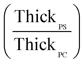
Polystyrene (PS, MW = 280 × 103) and poly(bisphenol A carbonate) (PC, MW = 64 × 103) were purchased from Sigma-Aldrich (St. Louis, MO). Solutions of PS in toluene and PC in methylene chloride were prepared with concentrations ranging from 0.02–0.14 g mL−1. Thin films of PS and PC were prepared using a Chemat Technology (Northridge, CA) KW-4A spin coater. First, 200 μL of the PS solution was dispensed onto a 25.4 mm diameter (0.5 mm thickness) sapphire disk (Meller Optics, Providence, RI). After depositing the solution, the substrate was spun at 3000 rpm for 60 seconds. The PS film was allowed to dry overnight at room temperature. Thin films of PC were prepared on BK7 glass slides (Corning Glass, Corning, NY) using the same method as that used for the PS films. The thicknesses of the PS and PC films were determined using a Zygo (Middlefield, CT) NewView 7100 3D optical surface profiler. Calibration curves of PS and PC film thickness, as measured by optical profilometry, versus the concentration of the polymer solution spin coated on the substrate are shown in ESI Fig. S1.†Bilayer films of PS and PC were prepared using the wedge transfer method.40 The thickness of the PS layer divided by the thickness of the PC layer was defined as ThickPS/ThickPC. The bilayer samples were prepared to represent the conditions of: (1) ThickPS/ThickPC < 1, (2) ThickPS/ThickPC ≈ 1, and (3) ThickPS/ThickPC > 1. Deionized water from a Barnstead 18.2 MΩ EasyPure II filtration system (Thermo Scientific, Waltham, MA) was filtered using a 0.20 μm sterile syringe filter (Corning Inc., Corning, NY). The PC thin film was extracted from the glass slide to the surface of the water. The sapphire substrate containing the PS thin film was submerged in water and lifted out to collect the PC film. The bilayer polymer film was heated at 40 °C for 7 hours to remove residual water.
Surface characteristics of the PS film and the PS/PC bilayer were characterized using a Digital Instruments (Tonawanda, NY) Multimode atomic force microscope (AFM) equipped with a Bruker (Camarillo, CA) triangular sharp nitride lever probe with a resonant frequency of 40–75 kHz and spring constant of 0.1–0.48 N m−1. The AFM system was operated in contact mode.
SA Raman instrumentation
SA Raman spectra were collected using a Raman microscope previously described by McKee et al.38 The instrument was based on a Nikon (Melville, NY) Eclipse TE2000-U inverted microscope coupled to a Kaiser Optical Systems (Ann Arbor, MI) HoloSpec f/1.8i holographic imaging spectrometer. The 785 nm line of a Toptica Photonics (Victor, NY) XTRA II high-power, near-infrared-enhanced diode laser was used for excitation. A polarizer and a half-wave plate were used to provide p-polarized excitation. The laser power at the sample position in the absence of the prism was maintained at 250 mW and was measured using an Ophir Photonics (North Logan, UT) NOVA II power meter. Raman scattered light from the PS and PC samples was collected using a 10× (0.30 NA) objective. The HoloSpec Raman spectrometer utilized a 25 μm slit and a Kaiser HSG-785-LF volume phase holographic (VPH) grating. The detector was a Princeton Instruments (Trenton, NJ) PIXIS 400 1340 × 400 near-infrared-enhanced CCD imaging array with 20 μm × 20 μm pixels. The detector was thermoelectrically cooled to −70 °C. A 1![[thin space (1/6-em)]](https://www.rsc.org/images/entities/char_2009.gif) :1 (v/v) solution of acetonitrile–toluene was used for wavelength calibration. Princeton Instruments WinSpec/32 [v. 2.6.14 (2013)] was used to collect data.
:1 (v/v) solution of acetonitrile–toluene was used for wavelength calibration. Princeton Instruments WinSpec/32 [v. 2.6.14 (2013)] was used to collect data.
SA Raman spectroscopic measurements
The SA Raman sample configuration is illustrated in Fig. 1. The sapphire disk containing the bilayer PS/PC sample was brought into optical contact with a 25.4 mm diameter hemispherical sapphire prism (ISP Optics, Irvington, NY) using index matching fluid (η = 1.780, Cargille Labs, Cedar Grove, NJ). A custom-made sample holder was used to secure the prism and the sample to the microscope stage. SA Raman spectra of the bilayer films were collected over an angle range of 55.70–65.70° with respect to the surface normal using a 0.05° angle resolution. The selected angle range included angles above and below the critical angle required for TIR at the sapphire-PS interface. A single acquisition was collected at each angle using a ten second exposure time. Replicate measurements were acquired by consecutive scans through the entire angle range.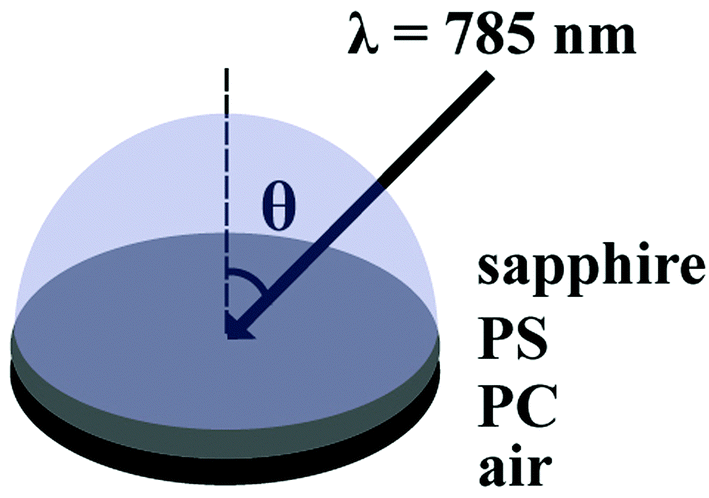 | ||
| Fig. 1 Sample configuration of the bilayer polymer films analysed using SA Raman spectroscopy. The incident angle, θ, of the 785 nm laser was varied from 55.70–65.70° with Raman spectra collected every 0.05°. Raman scattered light from the sample was collected from below the interface using a 10× (0.30 NA) objective. | ||
Sum square electric field (SSEF) calculations
Three dimensional finite-difference-time-domain (FDTD)-based simulations (EM Explorer, San Francisco, CA) were used to calculate the SSEF over each layer of a 4-layer system consisting of a sapphire prism, PS film, PC film, and air. The input values for these calculations included the refractive indices of the layers at 785 nm and the thickness of each layer. The refractive indices of sapphire, PS, and PC for p-polarized 785 nm excitation were 1.762, 1.578, and 1.571, respectively.41–43 In the simulations, the thickness of the prism and air layers were semi-infinite compared to the polymer layers. The total bilayer thickness varied from 1200–3000 nm in 100 nm increments and 3000–3600 nm in 200 nm increments with PS thicknesses varying from 6.25–93.75% (in 6.25% increments) of the total bilayer thickness. The angular range of 55–65° at an angle resolution of 0.05° was selected in order to coincide with the experimental conditions. The SSEF calculations were performed using a Yee cell size of 5 nm and a uniform index of refraction across a layer.Relative Raman scattering cross-section
The calculated SSEF is proportional to the experimental Raman scattering after correcting the SSEF for differences in the PS and PC Raman scattering cross-sections. The relative Raman cross-sections of PS and PC were determined using a PS compact disk case and the PC substrate of a rewritable compact disk. The reflective coating on the compact disk was removed prior to analysis. The thicknesses of the PS and PC samples measured with a digital caliper were 1.01 ± 0.01 mm and 1.09 ± 0.01 mm, respectively. Raman spectra of the PS and PC samples were collected using a 180° backscattering geometry with 785 nm excitation. Excitation and collection of the resulting Raman scattered light was done using a 10× (0.30 NA) objective. The laser power at the sample was 90 mW. The collected Raman spectra represented a two second exposure for a single accumulation. Integrated areas of the PS 1001 cm−1 and PC 889 cm−1 Raman transitions were determined using a Gaussian fit algorithm available in the multipeak fitting package of IGOR Pro (WaveMetrics, Inc., Lake Oswego, OR) [v. 6.3.4.1 (2014)]. The ratio of the integrated area of PS to that of PC was 2.0 ± 0.1. The uncertainty in the relative Raman scattering cross-section was calculated using the standard deviation associated with three replicate determinations of the integrated areas for the selected PS and PC Raman transitions.Data analysis
IGOR Pro 6.4 was used to analyse the SA Raman spectra and results of the SSEF calculations from the FDTD simulations. Peak areas of the 1001 cm−1 and 889 cm−1 PC Raman transitions were determined using a Gaussian fit function with a linear baseline. Plots of Raman intensity versus incident angle were fit to a Lorentzian function in order to identify the angular positions and Raman intensities of the most intense waveguide modes. Matlab (MathWorks, Natick, MA) [v. 8.4.0.150421 (2014)] was used to construct surface plots of the resulting Raman data and FDTD calculations.Results and discussion
SSEF calculations for the PS/PC bilayer films
The goal of this study was to determine the locations of buried interfaces between layers of PS and PC using SA Raman spectroscopy. PS and PC were selected for the present study because they possess similar refractive indices at the 785 nm excitation wavelength and thus optically can be treated as single layer. The first step of this method was to develop models capable of predicting the total bilayer thickness and the composition of the two-polymer samples based on the SSEF, which is related to the SA Raman signal. SSEF values were calculated using FDTD methods. Calculations were performed for bilayer films with total thicknesses ranging from 1200–3600 nm. In order to differentiate between bilayer films within this thickness range, an incident angle range of 55–65° was used. The critical angle required for TIR at the sapphire/PS interface is 63.6°. Extending the angle range to values below 55° permits models of thinner films to be constructed; however, extension of the angle range also increases computing time.FDTD is a numerical analysis technique that is used to perform electromagnetic simulations.44 The FDTD method was originally proposed by Yee in a seminal paper published in 1966.45 The FDTD method employs finite differences as approximations to both the spatial and temporal derivatives that appear in Maxwell's equations. In the present study, 3D FDTD calculations were performed with p-polarized incident light and perfectly matched layers (PMLs) as boundary conditions. The output of the calculations included the percent reflected light from the interface, the integrated electric field over the PS and PC layers, and the electric field profile over the entire 4-layer system at each incident angle. The FDTD method is capable of solving complicated problems; however, it is generally computationally expensive. Depending on the polarization of the incident light, it is possible to use 1D or 2D FDTD calculations to develop a model requiring appreciably less computing time.
Surface plots of the calculated SSEF versus angle and the interface location for bilayer films with total thicknesses of 1300, 2200, and 2700 nm are shown in Fig. 2. (Note: the interface location is represented as either the percent thickness of PS relative to the total bilayer thickness or the ratio of the PS to PC thicknesses, ThickPS/ThickPC, throughout the text.) SSEF values calculated for the PS and PC layers are shown in the left (A, C, and E) and right (B, D, and F) plots, respectively. The most intense waveguide mode was designated mode 0. Additional modes were sequentially assigned (1, 2, etc.) based on their intensities. For example, in the SSEF plots of the 2700 nm thick bilayer film, mode 0 was located at 63.10° for PS (Fig. 2E) and 62.60° for PC (Fig. 2F). Mode 1 for PS and PC were respectively located at 61.75° and 61.25°. As the total bilayer thickness increased, additional modes were observed, and the locations of these modes shifted to higher angles.
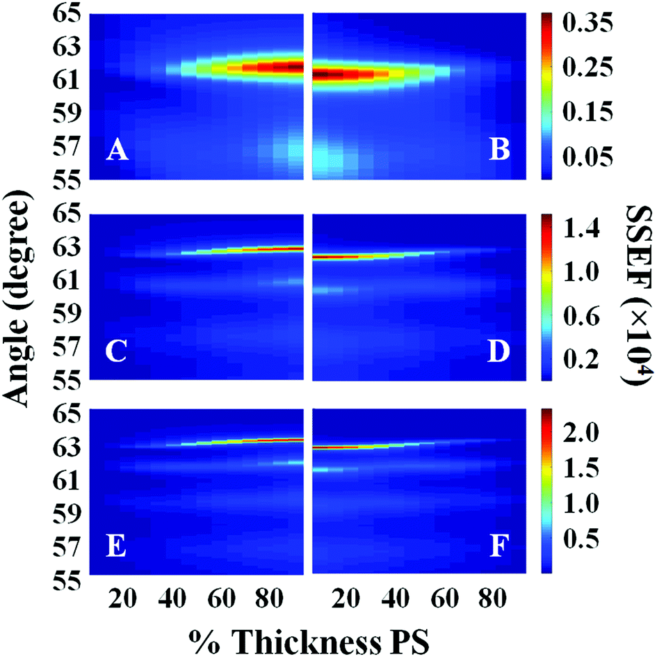 | ||
| Fig. 2 Plots of the calculated SSEF versus interface location (% Thickness PS) and angle for films with total bilayer thicknesses of: (A, B) 1300 nm, (C, D) 2200 nm, and (E, F) 2700 nm. Plots A, C, and E represent the SSEF in the PS layer, and plots B, D, and F represent the SSEF in the PC layer. A schematic of the sample configuration used in the calculations is illustrated in Fig. 1. | ||
The angle difference between modes 0 and 1, hereafter designated as Δθ, is affected by the total bilayer thickness. For example, Δθ calculated for the PS layer (ΔθPS) when it is 25% of the total film thickness was 4.60°, 1.80°, and 1.25° for films with total bilayer thicknesses of 1300, 2200, and 2700 nm, respectively. The SSEF surface plots presented in Fig. 2 also show that there is a minor dependence of Δθ on the location of the buried interface. It is for this reason that the SSEF plots for PS and PC are not mirror images.
The interdependence of Δθ on the total bilayer thickness and interface location can affect the accuracy associated with determinations of total bilayer thickness by SA Raman spectroscopy. Plots of Δθ versus total bilayer thickness are shown in Fig. 3 for PS and PC. Each curve represents a fixed interface location (ThickPS/ThickPC). Using the parameter Δθ and the PS or PC signal, the uncertainty in the bilayer thickness will be greatest for thicker films since the curves approach zero slope. For thinner films, Δθ for PC (ΔθPC) will produce a smaller uncertainty than the PS signal since the latter has a larger distribution of values for a given total bilayer thickness. The PS film is located closer to the prism interface, which makes Δθ more sensitive to the interface location. The uncertainty associated with determinations of total bilayer thickness is further complicated by the limitation of accurately measuring the incident angle. All curves shown in Fig. 3 were fit to power functions; the corresponding fit functions and their root-mean-square residual (RMSR) values are reported in Table 1.
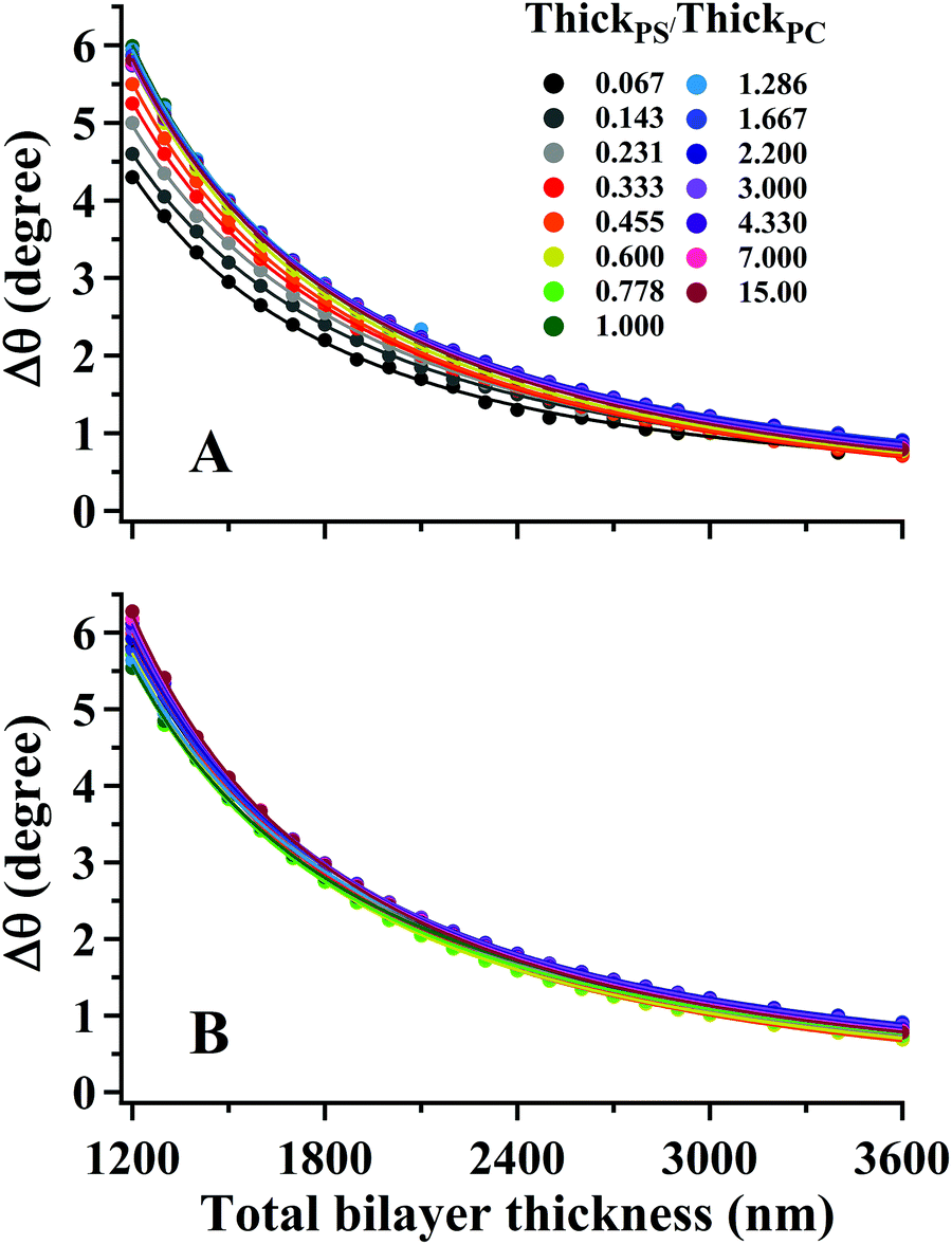 | ||
| Fig. 3 (symbols) Plots of angle difference between modes 0 and 1 (Δθ) in SSEF calculations of bilayer films for (A) PS and (B) PC as a function of the total bilayer thickness. Each curve represents a different buried interface location (ThickPS/ThickPC) from 0.067–15. The solid curves represent a power function fit to the data. The corresponding power fit functions are listed in Table 1. | ||
| Δθ = Δθ0 + A(∑t)B | ||||||||
|---|---|---|---|---|---|---|---|---|
| Angle difference between modes 0 and 1 (Δθ) and total bilayer thickness (∑t) | ||||||||
|
|
Fig. 3A (PS) | Fig. 3B (PC) | ||||||
| Δθ0 | A (×106) | B | RMSRa | Δθ0 | A (×106) | B | RMSRa | |
a Root mean square residual (RMSR) is the mean absolute value of the residuals (r), in which a smaller RMSR indicates a better fit. n is the number of data points.  . .
|
||||||||
| 0.067 | 0.15 | 1.47 | −1.80 | 0.04 | −0.19 | 0.91 | −1.68 | 0.01 |
| 0.143 | −0.07 | 0.34 | −1.58 | 0.02 | −0.19 | 1.07 | −1.70 | 0.01 |
| 0.231 | −0.21 | 0.33 | −1.56 | 0.03 | −0.23 | 1.13 | −1.71 | 0.02 |
| 0.333 | −0.26 | 0.47 | −1.60 | 0.02 | −0.24 | 1.44 | −1.74 | 0.01 |
| 0.455 | −0.18 | 0.89 | −1.69 | 0.02 | −0.22 | 1.59 | −1.76 | 0.02 |
| 0.600 | −0.12 | 1.34 | −1.74 | 0.02 | −0.17 | 1.35 | −1.74 | 0.02 |
| 0.778 | −0.04 | 1.68 | −1.77 | 0.02 | −0.13 | 0.87 | −1.68 | 0.03 |
| 1.000 | 0.07 | 2.50 | −1.83 | 0.01 | −0.07 | 0.78 | −1.67 | 0.03 |
| 1.286 | 0.04 | 1.60 | −1.76 | 0.03 | −0.07 | 0.65 | −1.64 | 0.02 |
| 1.667 | 0.04 | 1.35 | −1.74 | 0.01 | −0.07 | 0.69 | −1.65 | 0.01 |
| 2.200 | −0.06 | 0.81 | −1.67 | 0.01 | −0.07 | 0.85 | −1.67 | 0.01 |
| 3.000 | −0.13 | 0.65 | −1.64 | 0.01 | −0.07 | 1.16 | −1.71 | 0.01 |
| 4.333 | −0.16 | 0.70 | −1.65 | 0.01 | −0.08 | 1.48 | −1.75 | 0.01 |
| 7.000 | −0.18 | 0.74 | −1.65 | 0.01 | −0.09 | 1.85 | −1.78 | 0.02 |
| 15.00 | −0.16 | 0.94 | −1.69 | 0.01 | −0.07 | 2.43 | −1.81 | 0.02 |
In order to account for the interdependence of Δθ on total bilayer thickness and interface location, a second parameter, the SSEF was included in the model. The ratio of the maximum SSEF at mode 0 for PS to the maximum SSEF at mode 0 for PC (SSEFPS/SSEFPC) was multiplied by the relative Raman scattering cross-section in order to correlate SSEFPS/SSEFPC to the experimental Raman scattering intensities of the polymers (IntPS/IntPC). Correction of the SSEF ratio using the relative Raman scattering cross-section was done under the assumption that the photon collection efficiency was consistent across the entire film thickness, which will hold for the low numerical aperture objective used in this study. The Rayleigh length for the optical system is approximately 10 μm.
Curves relating the interface location (ThickPS/ThickPC) to the corrected SSEFPS/SSEFPC ratio and, by extension, the Raman scattering intensities, were constructed for total bilayer thicknesses of 1200–3600 nm. Selected plots of the corrected SSEFPS/SSEFPC ratio versus ThickPS/ThickPC are shown in Fig. 4. All of the curves were fit to power functions over the full ThickPS/ThickPC range of 0.067–15. The resulting fit functions are listed in ESI Table S1.† By defining a range of restricted ThickPS/ThickPC values, the uncertainty in the fit function can be reduced, thereby improving the accuracy of determining the location of the buried interface between the two polymers. The power fit functions corresponding to the ThickPS/ThickPC range of 0.067–3 are listed in Table 2. The average RMSR of the fit functions over the selected range was 0.06.
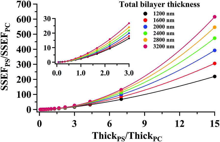 | ||
| Fig. 4 (symbols) Plots of the calculated ratio of SSEFPS/SSEFPC corrected for the relative Raman cross-section as a function of the interface location (ThickPS/ThickPC) for selected total bilayer thicknesses. For clarity, not all generated data have been shown. The solid curves represent a power function fit to the data. The corresponding power fit functions for all curves are listed in Table 2 over the ThickPS/ThickPC range of 0.067–3. | ||
|
|
||||
|---|---|---|---|---|
| When fitting a limited range of
|
||||
| Total thickness (nm) |
|
A | B | RMSRa |
a Root mean square residual (RMSR) is the mean absolute value of the residuals (r), in which a smaller RMSR indicates a better fit. n is the number of data points.  . .
|
||||
| 1200 | 0.09 | 2.22 | 1.82 | 0.03 |
| 1300 | 0.09 | 2.19 | 1.84 | 0.05 |
| 1400 | 0.01 | 2.36 | 1.77 | 0.03 |
| 1500 | 0.04 | 2.28 | 1.85 | 0.02 |
| 1600 | 0.03 | 2.37 | 1.84 | 0.01 |
| 1700 | 0.05 | 2.32 | 1.88 | 0.06 |
| 1800 | 0.01 | 2.44 | 1.86 | 0.03 |
| 1900 | −0.04 | 2.59 | 1.80 | 0.03 |
| 2000 | −0.01 | 2.62 | 1.84 | 0.03 |
| 2100 | −0.01 | 2.64 | 1.85 | 0.05 |
| 2200 | −0.04 | 2.78 | 1.84 | 0.05 |
| 2300 | −0.04 | 2.84 | 1.83 | 0.03 |
| 2400 | −0.08 | 3.03 | 1.80 | 0.04 |
| 2500 | −0.07 | 3.09 | 1.81 | 0.06 |
| 2600 | −0.09 | 3.22 | 1.78 | 0.06 |
| 2700 | −0.09 | 3.27 | 1.80 | 0.07 |
| 2800 | −0.14 | 3.56 | 1.74 | 0.06 |
| 2900 | −0.10 | 3.54 | 1.77 | 0.11 |
| 3000 | −0.13 | 3.75 | 1.75 | 0.07 |
| 3200 | −0.20 | 4.18 | 1.70 | 0.08 |
| 3400 | −0.28 | 4.65 | 1.63 | 0.12 |
| 3600 | −0.23 | 4.92 | 1.65 | 0.25 |

In summary, the unknown sample variables to be determined in this analysis were the total bilayer thickness and ThickPS/ThickPC. These variables, which are defined by the fit functions in Tables 1 and 2, are a function of parameters that can be experimentally determined: (1) Δθ, the angle difference between modes 0 and 1 for PS or PC, and (2) IntPS/IntPC determined at mode 0. Both of the unknown variables can be determined by defining the relevant fit functions for a given sample using Tables 1 and 2 and the two experimentally-determined parameters. The magnitude of the uncertainty for each variable is sample-dependent, as further described below.
SA Raman spectroscopy of bilayer PS/PC films
SA Raman data collected for a 2300 nm thick bilayer film are shown in Fig. 5. The PS and PC film thicknesses were measured by optical profilometry to be 1100 ± 30 and 1200 ± 60 nm, respectively. Raman spectra of the bilayer sample exhibited transitions associated with both PS and PC. The dominant Raman transitions of PS and PC were observed at 1001 and 889 cm−1, respectively. The Raman spectra of PS46–48 and PC49,50 have been previously reported. The 1001 cm−1 shift transition of PS has been assigned to the aromatic ring breathing mode. A transition located at 1028 cm−1 was assigned to a C–H in-plane bending mode of PS.47 The 889 cm−1 shift transition of PC has been previously assigned to both an O–C(O)–O stretch and a C–CH3 stretch. Additional Raman transitions observed at 1108 and 1180 cm−1 were associated with PC. These transitions have been previously assigned to C–O–C stretches43 and in-plane C–H wags.50 In the discussion to follow, all quantitation was performed using the 1001 and 889 cm−1 shift transitions of PS and PC, respectively. In Fig. 5, the maximum intensity for mode 0 of PS, located at 63.52°, possessed an intensity of ∼7000 arbitrary units, and the maximum intensity for mode 0 of PC, located at 63.45°, possessed an intensity of ∼3500 arbitrary units. Considering the approximately equal PS and PC thicknesses for this sample, the ratio of IntPS/IntPC was consistent with that observed for bulk PS and PC samples, which had a relative Raman cross-section ratio of 2.0 ± 0.1.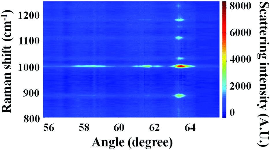 | ||
| Fig. 5 Raman scattering intensity versus angle and Raman shift for a bilayer film consisting of 1100 nm PS and 1200 nm PC layers. Three waveguide modes were observed for both PS and PC within the selected angle region. Modes, 0, 1, and 2 for PS were located at 63.52°, 61.74°, and 58.40°. Modes 0, 1, and 2 for PC were located at 63.45°, 61.79°, and 58.28°. Only the most intense Raman transitions generated appreciable signal at modes 1 and 2. | ||
The application of SA Raman spectroscopy for determinations of total bilayer thickness and buried interface location requires samples with smooth surfaces. The SSEF calculations assume smooth surfaces for the individual layers. Atomic force microscopy (AFM) was used to investigate the surface characteristics of two types of samples: (1) an 1800 nm thick PS film on a glass substrate prior to the deposition of a PC layer and (2) a 2500 nm thick bilayer film consisting of PS and PC thicknesses of 1800 and 700 nm, respectively. The resulting AFM images are shown in ESI Fig. S2.† The root-mean-square roughness of the PS film was 0.29 nm, and the vertical distance between the highest and lowest points of the AFM image was 2.1 ± 0.3 nm. The surface of the PS film (ESI Fig. S2A†) was characterized as a smooth surface because the peak-to-peak roughness was appreciably less than the excitation wavelength. The root-mean-square roughness of the bilayer film (ESI Fig. S2B†) was 0.25 nm, and the vertical distance between the highest and lowest points of the AFM image was 2.6 ± 0.3 nm. Given that the peak-to-peak roughness for the two polymers was similar, and much smaller than the excitation wavelength, the transfer process produced a bilayer sample with a smooth interface between the individual layers.
SA Raman data collected for four PS/PC bilayer films are shown in Fig. 6. The PS and PC thicknesses measured by optical profilometry are listed in Fig. 6 for samples prepared using identical conditions as those used to prepare samples for the SA Raman studies. Optical profilometry is a destructive technique that precluded measuring the individual PS and PC thicknesses on the same samples used for the SA Raman analysis. It was assumed that the PS and PC thicknesses are not altered by the transfer process used to generate the bilayer and that the total bilayer thickness is the sum of the PS and PC thicknesses. In order to test the validity of this assumption, the total bilayer thickness was measured by optical profilometry for each sample after the Raman analysis was complete. The average difference between the sum of the PS and PC thicknesses measured on independent samples and the total bilayer thickness of the SA Raman samples was 6%.
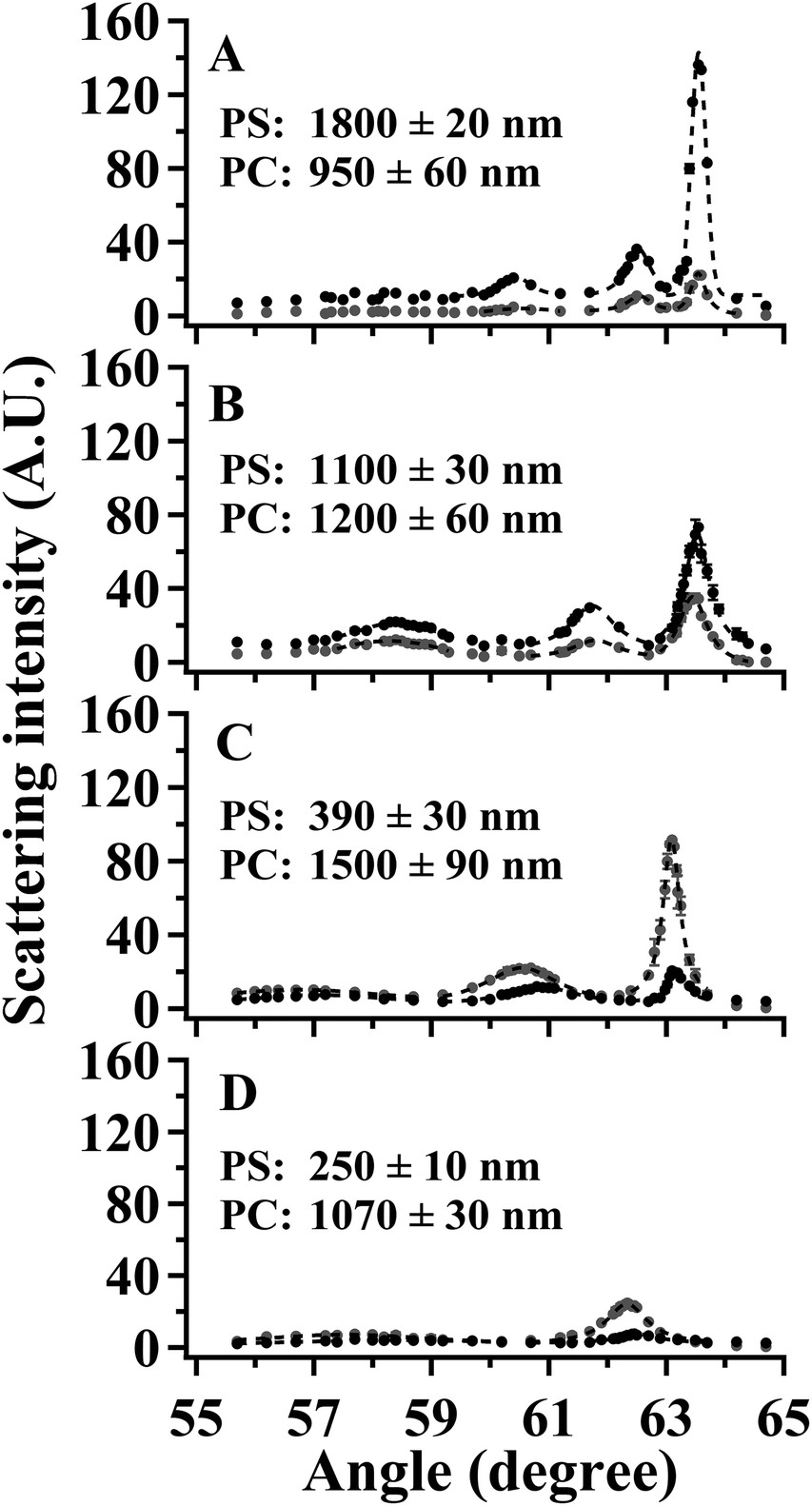 | ||
| Fig. 6 SA Raman intensity for the 1001 cm−1 PS (black) and 889 cm−1 PC (gray) transitions as a function of angle for (A) sample 1, (B) sample 2, (C) sample 3, and (D) sample 4. The dashed lines represent Lorentzian fits for modes 0 and 1. The PS and PC film thicknesses measured by optical profilometry are included in each panel. | ||
The values of Δθ and IntPS/IntPC obtained from the spectra in Fig. 6 are listed in Table 3. The application of SA Raman spectroscopy for determinations of total bilayer and PS thicknesses was performed in two steps. Step 1. The experimentally-determined values of ΔθPS and ΔθPC were input into each of the corresponding fit functions listed in Table 1. Fifteen values representing the curves for ThickPS/ThickPC ranging from 0.067–15 were obtained for each interface. The resulting data are plotted as the gray (PS) and open (PC) symbols in Fig. 7. In order to improve the clarity of the constructed plots, the ThickPS/ThickPC ratios have been restricted to a range of 0 to 5. Step 2. The ratio of IntPS/IntPC determined at mode 0 for each sample was input into the fit functions listed in Table 2 to obtain twenty-two values plotted as black symbols in Fig. 7. The x- and y-values at the intersections of the fit functions (ESI Tables S2 and S3†) represent the location of the buried interface and the total bilayer thickness, respectively.
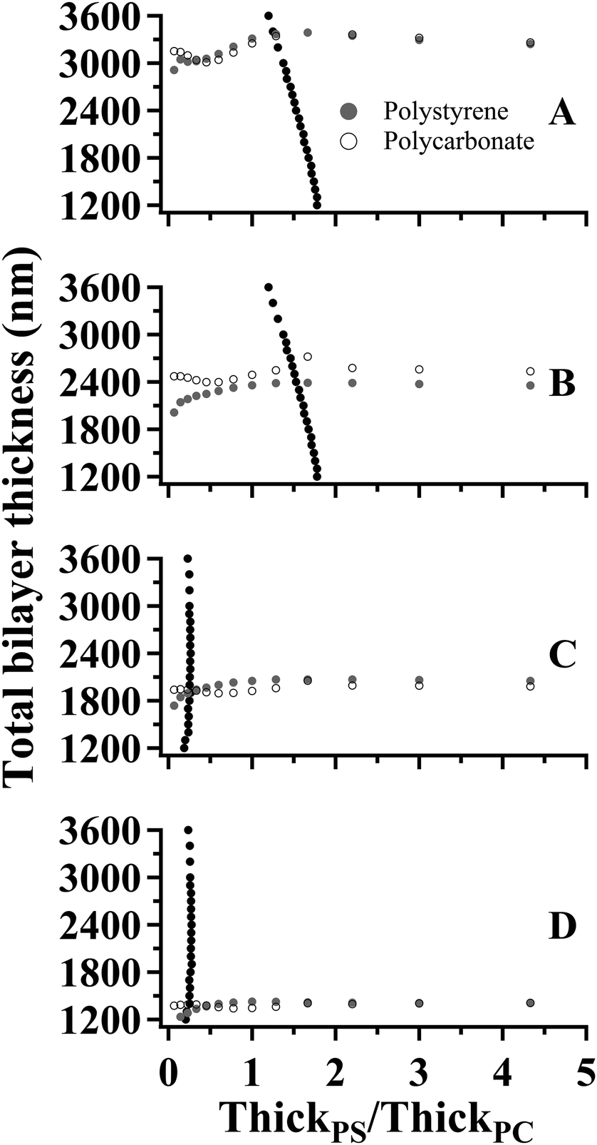 | ||
| Fig. 7 Plots of total bilayer thickness versus interface location (ThickPS/ThickPC) constructed using the fit functions listed in Tables 1 and 2 and the SA Raman spectroscopy data (Table 3) collected for: (A) sample 1, (B) sample 2, (C) sample 3, and (D) sample 4. | ||
| Δθ (°) |
|
Total bilayer thickness (nm) | PS thickness (nm) | ||||
|---|---|---|---|---|---|---|---|
| PS | PC | SA Raman spectroscopya | % Differenceb | SA Raman spectroscopya | % Differenceb | ||
| a Average of PS and PC determinations; uncertainties represent standard deviation. b Compared to optical profilometry values. | |||||||
| Sample 1 | 1.0 ± 0.1 | 1.0 ± 0.1 | 6.4 ± 0.7 | 3350 ± 10 | 19.7 | 1880 ± 10 | 4.3 |
| Sample 2 | 1.8 ± 0.1 | 1.6 ± 0.1 | 1.8 ± 0.1 | 2380 ± 70 | 3.4 | 1040 ± 30 | 5.6 |
| Sample 3 | 2.3 ± 0.1 | 2.5 ± 0.1 | 0.20 ± 0.01 | 1920 ± 20 | 1.6 | 390 ± 10 | 0.1 |
| Sample 4 | 4.4 ± 0.3 | 4.6 ± 0.3 | 0.22 ± 0.01 | 1330 ± 80 | 0.8 | 250 ± 30 | 0.1 |
Considering the range of ThickPS/ThickPC represented in Fig. 7, there are appreciable differences in the total bilayer thicknesses calculated using ΔθPS and ΔθPC for values below 0.5. Determinations of total bilayer thickness within this region will inherently possess greater uncertainties than those performed at larger thickness ratios. As the value of ThickPS/ThickPC increased, the total bilayer thicknesses calculated using ΔθPS and ΔθPC converged for the data shown in Fig. 7A, C and D, indicating good agreement between the two values. The curves presented in Fig. 7B possessed an appreciable difference in the total bilayer thicknesses calculated using the values of ΔθPS and ΔθPC across the entire range of ThickPS/ThickPC. This data set had a smaller value of ΔθPC compared to the expected calculated value by 2°. When the smaller value of ΔθPC is input into the fit functions (Table 1) the total bilayer thickness is overestimated.
The total bilayer and PS thicknesses determined by SA Raman spectroscopy are summarized in Table 3. The listed values represent averages of the total bilayer thickness and interface locations determined using the PS and PC fit functions. Percent differences between the total bilayer thicknesses determined by SA Raman spectroscopy and optical profilometry were 0.8% (sample 4) and 1.6% (sample 3) and increased for the thicker samples, as expected based on the preceding discussion of Fig. 3. The accuracy associated with thickness determinations for samples thicker than ∼2300 nm can potentially be improved through the construction of calibration models based on the angle difference between modes 1 and 2, or even higher modes. The angle difference for higher order modes will be larger for thicker films than the angle difference between modes 0 and 1, as shown in Fig. 2.
The percent difference between the SA Raman spectroscopy and optical profilometry determinations of the buried interface location (PS thickness) was less than 6% for all four samples. The small percent differences indicate that accurate determinations of the buried interface location between two optically homogeneous polymers can be obtained using the outlined method. When considering the capabilities of three complementary Raman techniques: TIR, SA, and confocal Raman spectroscopy, the methodology presented herein fills a missing gap for measuring films of a few hundred nanometers to a few micrometers thickness with tens-of-nanometer precision. The lower limit is governed by the polymer thickness required to form a waveguide, while the upper thickness is governed by the optics. To increase the polymer thickness range that can be studied with the SA Raman methodology, a shorter excitation wavelength could be employed to extend the range at lower thicknesses. In addition, the incident angle range could also be extended, as already discussed.
Conclusions
Near-infrared SA Raman spectroscopy has been shown to be a viable, non-destructive method for determinations of chemical composition, total bilayer thickness, and buried interface location. The latter two parameters determined using this method were in agreement with independent measurements performed using optical profilometry. For the analysis of thin film compositions, SA Raman spectroscopy offers the advantage of at least an order of magnitude improvement in axial spatial resolution compared to wide-field and confocal Raman spectroscopy. While the two polymers used in this study had similar indices of refraction, the method is expected to be applicable to the analysis of polymer bilayers where the refractive indices of the layers vary. The limits of suitable indices of refraction, however, need to be studied. SA Raman spectroscopy is applicable to the analysis of multi-layered polymer films when information regarding chemical composition and thickness is required.Abbreviations
| AFM | Atomic force microscopy |
| ATR-FT-IR | Attenuated total (internal) reflection-Fourier transform infrared |
| FDTD | Finite-difference-time-domain |
| SSEF | Sum square electric field |
| PC | Polycarbonate |
| PS | Polystyrene |
| RMSR | Root-mean-square residual |
| SA | Scanning angle |
| TIR | Total internal reflection |
Acknowledgements
This research is supported by the U.S. Department of Energy, Office of Basic Energy Sciences, Division of Chemical Sciences, Geosciences, and Biosciences through Ames Laboratory. The Ames Laboratory is operated for the U.S. Department of Energy by Iowa State University under Contract No. DE-AC02-07CH11358. The authors thank Wyman Martinek for his assistance with the optical profilometry measurements.Notes and references
- Y. Wang, A. Hongo, Y. Kato, T. Shimomura, D. Miura and M. Miyagi, Appl. Opt., 1997, 36, 2886–2892 CrossRef CAS.
- L. Eldada and L. W. Shacklette, IEEE J. Sel. Top. Quantum Electron., 2000, 6, 54–68 CrossRef CAS.
- X. Li, X. H. Yu and Y. C. Han, J. Mater. Chem. C, 2013, 1, 2266–2285 RSC.
- S. W. Kim and G. H. Kim, Appl. Opt., 1999, 38, 5968–5973 CrossRef CAS.
- M. Conroy, Wear, 2009, 266, 502–506 CrossRef CAS PubMed.
- D. Mansfield , Proc. SPIE 7101, Advances in Optical Thin Films III, 710101 (October 15, 2008).
- F. Madani-Grasset, N. T. Pham, E. Glynos and V. Koutsos, Mater. Sci. Eng., B, 2008, 152, 125–131 CrossRef CAS PubMed.
- P. M. Fredericks, in Handbook of Vibrational Spectroscopy, ed. J. M. Chalmers and P. R. Griffiths, John Wiley & Sons, Ltd., Chichester, 2002, vol. 2, pp. 1493–1507 Search PubMed.
- P. M. Fredericks, in Vibrational Spectroscopy of Polymers: Principles and Practice, ed. N. J. Everall, J. M. Chalmers and P. R. Griffiths, John Wiley & Sons, Inc., Hoboken, 2007, pp. 179–200 Search PubMed.
- N. J. Harrick, Phys. Rev. Lett., 1960, 4, 224–226 CrossRef CAS.
- N. J. Harrick, J. Phys. Chem., 1960, 64, 1110–1114 CrossRef CAS.
- N. J. Harrick, Ann. N. Y. Acad. Sci., 1963, 101, 928–959 CrossRef CAS PubMed.
- N. J. Harrick, in Internal Reflection Spectroscopy, Interscience, New York, 1967 Search PubMed.
- A. J. Sommer, in Modern Techniques in Applied Molecular Spectroscopy, ed. F. M. Mirabella, Wiley-Interscience, New York, 1998, pp. 291–322 Search PubMed.
- N. J. Everall, Appl. Spectrosc., 2000, 54, 773–782 CrossRef CAS.
- N. J. Everall, Appl. Spectrosc., 2000, 54, 1515–1520 CrossRef CAS.
- N. Everall, J. Lapham, F. Adar, A. Whitley, E. Lee and S. Mamedov, Appl. Spectrosc., 2007, 61, 251–259 CrossRef CAS PubMed.
- N. J. Everall, Appl. Spectrosc., 2009, 63, 245A–262A CrossRef CAS PubMed.
- T. Ikeshoji, Y. Ono and T. Mizuno, Appl. Opt., 1973, 12, 2236–2237 CrossRef CAS PubMed.
- T. Takenaka and T. Nakanaga, J. Phys. Chem., 1976, 80, 475–480 CrossRef CAS.
- D. A. Woods and C. D. Bain, Analyst, 2012, 137, 35–48 RSC.
- R. Iwamoto, M. Miya, K. Ohta and S. Mima, J. Chem. Phys., 1981, 74, 4780–4790 CrossRef CAS PubMed.
- L. G. Tisinger and A. J. Sommer, Microscopy and Microanalysis, 2004, 10, 1318–1319 CrossRef.
- A. O. Kivioja, A. S. Jaaskelainen, V. Ahtee and T. Vuorinen, Vib. Spectrosc., 2012, 61, 1–9 CrossRef CAS PubMed.
- N. H. Fontaine and T. E. Furtak, Phys. Rev. B: Condens. Matter, 1998, 57, 3807–3810 CrossRef CAS.
- Y. Levy, C. Imbert, J. Cipriani, S. Racine and R. Dupeyrat, Opt. Commun., 1974, 11, 66–69 CrossRef CAS.
- J. F. Rabolt, R. Santo and J. D. Swalen, Appl. Spectrosc., 1979, 33, 549–551 CrossRef CAS.
- J. F. Rabolt, R. Santo and J. D. Swalen, Appl. Spectrosc., 1980, 34, 517–521 CrossRef CAS.
- J. F. Rabolt, N. E. Schlotter and J. D. Swalen, J. Phys. Chem., 1981, 85, 4141–4144 CrossRef CAS.
- C. G. Zimba, V. M. Hallmark, S. Turrell, J. D. Swalen and J. F. Rabolt, J. Phys. Chem., 1990, 94, 939–943 CrossRef CAS.
- D. R. Miller, O. H. Han and P. W. Bohn, Appl. Spectrosc., 1987, 41, 245–248 CrossRef CAS.
- D. R. Miller, O. H. Han and P. W. Bohn, Appl. Spectrosc., 1987, 41, 249–255 CrossRef CAS.
- P. W. Bohn, TrAC, Trends Anal. Chem., 1987, 6, 223–233 CrossRef CAS.
- D. R. Miller and P. W. Bohn, Anal. Chem., 1988, 60, 407–411 CrossRef CAS.
- D. R. Miller and P. W. Bohn, Appl. Opt., 1988, 27, 2561–2566 CrossRef CAS PubMed.
- N. H. Fontaine and T. E. Furtak, J. Opt. Soc. Am. B, 1997, 14, 3342–3348 CrossRef CAS.
- F. Ishizaki and M. Kim, Jpn. J. Appl. Phys., 2008, 47, 1621–1627 CrossRef CAS.
- K. J. McKee and E. A. Smith, Rev. Sci. Instrum., 2010, 81, 043106 CrossRef PubMed.
- M. W. Meyer, V. H. T. Nguyen and E. A. Smith, Vib. Spectrosc., 2013, 65, 94–100 CrossRef CAS PubMed.
- G. F. Schneider, V. E. Calado, H. Zandbergen, L. M. K. Vandersypen and C. Dekker, Nano Lett., 2010, 10, 1912–1916 CrossRef CAS PubMed.
- I. H. Malitson, J. Opt. Soc. Am., 1962, 52, 1377–1379 CrossRef CAS.
- F. Ay, A. Kocabas, C. Kocabas, A. Aydinli and S. Agan, J. Appl. Phys., 2004, 96, 7147–7153 CrossRef CAS PubMed.
- S. N. Kasarova, N. G. Sultanova, C. D. Ivanov and I. D. Nikolov, Opt. Mater., 2007, 29, 1481–1490 CrossRef CAS PubMed.
- D. M. Sullivan, in Electromagnetic Simulation Using the FDTD Method, IEEE Press, Piscataway, 2000 Search PubMed.
- K. S. Yee, IEEE Trans. Antennas Propag., 1966, 14, 302–307 CrossRef.
- A. Palm, J. Phys. Chem., 1951, 55, 1320–1324 CrossRef CAS.
- W. M. Sears, J. L. Hunt and J. R. Stevens, J. Chem. Phys., 1981, 75, 1589–1598 CrossRef CAS PubMed.
- C. H. Jones and I. J. Wesley, Spectrochim. Acta, Part A, 1991, 47, 1293–1298 CrossRef.
- B. H. Stuart and P. S. Thomas, Spectrochim. Acta, Part A, 1995, 51, 2133–2137 CrossRef.
- S. N. Lee, V. Stolarski, A. Letton and J. Laane, J. Mol. Struct., 2000, 521, 19–23 CrossRef CAS.
Footnotes |
| † Electronic supplementary information (ESI) available: Calibration curves of PS and PC thicknesses versus concentration measured by optical profilometry and AFM images of (1) a PS film on a glass substrate and (2) a bilayer PS/PC film on a glass substrate can be found in supplemental information Fig. S1 and S2, respectively. In addition, tables listing the fit functions for the curves shown in Fig. 4 and the fit functions for the curves shown in Fig. 7 can be found in supplemental information Tables S1–S3, respectively. See DOI: 10.1039/c4an02240h |
| ‡ These authors contributed equally to the work. |
| This journal is © The Royal Society of Chemistry 2015 |