
 Open Access Article
 This Open Access Article is licensed under a Creative Commons Attribution-Non Commercial 3.0 Unported Licence
Self-cleaning properties in engineered sensors for dopamine electroanalytical detection†
Guido
Soliveri‡
ab,
Valentina
Pifferi‡
ab,
Guido
Panzarasa
c,
Silvia
Ardizzone
ab,
Giuseppe
Cappelletti
ab,
Daniela
Meroni
ab,
Katia
Sparnacci
c and
Luigi
Falciola
*ab
aDipartimento di Chimica, Università degli Studi di Milano, Via Golgi 19, 20133 Milano, Italy. E-mail: luigi.falciola@unimi.it
bConsorzio Interuniversitario Nazionale per la Scienza e Tecnologia dei Materiali (INSTM), Via Giusti 9, 50121 Firenze, Italy
cDipartimento di Scienze e Innovazione Tecnologica, Università del Piemonte Orientale “Amedeo Avogadro”, Viale T. Michel 11, 15100 Alessandria, Italy
First published on 12th January 2015
Abstract
Fouling and passivation are the major drawbacks for a wide applicability of electroanalytical sensors based on nanomaterials, especially in biomedical and environmental fields. The production of highly engineered devices, designed ad hoc for specific applications, is the key factor in the direction of overcoming the problem and accessing effective sensors. Here, the fine-tuning of the system, composed of a highly ordered distribution of silver nanoparticles between a bottom silica and a top titania layer, confers multifunctional properties to the device for a biomedical complex challenge: dopamine detection. The crucial importance of each component towards a robust and efficient electroanalytical system is studied. The total recovery of the electrode performance after a simple UV-A cleaning step (self-cleaning), due to the photoactive interface and the aging resistance, is deeply investigated.
Introduction
New types of sensing devices have been recently attracting tremendous attention because of environmental concerns and biomedical demands.1–7 The fast development of nanotechnology has paved the way for the design of tailored systems exhibiting superior properties.8–12Composite oxide/metal systems employing silver nanoparticles (Ag NPs) have gained increasing attention8,9,13 especially in the case of electroanalysis for trace detection, due to Ag NPs’ unique properties.8,9 Silver possesses the highest electrical conductivity and good stability at different potentials and pH, and, more relevantly, it shows good electrocatalytic properties compared to other metals. For these reasons, it is a widely used electrode material and the advent of nanotechnology has further improved its possibilities. As a matter of fact, compared to the traditional bare noble metal electrodes, nanostructured surface morphologies can enhance the response of the sensing system. The high surface to volume ratio and appropriate nano-dimensions enormously increase the availability of interaction sites for the analyte, improving the sensitivity and lowering detection limits, which are the fundamental characteristics for trace analysis. Moreover, the small dimensions may allow controlling the sensing process locally, in terms of analyte diffusion mechanism and site-analyte recognition. The effects described above are particularly maximized in the case of well-ordered structures.
A problem often encountered during the use of these nanosized, complex devices, is represented by the passivation and fouling phenomena leading to a poor reusability.1,8
Passivation and fouling are mainly due to the electrochemically produced byproducts or interfering compounds present in the analyzed complex real matrix, chemisorbed on the electrode surface. The conventional cleaning procedures applied to bulk metal electrodes (mechanical or electrochemical etching) are inapplicable in the case of metal nanoparticles, since these systems can be irreversibly modified or the nanoparticles even removed from the electrode surface. This is a critical limitation for a commercial sensor, which, apart from high sensitivity, low detection limits and high selectivity, should be also characterized by portability, online and onsite usability and especially re-usability.1,4 In this context, self-cleaning electrodes could represent a step beyond the current state of the art procedures.
Self-cleaning materials mediated by UV and visible light have played the main role in both fundamental and applicative studies in the last 30 years.14,15 Self-cleaning coatings,16 windows and cements, and also self-sterilizing medical devices and surgical rooms are, nowadays, appealing products in the market.14 Titanium dioxide (TiO2) is the main protagonist for the present products and products under development. TiO2 was first investigated thoroughly for its highly attractive photo-oxidative and photo-reductive powers, and for its appealing band-gap (3.2 eV for anatase and 3.0 eV for rutile). Besides its semiconductor properties, the oxide shows high bio-compatibility, high refractive index and, above all, high availability and low costs.
A very recent work by Kamat et al.17 has reported a “detect and destroy” approach for SERS analyses, in which the combination of SERS experiments supported by Ag NPs, with the photocatalytical degradation of a molecule by TiO2 is described.
On the other hand, to the authors’ best knowledge, the study of self-cleaning layers potentially applicable on any electrode surface to prevent passivation, caused either by silver oxidation or by the presence of interferents, has not been explored yet. Literature reports only a few examples of self-cleaning electrodes for hydrogen detection,18 and for methanol electro-oxidation or glucose determination.19,20 These systems are based on anodized titania nanotube supports decorated with noble metals (Pt and Pd), where the titania photoeffect is exploited to restore the activity of the device. In the literature, neither a suitable electrode design for re-usability, nor a deep study of fouling/cleaning effects on the electroanalytical parameters is investigated.
In this very promising context, we propose an innovative self-cleaning engineered device to be used as an electroanalytical sensor. The device is composed of a transparent metal-oxide composite multilayer in which Ag NPs are deposited to give a controlled and organized structure between a bottom silica and a top titania layer. Each component of the device was chosen for its relevant properties: the silica layer was essential to govern the distribution of silver nanoparticles, which were the actual sensing tools, imparting electrocatalytic properties and conductivity between the two semiconducting oxides; the top titania film was not only used to confer the self-cleaning properties, but also to protect Ag NPs from oxidation and deterioration.
In order to check the applicability of the designed device in a real, challenging and complex system, the electroanalytical detection of dopamine was studied.21,22 Dopamine is a neurotransmitter with great biomedical and analytical properties, since the molecule's anomalous levels are diagnostic for Parkinson's disease and for many neurological pathologies. In the literature, its determination has been carried out by different electrodes and strategies,23–25 but, in almost all cases, fouling and passivation of the electrode surface affected the measurements. In particular, the chemisorption of dopamine or of its byproducts at metal and oxide interfaces makes the reusability of the electrode generally impossible.21 The present self-cleaning sensor is ad hoc designed for the detection of such critical molecules, affording a total sensitivity recovery after fouling and cleaning by a simple UV irradiation step. Moreover, aging, over-usage and environmental conditions did not introduce appreciable modifications in the initial characteristics of the electrode.
Results and discussion
Device assembly and structure
The device, described in the present work, was engineered with the aim of tuning its photocatalytic and electrochemical properties in order to obtain an electroanalytical sensor for the detection of molecules with biomedical interest. We controlled the synthesis in order to promote the self-cleaning properties and tune the electrocatalytic features by modulating the sandwich composition and Ag NP organization, preserving the film transparency. Fig. 1a shows the material architecture. | ||
| Fig. 1 Device structure: (a) schematic description of the architecture, (b) X-ray diffraction pattern of the titania top layer and (c) SEM cross section of the film. | ||
Each layer/component was finely designed in order to control the final performance: support, silica layer, bifunctional siloxane ((3-aminopropyl)triethoxysilane, APTES), Ag NPs, titania. As the support, a conductive glass, withstanding calcination, FTO, was selected. The subsequent presence of a silica layer was chosen in order to promote the dispersion of AgNPs. The layer of silica was obtained by dip coating the FTO surface in a non-aqueous sol, synthesized according to the procedure reported by Wang et al.26 The subsequent calcination conditions were chosen in order to decompose the organic components of the sol while maintaining the film transparency and increasing its mechanical stability and adhesion onto the support. The roles played by time, temperature and atmosphere were preliminarily studied to tune the reactivity of the surface. A calcination step of one hour at 400 °C under N2 flow was finally adopted. The calcined silica layer was further grafted by a bifunctional siloxane in order to promote the stable attachment of Ag NPs. APTES was chosen as a coulombic binder between the SiO2 surface and the Ag NPs. APTES ethoxy groups generally react with –OH groups on the oxide surface, exposing –NH3+ groups at the interface.27 The negatively charged Ag NPs (Z-potential measurement, ESI, Fig. S1†) strongly interact with –NH3+ groups, so that the number and the arrangement of APTES molecules highly influence the concentration and disposition of Ag NPs at the surface.
The Ag NPs, synthesized by the procedure of Panzarasa,28 were stabilized by PVP10 to avoid the presence of agglomerates and multilayers on the functionalized surface. The HRTEM image (Fig. 2a) shows particles of around 11 nm diameter (10.8 ± 1.3 nm) with high crystallinity (the lattice spacing of ∼230 pm corresponds to the (111) planes of a silver fcc cell) and quite sharp distribution. The aqueous particle suspension presented the typical plasmonic resonance associated with Ag NPs of dimensions lower than 30 nm (Fig. 2b inset).29 After being dipped for 15 minutes in such a suspension, the material showed the orange colour correlated with the spectrum as shown in Fig. 2b. The red-shift of the band is derived from a change of environment, as reported by Evanoff et al.30
 | ||
| Fig. 2 (a) HRTEM image of Ag NPs, showing high crystallinity and a lattice spacing of about 230 pm; (b) UV-Vis spectrum of Ag NPs grafted on the silica surface; inset: UV-Vis spectrum of the Ag NP suspension. | ||
Finally, the engineered sensor is covered by a TiO2 layer with the aim to impart photoactivity and self-cleaning properties. The oxide external layer was demonstrated to confer further crucial properties to the material, such as protection for the Ag NPs from unavoidable oxidation/deactivation ensuing from the contact with the environment. The TiO2 film was obtained by dip-coating the multilayer device in a non-aqueous sol, synthesized following a procedure previously developed by our group.31 Temperature and, particularly, the atmosphere of calcination were chosen in order to prevent Ag oxidation. In the absence of a protective TiO2 layer, Ag degradation is generally observed after few days of exposure to environmental conditions, dramatically changing both the chemical nature and the morphology of such particles. We tested different times and conditions for TiO2 crystallization and growth. A fast calcination for 1 hour at 400 °C under N2 flow allowed the organic compounds mineralization and the growth of oxide crystallinity, without altering the film transparency (ESI, Fig. S2†).
The XRD lines (Fig. 1b) of the sandwich show the predominance of the anatase polymorph, with traces of brookite. The peaks of cassiterite (SnO2), which are related to the FTO support are also appreciable. The size of anatase crystallites was evaluated to be 17 nm. The SEM cross-section image, shown in Fig. 1c, reveals two distinct and homogeneous layers, 550 nm and 150 nm in thickness, for SiO2 and TiO2, respectively. Thickness data were confirmed by FILMETRICS® analysis, comparing the experimental reflectance spectrum with a calculated one (ESI, Fig. S3†), showing reproducible values in different areas of the film. The SEM top image (ESI, Fig. S4†) shows a good homogeneity of the surface.
The role of silver in electrocatalysis both as a massive electrode and as a nanoparticle has been amply discussed in the literature32–34 also for sensing applications,8,9,35 where Ag can favourably change the potential of redox reactions, also allowing interference management.
The actual presence of Ag in the device was shown by cyclic voltammetry performed in the absence of an electroactive probe. Electrodes without Ag behaved similar to bare FTO, showing completely capacitive voltammograms without peak formation (Fig. 3a, curve 1), typical of oxide materials. In the presence of Ag (Fig. 3a, curve 2 and 3), oxidation and reduction peaks around +0.25 V (SCE) and +0.1 V (SCE) appeared, as generally reported.36,37
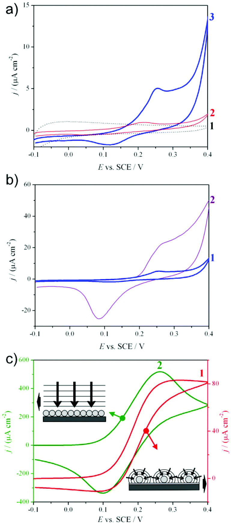 | ||
| Fig. 3 Cyclic voltammograms in the (a, b) absence or (c) presence of the K4[Fe(CN6)] probe molecule. Study of (a) the effect of titania layer (curve 1: FTO + SiO2 + TiO2; curve 2: FTO + SiO2 + Ag; curve 3: FTO + SiO2 + Ag + TiO2), (b) the effect of a silica layer (curve 1: FTO + SiO2 + Ag + TiO2, curve 2: FTO + Ag + TiO2), (c) the distribution of Ag NPs (curve 1: FTO + SiO2 + Ag; curve 2: FTO + Ag). | ||
Moreover, silver, due to its reactive nature, can be oxidized by oxygen present in the air, with passivation effects. To avoid this phenomenon, protective oxides are often used on metal surfaces.38 In our case, the titania layer provided a protective action for Ag NPs. This effect can be proved by comparing the final electrode (Fig. 3a, curve 3) with a device prepared in the same manner, but without the final TiO2 layer (Fig. 3a, curve 2). In the case of titania covered silver nanoparticles, higher Ag peak currents were observed, reflecting the presence of more active and non-oxidized silver nanoparticles.
A key point to take into consideration in the use of modified electrodes supporting silver for sensor applications is the density, distribution and organization of nanoparticles on the electrode surface.8 In electroanalysis, the analyte reacts on the surface of the electrode, generating an increase of the measured current. The resulting signal is the sum of the capacitive background current and of the reaction current, which is solely related to the analyte concentration. The voltammogram shape is related to the NP size and density:39,40 a steady-state sigmoidal step can be registered for a convergent independent diffusion at low NP coverage (Fig. 3c, schematic 1), while a peak is obtained in the case of a planar diffusion regime at high NP coverage (Fig. 3c, schematic 2).
In order to obtain high sensitivity and low detection limits, high faradaic and low capacitive currents are preferred. An optimal disposition for this purpose is an ordered array of well isolated nanoparticles, where the convergent mass transport must be predominant.40–42 In this case, the current response is greater with respect to that of a macroelectrode. In fact, while the current at a macroelectrode follows the Randles–Sevčik equation (eqn (1)):43
| Ipeak = 2.69 × 10⁵n3/2D1/2Cbulkv1/2A | (1) |
| Ilim = 8.71nFDCbulkr | (2) |
| Itot = Ilim[A/(10r)2] = (8.71nFDCbulkA)/(100r) | (3) |
From eqn (3), it is evident that the current depends on the particle radius (the smaller, the better) and is independent of the potential scan rate, since a convergent mechanism is attained.
Using typical values for the parameters and a value of r = 10 nm, a current increase of seven hundred times can be obtained8 with respect to the macroelectrode.
It is worthwhile to note that the above considerations are valid assuming that the nanoparticles are sufficiently far apart so as to be diffusionally independent. Too closely packed electrodes result in the overlapping of the diffusion layers, characterized by the loss of convergent diffusion. The nearest-neighbour NP's minimum distance of 10r required for diffusional independency, although debated,40,45 is assumed to be a good indicative value.8
Moreover, the NP array is characterized by a larger surface area-to-volume ratio of the electrocatalytic material. This fact lowers the costs of the electrodes and, on increasing the active sites, enhances the signal-to-noise ratio, particularly abating the capacitive background currents, which are dependent on the real active surface area.8
Devices based on ordered arrays are normally produced lithographically by long, difficult and costly procedures and only a few papers rely on simple and effective techniques,41 since simpler methodologies usually produce random or uncontrollable distributions. The preparation method presented in this work allows for the obtainment of organized and regularly distributed arrays of Ag NPs by a simple and low cost procedure. The key factor is represented by the interaction sites for silver, produced by –NH3+ APTES groups, in terms of quantity and distribution. We carefully tuned the conditions of APTES deposition and silica calcination in order to produce well-organized and separated sites. Following the method reported by Moon et al.,46 we collected evidence that the concentration of amino groups at the surface was almost double for bare FTO (10 (NH2 nm−2)) compared to FTO covered by silica (5 (NH2 nm−2)) under the same conditions. In the latter case, a lower quantity of silver nanoparticles was expected on the silica layer. Fig. 3b shows voltammograms registered for the two Ag NP electrodes, differing only with respect to the presence or absence of the silica layer. When Ag nanoparticles are deposited on silica (Fig. 3b, curve 1), a lower quantity of the metal is present, as demonstrated by the above considerations, and a lower peak current is registered in comparison with Ag NPs directly deposited on bare FTO (Fig. 3b, curve 2). It is important to highlight that the current registered in the presence of the non-conductive silica layer is, anyway, really high and of the same order of magnitude as the electrode without silica. The contribution brought by the distribution (array) of isolated NPs (convergent diffusion) is evident and will be of paramount importance in the detection of analyte at trace levels, as already explained.
The distribution of silver nanoparticles on silica was studied by registering cyclic voltammograms, this time in the presence of a redox probe (K4[Fe(CN)6]), before TiO2 deposition (Fig. 3c). Only in the presence of a redox reaction the diffusion mechanism and, as a consequence, the distribution of nanoparticles can be studied. Fig. 3c curve 1 shows a step-shaped voltammogram typical of a convergent diffusion mechanism on isolated ordered nanoparticles (schematic 1) in the case of Ag NPs anchored on silica. On the other hand, a peak-shaped voltammogram (Fig. 3c, curve 2), reflecting a semi-infinite diffusion on non-isolated particles (schematic 2), was observed in the case of silver directly deposited on FTO.
Fig. 4 shows electrochemical impedance spectroscopy (EIS) measurements in the presence of the redox probe K4[Fe(CN)6]. The analyses were performed on different electrodes at different steps of preparation and at different compositions of the sandwich. Impedance analysis measures the current response of the device to an external potential variation and allows modelling the systems by an electrical circuit. In the complex plane plots (Fig. 4, Bode plots shown in ESI, Fig. S5†), the semicircle shape common to all the combinations can be represented by the same equivalent circuit (Fig. 4, inset), composed of the solution resistance (RΩ) in series with a parallel formed by the charge transfer resistance (RCT) and double layer capacitance (CPEDL). This trend of experimental data and circuits derived from modelling is typical for a redox reaction of a model probe at the electrode. From the diameter of the semicircle, we obtained the values of the charge transfer resistance (Fig. 4, table), critical to describe the electron transfer between the model probe and the electrode. As expected, these values increase, enhancing the number of layers, while the introduction of Ag NPs produces a drastic decrease in resistance in otherwise identical conditions. We demonstrated the crucial presence of Ag nanoparticles in order to enhance the electrode conductivity in the architecture of our final device, since electrons of the probe reaction can more easily pass through the two semiconductor layers.
 | ||
| Fig. 4 Complex plane plot spectra for all the electrode architectures, registered at + 0.1 V (SCE) in the presence of the model probe molecule K4[Fe(CN6)]; inset: equivalent circuit used to fit data. Table: charge transfer resistance (RCT) values calculated from the fitting. | ||
Top layer photoactivity
The role played by TiO2 as an external layer in protecting Ag NPs from oxidation has already been discussed.The self-cleaning properties of the final device can be achieved by the presence of TiO2 on the top of the sandwich. The accurate engineering of the final layer aimed at imparting photoactivity at the interface without altering transparency, mechanical properties and the state of Ag NPs. As a matter of fact, crystallinity growth (and the degradation of the organic components) promoted by the calcination step is crucial in order to impart photoactivity.14 Here, the careful modulation of the sol composition associated with a rapid calcination at 400 °C under an inert atmosphere not only assured high photoactivity under UV-A irradiation, but also preserved the transparency of the film. Photoactivity was proved by the degradation of chemisorbed hydrophobic organic chains (SILRES 1701) monitoring the water contact angle decrease by a procedure previously reported in literature for the simulation of finger print/oily stain self-cleaning.47,48 The presence of silane molecules chemisorbed at the electrode surface (Fig. 5, schematic), shifted the θw value from hydrophilic (30–0°) to ∼110°. Under irradiation in the UV region, electron–hole pairs were created at the TiO2 interface. This makes the surface reactive. Peroxide and superoxide radicals were generated,14 reacting and oxidizing the organic chains of the chemisorbed siloxane, bringing back θw to the hydrophilic value.
 | ||
| Fig. 5 Kinetic of θw decrease of the device covered by a chemisorbed siloxane layer under UV irradiation; schematic of the siloxane chemisorption and degradation. | ||
Fig. 5 shows the degradation kinetic of the siloxane chains on the device, monitored by θw decrease, compared to bare silica. Whilst the water contact angle of bare silica was almost constant upon irradiation, the device, covered by a titania layer, showed fast kinetics of contact angle decrease. This proves that the organic chain mineralization was carried out by the radicals produced by the active titania and not by a simple photolytic degradation of the molecule. Eventually, we proved the high activity of the interface as a self-cleaning electrode.
Determination of dopamine
Dopamine, an important molecule of biomedical interest,21,22 was chosen for testing the electroanalytical performances of the optimized multilayer electrodes. After an extensive literature research and experimental investigation, differential pulse voltammetry (DPV) was chosen as the best technique for the detection of dopamine. Fig. 6a shows the calibration plot, obtained in the case of the final device (FTO + SiO2+AgNP + TiO2, empty circles) in the 5–35 ppm dopamine concentration range, and, as an inset, the corresponding differential pulse voltammograms. | ||
| Fig. 6 (a) DPV calibration plots obtained for dopamine detection on two different electrode architectures (FTO + Ag + TiO2 (●); FTO + SiO2+Ag + TiO2(○)); inset: differential pulse voltammograms referred to (○) data; (b) differential pulse voltammograms, showing electrocatalytic peak displacement caused by Ag NPs (curve 1: FTO + SiO2+TiO2; curve 2: FTO + SiO2+Ag + TiO2). | ||
Dopamine can be detected with a good sensitivity also on a device without a silica layer (FTO + Ag + TiO2, Fig. 6a, full circles; corresponding voltammograms in ESI Fig. S6†), although the calibration plot obtained is not linear and a strong saturation effect is observed. This problem was overcome when the silica layer was present, obtaining a linear range. Moreover, it is worthwhile saying that, in the case of the presence of silica, a convergent diffusion on silver NPs can be reached (see Fig. 3c), with important advantages at the trace level of analyte concentration, particularly in terms of lower limits of detection. Preliminary results in this sense are validating these conclusions.
In dopamine detection, silver has the double function of both facilitating the electron transfer through the semiconductor layers, in order to provide the required conductivity (see previously reported impedance discussion, Fig. 4), and of allowing the metal electrocatalytic effect on the analyte. The latter is demonstrated in Fig. 6b, showing a decrease in dopamine peak potential from +0.26 V (curve 1) to +0.15 V (SCE) (curve 2) in the case of the presence of Ag in the sandwich. As discussed in the Introduction, chemisorption and the consequent fouling of the electrode surface is a general concern in electroanalysis, particularly in the detection of organic analytes at trace levels.1,21 This affects the analytical sensitivity and requires strong surface polishing treatments or even the complete replacement of the electrode. In the present case, the fouling phenomenon was significant, causing an analytical sensitivity decrease (evaluated by the decrease in the calibration plot slope in Fig. 7a, triangles, compared to the fresh one, circles) for consecutive analyses performed using the same electrode.
 | ||
| Fig. 7 (a) Dopamine calibration plots obtained at different analytical steps [squares (□): first calibration plot; triangles (▲): calibration plot after fouling; circles (○): calibration plot after UV cleaning]; (b) cyclic voltammograms registered at 0.1 V s−1 at different analytical steps during the fouling/cleaning procedure and the relevant schematic. | ||
In order to “clean” the surface, removing all the byproducts and the residues of dopamine detection, after recording a complete calibration curve, the electrode was simply irradiated with UV-A light for one hour, exploiting the photoactivity of the external titania layer. The sensitivity was completely recovered as revealed in Fig. 7a (squares), where the recovered electrode calibration plot completely overlaps the pristine electrode ones (circles).
For a better understanding of the phenomenon, in a fresh solution of electrolyte (in the absence of dopamine), we recorded cyclic voltammograms of the same electrode in different moments of the fouling-cleaning process (Fig. 7b). Line 1 corresponds to the clean electrode before sensing and shows the presence of Ag NP peaks around +0.2 V, as expected; line 2 represents the voltammogram registered at the electrode, washed with water, after one dopamine calibration experiment (ten additions of 10−2 M dopamine). Line 3 was obtained on the washed electrode after two dopamine calibration analyses. Voltammograms 2 and 3 are significantly different compared to curve 1, showing a clear evidence of progressive fouling at the sandwich surface. Both voltammograms show peak shoulders (around +0.35 V), and a narrowing of the accessible potential window, probably due to the presence of adsorbed dopamine or other fouling byproducts derived from the reaction. Line 4 shows the voltammogram after one hour of UV-A irradiation and 24 h of storage in the dark. In this case, the electrode completely recovers the initial shape (line 1), demonstrating the high efficiency of the cleaning process; the removal of the adsorbed species was achieved and the possibility of electrode reuse was proved.
Finally, the robustness of the optimized device in aging and wear out was considered. The sensor maintained the same sensitivity and behaviour after many months, detections and irradiations without adopting any specific care in storage.
Experimental
All chemicals were of reagent grade purity and used as received. Distilled water purified with a Millipore Milli-Q apparatus (resistivity ≥18.2 MΩ cm−1) was used to prepare solutions and sols. A UV iron halogenide lamp Jelosil HG500 with an effective power density, measured using a Thorlabs S314C radiometer, of 23 mW cm−2 emitting between 280 and 400 nm (emission spectrum in ESI, Fig. S7†) was used for the photocatalytic tests and for the irradiation steps included in the device synthesis.
Device synthesis: the fluorine doped tin oxide coated glass slides (FTO, Sigma-Aldrich®, ∼7 Ω sq, 2 × 3 cm) adopted as conductive supports were previously sonicated in a cleaning solution (H2O![[thin space (1/6-em)]](https://www.rsc.org/images/entities/char_2009.gif) :acetone:propanol = 1:1:1) and irradiated for 1 hour under UV light.
:acetone:propanol = 1:1:1) and irradiated for 1 hour under UV light.
The silica sol was prepared by the procedure reported by Wang et al.26 Briefly, 10 g of TEOS was added into a solution containing 25 g of ethanol and 4.5 g of hydrochloric acid solution (0.1 M). The mixture was stirred at lab temperature for 2 hours and then refluxed at 60 °C for 60 min. Eventually, 25 g of an ethanol solution of the CTAB cationic surfactant (2 g in 25 mL) was dissolved in the as-obtained solution by slowly stirring at lab temperature for 1 hour. The FTO was dipped in such a sol and quickly calcined at 500 °C for 1 hour under N2 flow. The functionalization by (3-aminopropyl)triethoxysilane (APTES) was performed by irradiating the absorbent for 1 hour (either the silica layer or the bare FTO layer), and then dipping in anhydrous toluene under N2 at 70 °C. After 1 hour, a solution of APTES in anhydrous toluene was added to obtain a final concentration of 5 μM. After 3 hours at 70 °C the sample was cleaned by sonication for a few minutes in toluene, ethanol and water in order to eliminate the un-grafted silane and eventually dried under a nitrogen stream.
The sample was then immersed in a solution of Ag NPs for 15 minutes and dried under N2 flux. The final titania layer was obtained by dipping the sample in a titania sol and calcinating it under N2 flow for 1 hour at 400 °C. The titania sol has been developed in our group and was previously reported.31 Briefly, 0.9 mL of HCl 37% was added to a solution of Ti(OC3H7)4 in ethanol (0.1 mol in 100 mL) under stirring. Then, 0.47 g of Lutensol ON70 (BASF) was added to the sol after being dissolved in 100 mL of ethanol.
Silver nanoparticles (Ag NPs) were synthesized by adapting the procedure reported by Panzarasa.28 Briefly, 0.15 g of silver nitrate were dissolved in 25 mL of water and this solution was added under stirring to a solution of 0.5 g of trisodium citrate and 0.25 g of poly(vinylpyrrolidone) (PVP10, Mw ∼ 10000 (g mol−1)) in 125 mL of water. The resulting solution was poured in a three-necked, round-bottomed 250 mL flask equipped with a mechanical stirrer and a dropping funnel. The solution was cooled in an ice bath and an ice-cooled solution of sodium borohydride, obtained by dissolving 12 mg of solid in 30 mL of water, was added dropwise under stirring. The resulting dark brown suspension was left under stirring for 5 minutes after the addition, aged at +4 °C for 24 hours before use and stored at this temperature.
Film characterization: room-temperature X-ray diffraction (XRD) patterns were collected between 5° and 90° with a powder diffractometer Philips X'Pert θ/2θ in grazing angle geometry, ω = 1.0°, utilizing X Cu Kα radiation (λ = 1.5416 Å and power 1.6 kW). The results were obtained on the basis of the Hanawalt method on the data set of PDF-2 (Powder Diffraction File, ICDD). Scanning electron microscopy (SEM) images were obtained by a Zeiss LEO 1430 working at 30 keV. HRTEM images were acquired using a JAM 2010 equipped with a LAB6 electron gun (beam energy 200 keV) and a Gatan CCD camera allowing high resolution imaging. Film transparency and plasmonic resonance were evaluated by UV–Visible spectroscopy (Beckman DU640). The Z-potential was determined by a Malvern Zetasizer Nano-ZS equipped with a universal dip cell (Malvern) and standard polystyrene cuvettes. Water contact angles were measured by a Krüss Easydrop. Film thicknesses were evaluated using a Filmetrics® F20 reflectometer (Filmetrics).
CV and EIS experiments were carried out with an Autolab PGStat30 (Ecochemie, The Netherlands) potentiostat/galvanostat equipped with an FRA module and controlled by GPES and FRA softwares. Impedance data were processed with Z-View 3.1 software.
Cyclic voltammetric characterization was performed in a 0.1 M NaClO4 aqueous solution at room temperature, in a three-electrode conventional cell, with a saturated calomel and a platinum wire as the reference and counter electrodes, respectively. No N2 degassing of the solution was necessary, since the dissolved O2 did not affect the measurements. The potential was varied between − 0.1 V and +0.4 V (SCE) at 0.1 (V s−1) scan rate. The potential window was chosen considering the Pourbaix diagrams14 for TiO2 and metallic Ag. Electrochemical impedance spectra were registered at − 0.1, +0.1 and +0.25 V (SCE), with a range of frequencies between 65000 and 0.1 Hz and an amplitude of 10 mV under the same experimental conditions of cyclic voltammetry. The behaviour of the electrodes was studied both in the presence and in the absence of a redox reaction, using K4[Fe(CN)6] as a model probe molecule.
Photoactivity test: the photocatalytic activity of the device was tested by following in time the degradation of a hydrophobizing organic molecule deposited on the titania layer. The adopted hydrophobizing/staining molecule (SILRES BS 1701) is produced and commercialized by Wacker Chemie AG. It is a mixture of isomeric octyltriethoxysilanes with iso-octyltriethoxysilane as the main component. The molecules were chemisorbed on the tested surface by the chemical vapor deposition protocol previously reported by us.49 The device was placed in a glass container together with a Teflon® cup filled with siloxane. The container was placed in an oven at 100 °C for 3 hours to vaporize siloxane. Eventually, the substrate was sonicated in toluene and dried.
The degradation of the organic moieties was monitored by measuring the water contact angle as a function of the time of UV irradiation.
Dopamine detection: dopamine hydrochloride was of analytical purity and purchased from Sigma-Aldrich. It was detected using Differential Pulse Voltammetry, scanning the potential between − 0.1 V and +0.4 V (SCE), with the following parameters: modulation time 0.05 s, interval time 0.5 s, step potential 0.005 V, modulation amplitude 0.05 V, in a three electrode cell. Three voltammograms at each dopamine concentration were recorded. The calibration curve was repeated three times, with comparable results. Saturated calomel, Pt wire and modified FTO were used as the reference, counter and working electrodes, respectively. Phosphate buffer (pH 7.4, 0.1 M) was used as the supporting electrolyte.
Conclusions
Fouling and fragility of complex engineered electrochemical devices for the detection of biomolecules are solved by the development of sandwich structured electrodes endowed with a photoactive top layer. The lack of investigation in this field has caused scarce applicability of many specific sensors for the detection of highly relevant molecules in biomedical and environmental protection fields. Here, we engineered a simple system with the purpose to detect an organic biomolecule with absolute relevance in the medical context, dopamine. We have solved the problem of chemisorption and fouling of such molecules by covering the sandwich with a photoactive external top layer. We proved the total recovery of sensitivity after irradiating the device by using a UV-A lamp for a short time (1 hour). No change in the electrode signal was observed after numerous usages and irradiation. Silver nanoparticles, deposited in a controlled manner inside the sandwich, were not only critical for the detection of dopamine, but were demonstrated to maintain their structure and metallic nature. We proved, for the first time in the sensing field, the protective effect of the titania top layer on nanoparticle modified electrodes, keeping their behavior unchanged with time. Hence, as the proof of concept, sensors which are highly applicative and commercially appealing, reusable and potentially not affected by aging, were demonstrated. The described know-how, derived from the ability to create such transparent, photoactive, multilayer structures, can be potentially employed on other electrode supports and tailored on different target molecules, solving, once and for all, the problem of the “cleaning” process.Acknowledgements
The authors wish to thank Dr Gianluigi Marra from the Research Center for Non-Conventional Energies, ENI Donegani Institute, Novara, for kindly providing XRD and HRTEM analyses.This work was financially supported by INSTM and Regione Lombardia (agreement signed on 13/11/2012).
Notes and references
- C. M. a. Brett, Pure Appl. Chem., 2001, 73, 1969–1977 CrossRef CAS.
- L. Rassaei, M. Amiri, C. M. Cirtiu, M. Sillanpaa and F. Marken, Trac,Trends Anal. Chem., 2011, 30, 1704–1715 CrossRef PubMed.
- M. Pumera, S. Sánchez, I. Ichinose and J. Tang, Sens. Actuators, B, 2007, 123, 1195–1205 CrossRef CAS PubMed.
- G. Hanrahan, D. G. Patil and J. Wang, J. Environ. Monit., 2004, 6, 657–664 RSC.
- S.-J. Bao, C. M. Li, J.-F. Zang, X.-Q. Cui, Y. Qiao and J. Guo, Adv. Funct. Mater., 2008, 18, 591–599 CrossRef CAS.
- X. Ma, W. Hu, C. Guo, L. Yu, L. Gao, J. Xie and C. M. Li, Adv. Funct. Mater., 2014, 24(37), 5897–5903 CrossRef CAS.
- M. Zhang, C. Liao, Y. Yao, Z. Liu, F. Gong and F. Yan, Adv. Funct. Mater., 2014, 24, 978–985 CrossRef CAS.
- C. M. Welch and R. G. Compton, Anal. Bioanal. Chem., 2006, 384, 601–619 CrossRef CAS PubMed.
- F. W. Campbell and R. G. Compton, Anal. Bioanal. Chem., 2010, 396, 241–259 CrossRef CAS PubMed.
- I. Streeter, R. Baron and R. G. Compton, J. Phys. Chem. C, 2007, 111, 17008–17014 CAS.
- Q. Wang and Y. Yun, Microchim. Acta, 2012, 180, 261–268 CrossRef.
- X. L. Luo, A. Morrin, A. J. Killard and M. R. Smyth, Electroanalysis, 2006, 18, 319–326 CrossRef CAS.
- D. Meroni, S. Ardizzone, U. S. Schubert and S. Hoeppener, Adv. Funct. Mater., 2012, 22, 4376–4382 CrossRef CAS.
- A. Fujishima, X. Zhang and D. A. Tryk, Surf. Sci. Rep., 2008, 63, 515–582 CrossRef CAS PubMed.
- X. Chen and S. S. Mao, Chem. Rev., 2007, 107, 2891–2959 CrossRef CAS PubMed.
- G. Soliveri, R. Annunziata, S. Ardizzone, G. Cappelletti and D. Meroni, J. Phys. Chem. C, 2012, 116, 26405–26413 CAS.
- R. Alam, I. V. Lightcap, C. J. Karwacki and P. V. Kamat, ACS Nano, 2014, 8, 7272–7278 CrossRef CAS PubMed.
- G. K. Mor, M. A. Carvalho, O. K. Varghese, M. V. Pishko and C. A. Grimes, J. Mater. Res., 2011, 19, 628–634 CrossRef.
- Y.-Y. Song, Z. Gao, K. Lee and P. Schmuki, Electrochem. commun., 2011, 13, 1217–1220 CrossRef CAS PubMed.
- Y.-Y. Song, Z.-D. Gao and P. Schmuki, Electrochem. commun., 2011, 13, 290–293 CrossRef CAS PubMed.
- K. Jackowska and P. Krysinski, Anal. Bioanal. Chem., 2013, 405, 3753–3771 CrossRef CAS PubMed.
- M. Perry, Q. Li and R. T. Kennedy, Anal. Chim. Acta, 2009, 653, 1–22 CrossRef CAS PubMed.
- N. G. Shang, P. Papakonstantinou, M. McMullan, M. Chu, A. Stamboulis, A. Potenza, S. S. Dhesi and H. Marchetto, Adv. Funct. Mater., 2008, 18, 3506–3514 CrossRef CAS.
- X. Wang, X. Liu, L. Lai, S. Li, J. Weng, Z. Zhou, Q. Cui, X. Chen, M. Cao and Q. Zhang, Adv. Funct. Mater., 2008, 18, 1809–1823 CrossRef CAS.
- M. Wei, L.-G. Sun, Z.-Y. Xie, J.-F. Zhii, A. Fujishima, Y. Einaga, D.-G. Fu, X.-M. Wang and Z.-Z. Gu, Adv. Funct. Mater., 2008, 18, 1414–1421 CrossRef CAS.
- X. Wang, R. Xiong and G. Wei, Surf. Coat. Technol., 2010, 204, 2187–2192 CrossRef CAS PubMed.
- R. G. Acres, A. V. Ellis, J. Alvino, C. E. Lenahan, D. A. Khodakov, G. F. Metha and G. G. Andersson, J. Phys. Chem. C, 2012, 116, 6289–6297 CAS.
- G. Panzarasa, J. Chem. Educ., 2014, 91, 696–700 CrossRef CAS.
- D. D. Evanoff and G. Chumanov, Chemphyschem, 2005, 6, 1221–1231 CrossRef CAS PubMed.
- D. D. Evanoff, R. L. White and G. Chumanov, J. Phys. Chem. B, 2004, 108, 1522–1524 CrossRef CAS.
- G. Maino, D. Meroni, V. Pifferi, L. Falciola, G. Soliveri, G. Cappelletti and S. Ardizzone, J. Nanopar. Res., 2013, 15, 2087 CrossRef.
- V. Pifferi, G. Facchinetti, A. Villa, L. Prati and L. Falciola, Catal. Today, 2014 Search PubMed , accepted, in press.
- L. Falciola, A. Gennaro, A. A. Isse, P. R. Mussini and M. Rossi, J. Electroanal. Chem., 2006, 593, 47–56 CrossRef CAS PubMed.
- C. Bellomunno, D. Bonanomi, L. Falciola, M. Longhi, P. R. Mussini, L. M. Doubova and G. Di Silvestro, Electrochim. Acta, 2005, 50, 2331–2341 CrossRef CAS PubMed.
- V. Pifferi, V. Marona, M. Longhi and L. Falciola, Electrochim. Acta, 2013, 109, 447–453 CrossRef CAS PubMed.
- M. Giovanni and M. Pumera, Electroanalysis, 2012, 24, 615–617 CrossRef CAS.
- I. Boskovic, S. V. Mentus and M. Pjescic, Electrochim. Acta, 2006, 51, 2793–2799 CrossRef CAS PubMed.
- S. D. Standridge, G. C. Schatz and J. T. Hupp, Langmuir, 2009, 25, 2596–2600 CrossRef CAS.
- Y.-G. Zhou, F. W. Campbell, S. R. Belding and R. G. Compton, Chem. Phys. Lett., 2010, 497, 200–204 CrossRef CAS PubMed.
- G. Herzog and V. Beni, Anal. Chim. Acta, 2013, 769, 10–21 CrossRef CAS PubMed.
- A. O. Simm, S. Ward-Jones, C. E. Banks and R. G. Compton, Anal. Sci., 2005, 21, 667–671 CrossRef CAS.
- S. Daniele, M. Baldo and C. Bragato, Curr. Anal. Chem., 2008, 4, 215–228 CrossRef CAS.
- A. J. Bard and L. R. Faulkner, Electrochemical Methods: Fundamentals and Applications, 2001 Search PubMed.
- I. Streeter and R. G. Compton, J. Phys. Chem. C, 2007, 111, 18049–18054 CAS.
- T. J. Davies and R. G. Compton, J. Electroanal. Chem., 2005, 585, 63–82 CrossRef PubMed.
- J. H. Moon, J. W. Shin, S. Y. Kim and J. W. Park, Langmuir, 1996, 12, 4621–4624 CrossRef CAS.
- A. Antonello, G. Soliveri, D. Meroni, G. Cappelletti and S. Ardizzone, Catal. Today, 2014, 230, 35–40 CrossRef CAS PubMed.
- Y. Paz, Beilstein J. Nanotechnol., 2011, 2, 845–861 CrossRef CAS PubMed.
- G. Soliveri, D. Meroni, G. Cappelletti, R. Annunziata, V. Aina, G. Cerrato and S. Ardizzone, J. Mater. Sci., 2014, 49, 2734–2744 CrossRef CAS.
Footnotes |
| † Electronic supplementary information (ESI) available: Z-potential spectrum for Ag NP suspension; transparency, reflectance spectrum and SEM top image of the device; Bode plots corresponding to the complex plane plot spectra; voltammograms for FTO + Ag + TiO2; emission spectrum of the UV lamp. See DOI: 10.1039/c4an02219j |
| ‡ These authors contributed equally. |
| This journal is © The Royal Society of Chemistry 2015 |