
Surface charge, electroosmotic flow and DNA extension in chemically modified thermoplastic nanoslits and nanochannels†
Franklin I.
Uba
af,
Swathi R.
Pullagurla
c,
Nichanun
Sirasunthorn
e,
Jiahao
Wu
d,
Sunggook
Park
d,
Rattikan
Chantiwas
e,
Yoon-Kyoung
Cho
f,
Heungjoo
Shin
f and
Steven A.
Soper
*abf
aDepartment of Chemistry, UNC-Chapel Hill, NC 27599, USA
bDepartment of Biomedical Engineering, UNC-Chapel Hill, NCSU, Raleigh, NC, USA
cDepartment of Chemistry, Louisiana State University, Baton-Rouge, LA 70803, USA
dDepartment of Mechanical Engineering, Louisiana State University, Baton-Rouge, LA, USA
eDepartment of Chemistry and Center of Excellence for Innovation in Chemistry, Faculty of Science, Mahidol University, Bangkok, Thailand
fUlsan National Institute of Science and Technology, South Korea. E-mail: ssoper@unc.edu
First published on 23rd September 2014
Abstract
Thermoplastics have become attractive alternatives to glass/quartz for microfluidics, but the realization of thermoplastic nanofluidic devices has been slow in spite of the rather simple fabrication techniques that can be used to produce these devices. This slow transition has in part been attributed to insufficient understanding of surface charge effects on the transport properties of single molecules through thermoplastic nanochannels. We report the surface modification of thermoplastic nanochannels and an assessment of the associated surface charge density, zeta potential and electroosmotic flow (EOF). Mixed-scale fluidic networks were fabricated in poly(methylmethacrylate), PMMA. Oxygen plasma was used to generate surface-confined carboxylic acids with devices assembled using low temperature fusion bonding. Amination of the carboxylated surfaces using ethylenediamine (EDA) was accomplished via EDC coupling. XPS and ATR-FTIR revealed the presence of carboxyl and amine groups on the appropriately prepared surfaces. A modified conductance equation for nanochannels was developed to determine their surface conductance and was found to be in good agreement with our experimental results. The measured surface charge density and zeta potential of these devices were lower than glass nanofluidic devices and dependent on the surface modification adopted, as well as the size of the channel. This property, coupled to an apparent increase in fluid viscosity due to nanoconfinement, contributed to the suppression of the EOF in PMMA nanofluidic devices by an order of magnitude compared to the micro-scale devices. Carboxylated PMMA nanochannels were efficient for the transport and elongation of λ-DNA while these same DNA molecules were unable to translocate through aminated nanochannels.
Fluidic channels with one or two dimensions in the nanometer scale, nanoslits or nanochannels, respectively, have generated great interest because of unique phenomena that occur in nano-confined space such as nanocapillarity,1 concentration polarization2,3 and electrical double layer (EDL) overlap.4–7 These properties arise when the channel size is comparable to either the length scales of electrostatic interactions in solution or the size of the molecules being transported through them. Some of the interesting applications that arise from the use of nanochannels include single-molecule analysis,8–11 molecular pre-concentration,12 chemical analyses of mass-limited samples,13,14 DNA electrophoresis,15–17 desalination,18 nanofluidic diodes,19 real-time probing of biomolecules,20–24 ionic transport,25 and entropic trapping for DNA separations.26 Controlled fabrication of nanochannels has facilitated the study of charge-based phenomena like ion enrichment and depletion and surface-charge-governed transport.27–29
As described by Chantiwas et al.,30 thermoplastic nanofluidic devices offer an attractive alternative to glass/quartz devices due to the materials' diverse physiochemical properties and the fabrication techniques available to design the prerequisite structures. A commonly employed modality for the fabrication of thermoplastic nanofluidic devices is nanoimprint lithography (NIL).31–34 This technique takes advantage of the deformability of the substrate at temperatures above the glass transition temperature (Tg) of the substrate to produce multi-scale structures in a relatively high production mode over large areas at moderate cost.35
Another benefit of using thermoplastics for nanofluidics is the diversity in their surface chemistry, which is determined by the identity of the monomer units comprising the polymer chains such as poly(methylmethacrylate), PMMA, containing methyl ester monomer units. In addition, a diverse range of simple activation techniques can be employed to generate functional groups that alter the surface chemistry.36–40 Common surface activation protocols for polymer fluidic devices are ultraviolet (UV) and plasma activation.41–43 These activation techniques have been reported to generate a host of surface oxygen-containing species, such as carbonyls (aldehydes, ketones and carboxylic acids) and alcohols following a sequence of free-radical photo-initiated oxidation reactions.42,44
Surface activation of polymer substrates possessing nanofluidic structures requires careful control of the dose to minimize activation-induced nano-scale roughness that may affect the operational characteristics of the device.45 Plasma treatment has been the method of choice for nanofluidic surface activation and low-temperature assembly of nanofluidic devices as it induces minimal surface root-mean-square (RMS) roughness, lacks diffraction limitations and shadowing effects as reported for UV activation of polymer microchannels,39 and allows for low temperature assembly of the device to maintain surface functionality and minimize nanostructure deformation.34 Exposing PMMA to controlled O2 plasma conditions can generate surface carboxylic acids,42 which remain accessible for subsequent modification reactions after device thermal assembly.
In a previous work, we reported the generation of positively charged surfaces in PMMA microchannels following both chemical (N-lithiodiaminoethane reaction)40 and photochemical (UV) pathways.38 To the best of our knowledge, most of the work on nanochannel surface modification has involved functionalization of surface silanol groups in glass or fused silica,28 particularly for the immobilization of biomolecules.25,29,46 Glass possesses well-established surface chemistry, hydrophilicity, non-conductivity, rigidity, minimal surface defects, non-deformability at high pressures and well-established top-down fabrication techniques.47,48 However, with the growing interests in elastomeric,49–52 thermoplastic32 and membrane-based53,54 nanofluidic devices, it becomes necessary to understand the effects of surface modification on the charge density and surface charge-governed transport in thermoplastic nanofluidic channels, especially when considering such devices for many of the applications discussed previously.28,55
In this work, we report the surface modification of thermoplastic nanoslits and nanochannels and the determination of the surface charge density, zeta potential and electroosmotic flow (EOF) in these devices. The nanofluidic devices were fabricated in PMMA using a simplified protocol that did not require UV or thermal NIL, significantly simplifying the production of devices, even for devices with structures to ∼20 nm. Carboxyl groups were generated on the walls of PMMA nanoslits and nanochannels under controlled conditions, including the plasma exposure time and oxygen gas flow rate.42,44 The surface-confined carboxyl groups were subsequently aminated by reaction with a solution of ethylenediamine (EDA). The extent of roughness induced by surface activation was assessed in a nanoslit device using atomic force microscopy (AFM). Surface conductance plots were generated for the fluidic devices using a range of KCl concentrations. In agreement with our measurements, a modified model of ion transport in nanofluidic devices based on Schoch et al.55 was presented. In addition, we investigated the effects of solution pH on the surface charge density and the EOF and assessed the ability of these devices for DNA translocation.
Experimental methods
Materials and reagents
PMMA sheets and cover plates were purchased from Good Fellow (Berwyn, PA), cyclic olefin copolymer (COC 6017) was purchased from TOPAS Advanced Polymers (Florence KY) and Si 〈100〉 wafers were purchased from University Wafers (Boston, MA). Isopropanol, 1-ethyl-3-[dimethylaminopropyl] carbodimide hydrochloride (EDC), 2-(4-morpholino)-ethane sulfonic acid (MES), ethylenediamine (EDA), tripropylene glycol diacrylate (TPGA), trimethylolpropane triacrylate (TMPA), Irgacure 651 (photo-initiator), 50% potassium hydroxide (KOH), hydrochloric acid (HCl) and potassium chloride (KCl) were obtained from Sigma-Aldrich (St Louis, MO). An anti-adhesion monolayer of (tridecafluoro – 1,1,2,2-tetrahydrooctyl) tricholorosilane (T-silane) was purchased from Gelest, Inc. Tris buffer (pH = 8.0) and 2-(N-morpholino)ethanesulfonic acid (MES) buffer (pH 5.0) were obtained from Fisher Scientific (Houston, TX) and Life Technologies (Carlsbad, CA), respectively. All required dilutions were performed using 18 MΩ cm−1 milliQ water (Millipore) and buffer solutions were filtered using a 0.2 μm filter.Fabrication of nanofluidic devices
Device fabrication involved four steps. First, a Si master was developed by initially patterning two V-shaped access microfluidic channels, 55 μm wide, 12 μm deep and 1.5 cm long in a Si 〈100〉 wafer using standard photolithography and anisotropic etching with 50% KOH. Next, the nanofluidic channels were milled using a Helios NanoLab 600 DualBeam instrument (FEI) Focused Ion Beam (FIB) instrument. In most cases, a beam current of 9.7 pA (diameter FWHM of 14 nm at 30 keV Ga+ ions at normal incidence) and a dwell time of 1 μs were used to fabricate the desired nanochannels. For nanochannels <50 nm, an Al film with sputtering yield of 0.30 μm3 nC−1 was deposited onto the Si wafer. The type and thickness of conductive film were chosen based on a previous report.48 After FIB milling, the Al layer was removed using an Al etching solution, cleaned with copious amounts of water and dried with N2 gas.The patterned Si wafer, which served as the master for producing the resin stamp, was coated with an anti-adhesion monolayer of T-silane from the gas phase in a desiccator under vacuum for 2 h. The structures were then transferred into a UV-curable resin containing 68 wt% TPGA as the base, 28 wt% TMPA as a crosslinking agent and 4 wt% Irgacure 651 as photo-initiator that on a COC backbone. To produce resin stamps with protrusive structures, the Si master was covered with the UV resin by dispensing with a pipette followed by gentle pressing of the COC plate on the resin-coated master to ensure complete filling of the resin into mold cavities. This was followed by exposure to a 365 nm UV light (10 J m−2) through the COC plate for 5 min in a CL-100 Ultraviolet crosslinker. After curing, the UV-curable resin was gently demolded from the Si master.
The patterned UV-curable resin was used as the stamp to hot emboss structures into a 1.5 mm thick PMMA sheet with access holes for reservoirs drilled prior or after embossing. Embossing was performed using a Hex03 hot embosser (JenOptik) at a pressure of 1910 kN m−2 for 120 s with the top and bottom plates maintained at a temperature of 125 °C. The pressure was applied after 30 s preheating of the stamp and the substrate at the desired molding temperature and was maintained during the imprinting process until cooled to 40 °C. After cooling, the PMMA replica was demolded from the UV-resin stamp.
For enclosing the fluidic substrate, a 175 μm thick PMMA sheet was used as a cover plate. Both the patterned PMMA sheet and cover plate were pre-activated using oxygen plasma at 50 W for 35 s and 5.5 sccm oxygen gas flow rate. Thermal assembly was performed at 80 °C for 400 s at a pressure of 370 kN m−2.
Surface modification
Surface amination reactions were initially tested on planar PMMA substrates (1 cm × 1 cm). PMMA substrates were exposed to 50 W (5.5 sccm) O2 plasma for 35 s to generate the carboxylic acid functional scaffolds necessary for the amination reaction (Scheme 1). The plasma modified samples were then soaked in 5 ml buffered solution (100 mM MES, pH 5.0) containing 250 mg EDC and 330 μl EDA (density = 0.899 g cm−3) for 20 min at room temperature. After incubation, samples were rinsed with deionized water and air dried. The same protocol was adopted for the amination of assembled PMMA nanofluidic devices containing either nanoslits or nanochannels. In this case, the assembled devices were immediately filled with the EDA-EDC/MES solution and allowed to incubate for 20 min and rinsed with deionized water prior to experiments. | ||
| Scheme 1 Protocol for the surface modification of PMMA with (a) carboxyl groups by plasma activation, and (b) amine groups by chemical reaction with ethylenediamine through EDC coupling chemistry to the plasma activated PMMA. | ||
Water contact angle and surface energy determinations
The wettability of unmodified and modified PMMA surface was assessed by water contact-angle measurements using a VCA Optima instrument (AST Products). PMMA sheets (1.5 mm thick) were cut to 1 cm × 1 cm and the surfaces modified as described above. A volume of 2.0 μl nanopure water (18.2 MΩ cm at 25 °C) was dispensed onto the substrate and the photograph of each droplet was captured immediately for analysis using the software provided by the manufacturer. The measurements were repeated at least five times at separate positions on the substrate and the values reported as the mean ± one standard deviation. Surface energies of the surfaces were deduced from the Zismann plot created by measuring the contact angle of a series of liquids with known liquid-vapor surface tensions (γlv). The liquids used were water (γlv ∼ 72.80 mJ m−2), glycerol (γlv ∼ 64.00 mJ m−2) and DMSO (γlv ∼ 43.54 mJ m−2) (see ESI for more information†).Atomic Force Microscopy (AFM)
The topologies of untreated PMMA (u-PMMA), Plasma modified PMMA (O2-PMMA) and amine modified PMMA (NH2-PMMA) planar surfaces and the bottom surface of nanoslits were investigated using the Asylum Research MFP-3D atomic force microscope (tip radius ∼2 nm) in repulsive tapping mode at a rate of 1.0 Hz. The Tap300A1-G cantilever tips (Ted Pella) had a frequency of 300 kHz and force constant of 40 N m−1. For the planar surfaces, the scans were taken over a 3.5 μm × 3.5 μm scan size and the RMS surface roughness computed using the manufacturer's software. In the nanoslit, a scan size of 4 μm × 500 nm was acquired.Scanning electron micrographs (SEMs)
For SEM, the resin stamp and PMMA substrate were pre-coated with a 2–3 nm Au/Pd layer and imaged under high vacuum with an FEI Quanta 200 field emission gun at a 5 kV accelerating voltage.Surface charge measurements
Direct current conductance plots were used to determine the surface charge of the nanoslits and nanochannel devices. Prior to all measurements, fluidic devices were flushed with a binary mixture of methanol/ultrapure water (50% v/v). Nanochannel filling was aided by capillary pulling from the inlet reservoir and vacuum suction from the outlet reservoir to ensure complete filling and the elimination of air-bubbles. Finally, fluidic channels were rinsed several times with deionized water before filling with the desired electrolyte.Next, pre-cleaned devices were filled with the KCl solutions and Ag/AgCl electrodes were immersed into the access reservoirs poised at the ends of microchannels. Electrolyte solutions were allowed to equilibrate for 3–5 min evidenced by a stable resistance value under a bias voltage. The conductance values were determined by fitting the slope of the ionic current as a function of the applied voltage, which was stepped from −1 V to 1 V with 50 mV step size and a 5 s holding time for each data point. All measurements were achieved with a low noise Axopatch 200B amplifier coupled to a digidata 1440A digitizer with signal acquisition and analysis performed with the pClamp10 control software. The measurements were performed five times with repeated draining and filling. The mean conductance was plotted against the electrolyte concentration in a log–log plot and the surface charge determined from these graphs. This experiment was also performed with KCl solutions prepared over a pH range of 3.5 to 12 to investigate the effects of pH on surface charge. The solution pH was adjusted using HCl or KOH. No pressure difference across the nanochannel was induced during the measurements. To avoid carry-over errors, each measurement was performed using a new device.
Electroosmotic flow (EOF)
Two devices, one possessing a single PMMA nanoslit (138 μm long, 50 nm deep and 1 μm wide) and a single nanochannel (138 μm long, 120 nm high and 120 nm wide) connecting two opposite V-shaped access microchannels were fabricated as previously described. Fluidic channels were activated and the EOF was assessed using the current monitoring method. EOF values were measured using 0.1 and 0.05 M KCl solutions in 10 mM Tris buffer at pH 7.8. First, the pre-cleaned primed device was filled with 0.1 M solution and allowed to equilibrate for 3 min under a 1 V DC bias. Next, one access reservoir was emptied and 0.05 M KCl was introduced. Ag/AgCl electrodes were placed in the reservoirs across the channels under a 200 mV DC bias. Signals were acquired using the Axopatch 200B amplifier with a pClamp10 software and Digidata 1440A digitizer set at 10 kHz sampling frequency.Transport dynamics of λ-DNA through thermoplastic nanochannels
To study the electrokinetic parameters and extension length of λ-DNA, 100 × 100 nm nanochannels were used. λ-DNA (Promega Corporation) were stained with the bis-intercalating dye, YOYO-1 (Molecular Probes, Eugene, OR) at a base-pair/dye ratio of 5![[thin space (1/6-em)]](https://www.rsc.org/images/entities/char_2009.gif) :1 in an electrolyte solution of 1× TBE (89 mM Tris, 89 mM Borate, 1 mM EDTA) with the addition of 4% v/v β-mercaptoethanol as a radical scavenger to minimize photo-induced damage (photobleaching and/or photonicking). Experiments were performed using 0.75 pM DNA solutions. Fluorescence microscopy was performed with an inverted microscope (Olympus IX81 TIRF microscope, Olympus, Pennsylvania, PA) equipped with a 100×/1.49 NA oil immersion objective and 488 nm laser light for excitation and a Sedat laser filter set LF488/561-2X2M-B-000 (Semrock). Images were acquired at ∼150 fps using a Hamamatsu EMCCD digital camera with EM gain and analyzed using Metamorph software.
:1 in an electrolyte solution of 1× TBE (89 mM Tris, 89 mM Borate, 1 mM EDTA) with the addition of 4% v/v β-mercaptoethanol as a radical scavenger to minimize photo-induced damage (photobleaching and/or photonicking). Experiments were performed using 0.75 pM DNA solutions. Fluorescence microscopy was performed with an inverted microscope (Olympus IX81 TIRF microscope, Olympus, Pennsylvania, PA) equipped with a 100×/1.49 NA oil immersion objective and 488 nm laser light for excitation and a Sedat laser filter set LF488/561-2X2M-B-000 (Semrock). Images were acquired at ∼150 fps using a Hamamatsu EMCCD digital camera with EM gain and analyzed using Metamorph software.
Buffer solution was initially added into the precleaned chip then the buffer solution in one of the microchannels was replaced with a solution containing the stained λ-DNA. Lambda DNA was electrokinetically driven through the nanochannels by immersing platinum electrodes into reservoirs situated on either side of the nanochannel and applying a DC bias voltage using a variable voltage power supply.
To study the degree of extension of λ-DNA confined in the PMMA nanochannels, the λ-DNA was initially driven from the microchannel into the nanochannel under a field strength of 100 V cm−1. Once the DNA molecule had fully entered the nanochannel, the DC field was switched off. The molecule was allowed to relax until it reached its equilibrium extension length inside the channel before an image was acquired at a 50 ms exposure time. The end-to-end distance of the fluorescence image was measured using ImageJ software and displayed in a histogram.
Results and discussion
Device fabrication
The fabrication steps adopted for building the thermoplastic nanofluidic devices are depicted in Fig. 1a–c. This fabrication strategy is a simplified scheme of an NIL process previously reported in our group.33 The resin stamp was made by casting the non-cured UV resin against a Si master and applying pressure to the resin using a COC plate. UV curing was accomplished with a benchtop UV crosslinking chamber. Thermal embossing was used to transfer the nanofluidic structures into PMMA from the UV-curable resin stamp and the device was sealed with a PMMA cover plate using low-temperature plasma assisted bonding to build the enclosed mixed-scale device (Fig. 1c). Shown are SEMs of devices possessing an array of 4 nanoslits (Fig. 1d–f) or 7 nanochannels (Fig. 1g–i). The nanostructures, which were fabricated by FIB milling into the Si master, were designed with dimensions (width × depth) of 1 μm × 50 nm and 120 nm × 120 nm for the nanoslits and nanochannels, respectively.33 | ||
| Fig. 1 Process scheme for the fabrication and assembly of thermoplastic nanofluidic devices. (a) Fabrication of the Si master, which consisted of micron-scale access channels and the nanochannels/nanoslits; (b) fabrication of the protrusive polymer stamp in a UV-curable resin from the Si master; (c) generation of the fluidic structures in the thermoplastic substrate from the resin stamp by thermal embossing and plasma-assisted bonding of the substrate to the cover plate. SEMs of the Si master, resin stamp and PMMA substrate for the nanoslits (d–f) and nanochannels (g–i), respectively. Inset shows the off-axis (52°) cross section SEM images of the Si masters. The dimensions (l × w × h) were 22 μm × 1 μm × 50 nm for each of the 4 nanoslits and 45 μm × 120 nm × 120 nm for each of the 7 nanochannels. Series of SEMs for a 18 × 23 nm nanochannel in Si (j) and (k) the embossed nanochannel in PMMA. The roughness seen in the SEMs for the stamp and substrate are artifacts from coating with 3 nm AuPd for imaging. | ||
This fabrication scheme was also used to produce 40 × 40 nm and approximately 20 × 20 nm nanochannels in PMMA substrates – the smallest reported nanofluidic channel to date fabricated in a thermoplastic substrate. Fig. 1j shows the cross-sectional image of the 20 × 20 nm nanochannel FIB milled into a Si master through an 80 nm thick Al layer after removal of the conductive layer. The top-view of the channel after transfer into the thermoplastic is shown in Fig. 1k. We observed that the final width and depth of the thermoplastic nanochannels following this fabrication scheme were sensitive to: (i) surface uniformity of the sputtered Al film; (ii) the extent of uniformity of the silane layer vapor deposited onto the Si master; (iii) required dosage for complete curing of the UV resin; (iv) the strength of adhesion between the cured resin stamp and the COC back plate – strong adhesion was achieved by slightly roughening the COC with a very fine sandpaper, cleaning with water and drying prior to pressing onto the deposited uncured resin; (v) uniformity of the applied force over the entire substrate area during thermal embossing; and (vi) the cooling temperature during demolding – a temperature 40 to 50 °C less than the embossing or assembly temperatures was found to yield the most intact and uniform nanofluidic structures after demolding. Sub-30 nm channels were sensitive to any minor variation in these parameters as evidenced by small differences in the channel width measured along the 20 nm deep nanochannel (Fig. 1k).
Compared to using the patterned Si directly as the embossing stamp, the UV resin stamp possesses a lower Young's modulus (600–800 MPa)56 and a thermal expansion coefficient that is similar to that of PMMA (6 × 10⁻⁵ °C−1). This leads to a reduction in the adhesion and thermal stress during thermal embossing of the nanofluidic device57,58 producing nanofluidic devices with high structural integrity. A single 4 inch Si wafer could contain 10–15 patterned devices with each Si master used repeatedly to fabricate >20 UV resin stamps. Each resin stamp could be then be used for the embossing of >20 replicas in PMMA without noticeable damage.
PMMA substrates were sealed using plasma-assisted low temperature thermal fusion bonding (Fig. 2a). The formation of leak-free fluidic devices or discontinuities due to channel collapse during assembly was evaluated by introducing 5 mM fluorescein in 0.5× TBE buffer into the fluidic network. As shown in Fig. 2b and c, the nanoslits and nanochannels did not reveal any leakage or discontinuity along the channel length. Current–voltage plots acquired after filling with 1 mM KCl (Fig. 2d) revealed that the measured currents for voltages of opposite polarity had similar absolute values and good linearity (non-rectification). The absence of voltage gating and rectification indicated homogeneity in surface charge along the walls of the PMMA nanoslits and nanochannels when using symmetrical electrolyte conditions. Using low thermal bonding temperatures (∼80 °C) also minimized the amount of surface reorganization of the polar functional groups following plasma treatment (Fig. S2†).
 | ||
| Fig. 2 (a) Photograph of a thermally assembled nanofluidic devices fabricated in PMMA. The fluorescence images for the sealed nanoslit (b) and nanochannel (c) devices seeded with 5 mM FITC in 0.5× TBE buffer. (d) I/V plot generated between −0.9 V to 0.9 V for the nanofluidic device filled with 1 mM KCl revealing an electrical conductance of 90.08 ± 5.7 nS and 12.26 ± 12.3 nS for the nanoslits and nanochannels, respectively. The measured currents have similar absolute values for the respective voltages of opposing polarities; hence, the channels are symmetric (absence of rectification). | ||
PMMA surface modification
The surface wettability and solid surface tensions for the unmodified (u), plasma (O2) and amine (NH2)-modified PMMA were assessed using water contact angle measurements (see SI). u-PMMA showed a contact angle of 71.4 ± 1.5°, which corresponded to a solid-vapor surface tension, γsv, of ∼40.4 mJ m−2. After plasma treatment, the contact angle decreased to 50.1 ± 1.1° indicating an increase in γsv to ∼54.6 mJ m−2. Amine modification led to an increase in the water contact angle to 62.9 ± 2.0° (γsv = 45.8 mJ m−2). The observed trends were consistent with literature data.40We also employed XPS and FTIR to analyze the u-PMMA, O2-PMMA and NH2-PMMA surfaces to verify the fidelity of the surface modification. The O/C and N/C ratios were used to assess the extent of surface modification of PMMA surfaces (see ESI and Fig. S4† for summary of the results). Furthermore, FTIR was employed to characterize the functional groups present on u-, O2- and NH2-PMMA surfaces. This data is summarized in the ESI and Fig. S5.† The XPS and FTIR data confirmed the success of the surface modifications.
Surface topographical studies of modified PMMA nanoslits
Surface modification reactions induce not only chemical changes but also some topographical changes. These changes are in the form of nanometer or sub-nanometer random surface roughness on solid walls with roughness amplitude ar. Results obtained from previously reported molecular dynamic simulations showed that roughness may affect the wettability of surfaces and the EOF in nanofluidic channels depends on the magnitude of ar.59 For cases where λD/ar ≪ 1, where λD is the Debye length, the EOF can be significantly different compared to λD/ar ∼ 1; the presence of a rough surface that is comparable to λD can alter the EDL near the surface and reduce the EOF60 and streaming potential.61 For a homogeneously charged rough channel surface, the EOF is expected to decrease when ar is >5% of the channel width irrespective of the value of λD/ar.62 Alterations in the EOF become insignificant for surfaces with λD/ar > 1.63,59 Also, the water contact angle is expected to be altered by rough surfaces compared to a smooth surface with identical chemical properties.64,65The roughness was measured by AFM for PMMA nanoslits because the bottom surface could be easily profiled without tip–wall interactions compared to nanochannels. Fig. 3a shows a representative AFM image of a nanoslit. For the u-PMMA nanoslit shown in Fig. 3b, the measured RMS surface roughness was 0.75 nm. This value was approximately equal to the measured roughness obtained from the bottom surface of the FIB milled nanoslit in the original Si master (data not shown). However, this value was less than that of the planar u-PMMA (1.16 nm, see Fig. 3e). After surface activation and modification, there was an increase in the RMS roughness to 0.96 nm and 1.08 nm for the O2- and NH2-PMMA nanoslits, respectively (Fig. 3c and d). This increase in surface roughness for O2-PMMA was due to etching by the oxygen plasma while the surface roughness for the aminated surface can be attributed to slight swelling and/or dissolution of the PMMA by the EDA solution and the additional C–C bonds introduced onto the surface from EDA. An increase in the surface roughness was also observed on the planar O2-PMMA and the NH2-PMMA compared to u-PMMA (see Fig. 3f–g). Nevertheless, because the experiments were performed at solution ionic strengths where λD < 10× the channel dimension but slightly larger than the wall roughness (λD ∼ 1.5 nm),17,66 we expect the contributions of surface roughness to wettability and EOF in our PMMA nanoslit and nanochannel devices to be insignificant relative to contributions from changes in surface charge.
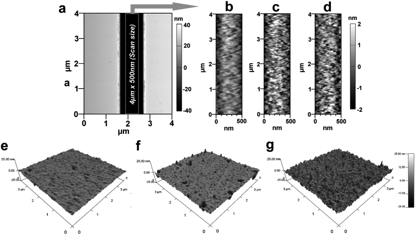 | ||
| Fig. 3 AFM characterization of a PMMA nanofluidic device with 1 μm × 50 nm nanoslit (a) for: (b) u-PMMA; (c) O2-PMMA; and (d) NH2-PMMA. The image shown is 4 μm × 500 nm. The measured root-mean-square (RMS) surface roughness was 0.80 nm, 0.95 nm and 1.03 nm, respectively, for these three devices. Also shown are AFM images for planar PMMA; (e) u-PMMA (f) O2-PMMA and (g) NH2-PMMA. Images on the planar PMMA were scanned over an area of 3.5 × 3.5 μm. | ||
Surface charge and pH effects
As shown in Fig. S6,† the nanofluidic device was comprised of input/output microchannels interconnected by an array of nanochannels with the majority of the voltage drop occurring across the nanochannels (see Table S1† for resistance values of the fluidic network). Therefore, the majority of the electrokinetic flow occurred within the nanochannels, which can be heavily influenced by surface charge and λD to name a few. The surface charge can be a significant determinant of the fluid dynamics for devices possessing high surface-to-volume ratios. Depending on the solution pH and the surface chemistry, the solid can have either a positive or negative surface charge density, σs, described by ; where qi = zie and qi is the net charge of ion i, zi is the valency of ion i, e is the electron charge, and A is the surface area; this can be used to compute the number of charged sites per unit area, Γ in nm−2.66 Due to wall surface charge, an EDL develops to maintain the electroneutrality at the solid–liquid interface.67 For a channel filled with a symmetrical 1:1 electrolyte such as KCl with ionic concentration c, the EDL thickness or λD is;
 | (1) |
Electrical conductance measurements across nanofluidic channels filled with ionic salt solutions have been used to deduce the magnitude of the surface charge density. Here, we present a modified electrokinetic model based on the report from Stein et al.28 for determining σs. When an external electric field is applied across a nanochannel filled with an ionic salt solution, the measured electrical conductance (GT) is the sum of the bulk conductance (GB) and the surface conductance (GS). At high salt concentrations, the surface charges in the nanochannel are shielded by the mobile ions and have negligible influence on the ion concentration in the nanochannel. In this case, transport is dominated by the ions in the bulk solution and GB depends on the nanochannel dimensions and electrolyte concentration according to;46,55,66
 | (2) |
 | (3) |
Hence, the measured electrical conductance is represented as;
 | (4) |
(Complete derivation of eqn (4) is shown in the SI†). When GB ≈ GS, a transition ion concentration, ct, is observed on a log–log plot of GTversus the ion concentration.55
We investigated the effects of surface modification of polymer nanofluidic devices by experimentally measuring σs of modified PMMA nanoslits and nanochannels by monitoring ionic conductance plots. Fig. 4a and b show the conductance traces for an array of surface modified nanoslits (22 μm × 1 μm × 50 nm) and nanochannels (45 μm × 120 nm × 120 nm) measured over a range of KCl concentrations (10−5 M – 1 M in Tris buffer, pH = 7.8). In both devices, the conductance results obtained before and after surface modification differed essentially in the low ionic concentration regime. This effect was characterized by a shift of the plateau conductance suggesting a change in the surface charge dependent on the nature of the modification. When the modified surfaces were in contact with an electrolyte at pH 7.8, ∼99.9% of the surface carboxyl groups (pKa = 4.66) would be deprotonated and ∼99.0% of the amine groups (pKa = 10.42) would be protonated.69 At extreme pH values and low buffer concentrations, the counterions in solution necessary to maintain electroneutrality are H+ and K+ for O2-PMMA devices and Cl− and OH− for the NH2-PMMA devices. However, at pH 7.8 and KCl concentration ≥10−5 M, [K+] ≫ [H+] and [Cl−] ≫ [OH−]. Therefore in eqn (4) (and eqn (S11)†), μopp ≈ μK+ or μCl− for the deprotonated and protonated carboxyl and amine surfaces, respectively.70
 | ||
| Fig. 4 Conductance plots obtained from surface modified devices consisting an array of (a) four nanoslits (each 1 μm wide, 50 nm deep and 22 μm long), and (b) seven nanochannels (each 120 nm wide, 120 nm deep and 45 μm long) square and circle markers represent the data obtained for the plasma and amine modified surfaces, respectively. The solid blue line represents the trace of the theoretical bulk conductance calculated with eqn (2). Each data point represents an average of five measurements with a scatter in the data within 5–8% of the mean value. From the graph, the effective surface charge density as calculated from the transition concentration, ct, was 38.2 mC m−2 for plasma treated nanoslit, 28.4 mC m−2 for amine treated nanoslit, 40.5 mC m−2 for plasma treated nanochannel and 22.9 mC m−2 for the amine treated nanochannel. | ||
At a KCl concentration greater than 10−2 M, the measured ionic conductance in both the nanoslits and nanochannels fit linearly to the theoretical bulk conductance (Fig. 4) and was reproducible from one device to another. This confirmed that there was no significant change in the dimensions of the fluidic channels during thermal embossing, device assembly and surface chemical modification. However, at low electrolyte concentrations (surface charge-governed regime), the nanochannel conductance deviated from linearity and plateaued for both the plasma and amine treated devices with the measured surface conductance lower for the –NH3+ terminated devices compared to the –COO− terminated devices. For the nanoslit devices, the average surface conductance at this region was 7.5 × 10⁻¹⁰ S for the O2-PMMA device. After amination, the conductance dropped to 3.8 × 10⁻¹⁰ S, ∼50.7% of its original value (Fig. 4a). The transition concentration, ct, used to compute σs was approximately 6.60 mM and 3.52 mM for the O2- and NH2-PMMA surfaces, respectively. For O2-PMMA nanoslits, we obtained |σs| ∼ 38.2 mC m−2, which was less than 60 mC m−2 reported by Stein et al.28 and 214 mC m−2 reported by Schoch et al.55 for glass-based nanoslits measured at pH 8. For the NH2-PMMA nanoslit, |σs| was 28.4 mC m−2. In the nanochannels, the conductance in the low ionic strength region for the amine-modified device dropped to ∼67.6% of its O2-PMMA device. The surface charge densities were 40.5 mC m−2 and 22.9 mC m−2 for the O2- and NH2-PMMA devices, respectively (Fig. 4b).
We also monitored the effect of pH on σs of PMMA nanoslits and nanochannels. As depicted in Fig. 5, the plasma modified nanoslits and nanochannels indicated that the surface charge density gradually increased as the pH of the electrolyte solution increased because at low pH the surface carboxyl groups were converted to their protonated form. This leads to a corresponding decrease in the surface conductance as less counterions are attracted into the fluidic channel. At high pH, the carboxyl groups become deprotonated thereby increasing σs. An opposite trend was observed for the amine modified surfaces. The measured surface conductance was higher at low pH and lower at high pH. This is most likely due to the conversion of the –NH2 groups to –NH3+ groups at low pH. At pH ≥8, the surfaces of the O2-PMMA devices were fully deprotonated and the |σs| for the nanochannel was found to be greater than the nanoslits. The values were 38.3 mC m−2 (Γ ≈ 4.2 nm−2) and 40.5 mC m−2 (Γ ≈ 4.0 nm−2) for the fully deprotonated PMMA nanoslit and nanochannel, respectively. These values were found to remain relatively constant at pH > 10. In the nanochannel, the width is comparable to the height, therefore, the surface charge density of the vertical walls, which is typically neglected in the nanoslit, also contributes to the ion transport within the channel.71 Surplus counterions would be attracted into the nanochannel and more coions would be excluded.
 | ||
| Fig. 5 Plot showing the effect of pH on the surface charge density σs, in plasma and amine modified nanoslits and nanochannels. | ||
EOF measurements
The EOF can be described in terms of a mobility, μeof = υeof/E, where υeof is the steady-state bulk EOF. At low λD, μeof can be represented in terms of the bulk solvent viscosity ηo, and the zeta potential ζ by the Helmholtz-Smoluchowski relation:72 | (5) |
Also, the zeta potential can be represented in terms of σs and λD for different electrolyte solutions by combining eqn S(9) into (10) in Chai et al.†:42
 | (6) |
With ε0 and εr constants, conditions that change σs, ζ, λD, or ηo will alter the magnitude of the EOF. μeof was measured using the current monitoring method.73 For the EOF measurement, we used PMMA devices possessing a single nanofluidic channel 138 μm long and 0.1 M and 0.05 M KCl solutions to allow for the generation of a large amount of readable current (see Fig. S6c† for a typical current trace) and to ensure that the measurement was performed at a region where eqn (5) is valid (λD ≤ 2 nm). This single channel geometry eliminates errors in migration time that may arise due to preferential filling across an array of nanochannels during electrolyte replacement. A negative EOF value indicated that the EOF was from cathode to anode and consistent with a positively charged fluidic channel wall while a positive EOF value indicated a negatively charged wall. Molecular Dynamics (MD) simulations reported by Qiao et al.70 have revealed that differences in the distribution of counterions for negatively charged O2-PMMA devices when compared to the positively charged NH2-PMMA is influenced by the finite size of the ions – K+ (0.27 nm) and Cl− (0.36 nm) and the EOF is influenced by surface fluid interactions.
In previous work, we have shown that exposing PMMA microchannels to controlled plasma conditions can generate carboxylate groups with a surface coverage of 2.7 ± 0.5 × 10⁻⁹ mol cm−2.44 We have also reported the EOF at pH 7.4 for carboxylated and NH2-terminated PMMA microfluidic devices to be 4.43 ± 0.58 × 10⁻⁴ cm2 V−1 s−1 and −1.34 ± 0.21 × 10⁻⁴ cm2 V−1 s−1, respectively.38 As shown in Table 1, we obtained an EOF of 0.93 ± 0.03 × 10⁻⁴ cm2 V−1 s−1 and −0.82 ± 0.01 × 10⁻⁴ cm2 V−1 s−1 for O2- and NH2-PMMA nanoslits, respectively. For the O2- and NH2-PMMA nanochannels, the EOF was found to be 1.02 ± 0.02 × 10⁻⁴ cm2 V−1 s−1 and −0.75 ± 0.02 × 10⁻⁴ cm2 V−1 s−1, respectively. The trend and magnitude of the EOF observed in the PMMA nanofluidic devices scales with the measured σs in the nanochannel and was consistent with molecular dynamic simulations reported by Qiao et al.74 The values reported for the O2-PMMA nanochannels were similar to that reported by Menard et al.17 for fused silica nanochannels (≤100 nm) measured using 2× TBE with 2% polyvinylpyrrolidone acting as an EOF suppressor (0.79 ± 0.01 × 10⁻⁴ cm2 V−1 s−1) and ∼35.8 ± 4.4% lower when compared to fused silica channels measured with 2× TBE only (1.58 ± 0.01 × 10⁻⁴ cm2 V−1 s−1). A possible reason for the lower EOF observed in the PMMA nanofluidic devices is the low ζ. This conclusion is supported by the results from the continuum theory based on the Poisson–Boltzmann equation for the ion distribution, Navier–Stokes equations for fluid transport72 and atomistic simulations.74 Both models showed that the EOF in a nanofluidic channel varies almost linearly with ζ with the latter model true for surface charge densities ≤80 mC m−2.74 Furthermore, ζ depends on the chemistry of the solid–liquid interface and is related to the surface charge density by parameters such as the ionic strength, density of charged sites on the surface, their pKa values and the solution pH, which modulates the extent of dissociation of the surface groups (Fig. 5).
| Device | Terminating groups | σ s (mC m−2) | ζ (mV) | μ eof (cm2 V−1 s−1) × 10−4 | |
|---|---|---|---|---|---|
| Expecteda | Measured | ||||
| a Calculated from eqn (6) using the values for σs and ζ. | |||||
| Nanoslit | O2-PMMA, NH2-PMMA | −38.3, 28.4 | −57.1, 45.8 | 4.53, −3.63 | 0.93 ± 0.025, −0.82 ± 0.012 |
| Nanochannel | O2-PMMA, NH2-PMMA | −40.5, 22.9 | −59.8, 38.3 | 4.74, −3.04 | 1.02 ± 0.017, −0.75 ± 0.021 |
In addition, recent reports have shown that reducing the size of fluidic channels can result in reductions of the EOF due to the apparent increase in the viscosity of a fluid upon confinement in charged nanoconduits,75–78 an effect not considered in eqn (5). In most cases, this phenomenon makes the ratio of the apparent to predicted or bulk viscosity, represented as ηapp/ηo, to exceed 1.3 with this ratio dependent on the material of the channel walls, size and shape of the channel, the ionic concentration, ζ, temperature, and dielectric constant.77 Due to the relatively higher ζ in glass-based devices, ηapp/ηo is expected to be greater when compared to thermoplastic devices. This may explain why the EOF measured in glass nanoslits at pH 8.5 (∼1.3 × 10⁻⁴ cm2 V−1 s−1) was lower than those of fused silica micro-capillaries (5 × 10⁻⁴ cm2 V−1 s−1)79 or glass microchannels (4.82 × 10⁻⁴ cm2 V−1 s−1).80
Transport dynamics of λ-DNA through thermoplastic nanochannels
The majority of applications explored in nanofluidic devices have focused on investigating the transport properties of dsDNA confined in fused silica glass17,81–86 and elastomeric87,88 nanochannels. However, because thermoplastics possess dissimilar surface properties compared to glass-based devices,30 it becomes necessary to explore the transport properties of dsDNA in these devices. Although, a few studies have utilized PMMA-based nanoslits32 and nanochannels89,90 for DNA stretching, the electrokinetic parameters of dsDNA in surface modified thermoplastic 2D nanochannels is yet to be reported. Understanding the effects of σs and the charge polarity on these parameters and on the stretching properties of dsDNA in thermoplastic nanochannels is necessary for assessing the viability of these devices for applications in DNA sizing or mapping.First, we assessed the degree of extension of dsDNA confined in O2-PMMA nanochannels seeded with 2× TBE buffer (pH 7.5). When a DNA molecule with width w was driven from a microchannel into the nanochannel under a constant field, upon initial entrance (also called DNA injection), the molecule was observed to stretch because the pulling electric force acted against the resistance due to the entropic interface and frictional forces experienced by the portion of the molecule resident in the microchannel (red trace and insert in Fig. 6a).86 When the field was turned off after the molecule had fully entered the nanochannel, the molecule underwent elastic relaxation and attained an equilibrium extension length shorter than the injection length (blue trace and insert of Fig. 6a). Assuming that the nanochannel has a depth D, which is less than the free-solution radius of gyration but greater than the persistence length lp of the molecule, due to self-avoidance the confined molecule will extend in such a way that it divides into a series of non-interpenetrating blobs with the molecular mass distributed along the channel with relatively uniform density.83 We estimated the extension factor ε of the confined DNA molecule possessing an equilibrium extension length LE and a contour length LC with the equation;
 | (7) |
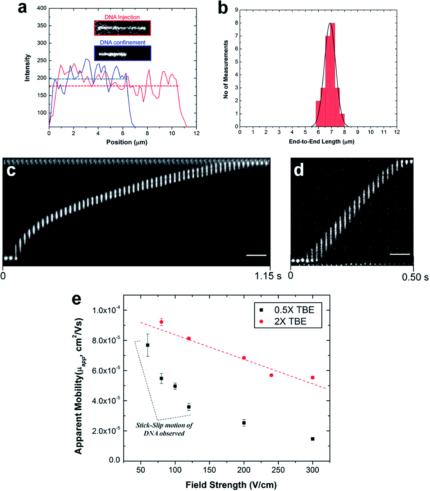 | ||
| Fig. 6 (a) Representative fluorescence intensity profile of an individual YOYO-1 stained λ-DNA molecule after injection (red line) and confinement (blue line) in the plasma modified nanochannel filled with 2× TBE buffer. Complete injection into the nanochannel produced an initial molecule length of 11.25 ± 1.68 μm (calculated from n = 20 events). However, when the voltage was turned off, the DNA relaxed to its equilibrium length. (b) Histogram of the measured end-to-end length of relaxed λ-DNA molecules confined in the PMMA nanochannel. The average equilibrium length determined by the Gaussian curve fit (black line) was ∼6.88 ± 0.43 μm. Representative frames of fluorescently stained λ-DNA molecules translocating through a 100 nm × 100 nm plasma modified PMMA nanochannel and imaged in (c) 0.5× and (d) 2× TBE buffer at 80 V cm−1 and 120 V cm−1, respectively. The time between frames is approximately 20 ms and scale bars are 10 μm. (e) Plots of DNA apparent mobility against the electric field strength for DNA translocation through the single nanochannel filled with 0.5× (black markers) and 2× (red markers) TBE buffer. Error bars represent the standard deviations in the measurements (n = 10). | ||
Although, the total contour length of an unstained λ-DNA molecule (48.5 kbp) is 16.3 μm, at our intercalating dye concentration, we expect a 23% increase in length to 20 μm.82 Therefore, from eqn (7), we expect the extension factor for a stained λ-DNA molecule with a width of 3 nm (ref. 91) and persistence length of 50 nm confined in a 100 × 100 nm nanochannel to be ∼0.25. Nevertheless, we note that eqn (7) does not account for ionic effects, like the buffer ionic strength and viscosity, on DNA elasticity and wall wettability, roughness and frictional drag on the overall extension of the DNA molecule.81,92,93
In our experiment, we observed that when stained λ-DNA molecules were completely introduced into the O2-PMMA nanochannels, it stretched to ∼11.25 ± 1.68 μm at initial entry (calculated from n = 20). When the field was turned off, the DNA molecules remained confined in the nanochannel but relaxed to an overall average extension length of 6.88 μm, determined from a Gaussian curve fit of the histogram shown in Fig. 6b. The experimental extension factor was 0.34, a value ∼40% greater than that predicted by the de Gennes theory. The enhanced stretching of the confined DNA molecule was likely due to additional interfacial surface forces in the form of surface energy acting on the DNA molecule from the charged nanochannel walls. The measured surface energy for O2-PMMA devices was ∼38.9 mJ m−2 (see Fig. S3 in ESI†).
Next, we investigated the electrophoretic properties of DNA molecules electrokinetically driven through nanochannels using 50 μm long, 100 nm × 100 nm channels. All DNA movements represented in the frames shown in Fig. 6c and d were observed without the need of an EOF suppressor. The apparent electrophoretic mobility μapp of DNA in the nanochannel was due to the electrophoretic mobility of DNA, μep, and the EOF.
Fig. 6e shows the variation of μapp for λ-DNA traveling through O2-PMMA nanochannels filled with 0.5× (black squares) and 2× (red circles) TBE. Our results revealed that the apparent mobility of λ-DNA was lower in the channel filled with 0.5× TBE than that of 2× TBE. One possible reason for this was that as the ionic strength of the buffer solution in the charged nanochannel was reduced, there was a corresponding increase in λD (∼30 nm for 0.5× and ∼8 nm for 2× TBE, estimated from classical theory).94,95 This led to a larger EOF for the lower ionic strength buffer thereby reducing μapp of λ-DNA molecules through the nanochannel. We observed that in the devices filled with 2× TBE, the DNA moved through the nanochannel with a constant velocity (Fig. 6d) and an almost linear variation of the electrophoretic mobility for the entire range of electric field strengths studied (red trace in Fig. 6e). This confirmed the absence of dielectrophoretic trapping sites along the channel wall, which was supported by the low nanochannel wall roughness. Interestingly, in the nanochannels seeded with 0.5× TBE, we observed intermittent (stick–slip) motion of the DNA molecules through the nanochannel similar to previous reports32,84 at measurements performed <150 V cm−1 (Fig. 6c). Based on MD simulations96 and theoretical computations,97 a highly negatively charged DNA molecule translocating through a nanochannel interacts both electrically (attractive or repulsive forces) and hydrodynamically with the channel wall. Therefore, we attributed the intermittent motion of DNA to latent electrical interactions between the charged DNA molecule and the thick EDL and this presents the possibility that at this field strength, the driving force was less than the interfacial force. This observation is yet to be reported for DNAs translocating through glass nanofluidic devices at this field strength because the threshold field strength required to introduce DNA into nanochannels without the addition of an EOF suppressor was >200 V cm−1 for 100 nm nanochannels.17 However, at field strengths greater than 200 V cm−1, we did not observe intermittent motion of DNA in these devices with 0.5× TBE. It is possible that at these fields, the driving force overwhelmed the interfacial force causing the DNA to move through the nanochannel with continuous velocity or that the wall interactions occurred so fast they were not detectable at our imaging frame rate.
Finally, we performed translocation experiments in a NH2-PMMA device using 2× TBE (pH 7.4). At this pH, we observed that λ-DNA adsorbed onto the surface of the assess microchannels and remained immobile even with the application of a large bias voltage. This sticking is probably due to strong electrostatic interactions between the negatively charged DNA backbone and the positively charged amine groups. When the solution pH was increased to 10, there were significant reductions in DNA sticking in the microchannel and several λ-DNA molecules were observed to move towards the entrance of the nanochannel. However, when the DC voltage was turned on, the DNA molecules initially attempted to enter the nanochannel but paused at first entry (Fig. S7 in ESI†). No further movement was observed at higher fields and even with reversed DC voltages. This is likely due to strong wall interactions with residual –NH3+ groups or hydrogen bonding between the DNA and the deprotonated –NH2 groups overwhelming the electrokinetic driving force.
Conclusions
In this work, we report a simple and robust fabrication strategy that can be used to produce thermoplastic nanofluidic devices with structures below 20 nm. Furthermore, because the fabrication steps were successfully achieved using simple bench top UV curing and thermal embossing instruments, the cost of device fabrication was significantly reduced compared to conventional NIL techniques. We demonstrated the successful modification of thermoplastic nanoslits and nanochannels using oxygen plasma to produce carboxylic acid moieties that could be subsequently converted into amino groups by reaction with EDA. For the conditions reported in this work, the plasma treated polymer nanoslits and nanochannels were observed to possess |σs| of 38.2 mC m−2 and 40.5 mC m−2, respectively, at pH 7.8. These values were lower than that reported for their glass-based counterparts. The low surface charge densities in polymer nanofluidic devices helped to minimize artifacts arising from ion exclusion due to concentration polarization. The ability to generate positively charged moieties in a simple modification scheme with |σs| of 28.4 mC m−2 in the nanoslits and 22.9 mC m−2 in the nanochannels offers a unique venue for performing nanochannel chromatography by generating the proper stationary phase.The reduced EOF observed in PMMA nanofluidic devices compared to polymer microchannels and glass nanochannels was likely due to lower surface charge density (and zeta potential) and apparent increases in fluid viscosity due to nanoconfinement. Generally, lower EOF values are desirable in applications involving DNA analysis for mapping and sequencing because it enables the introduction of these biomolecules into the fluidic channels without the need for EOF suppressors.
Acknowledgements
The authors would like to thank National Institute of Health (NIH R21HG006278) and the National Science Foundation (CBET-1067583) for supporting this work. We also acknowledge Dr C. Donley of the UNC Chapel Hill Analytical and Nanofabrication Laboratory for assistance with the XPS data, Dr A. S. Kumbhar for acquiring the AFM, UNIST Central Research Facility (UCRF) South Korea for assistance with ATR-FTIR, Dr H. Wang for helpful discussions and the UNC-Olympus Imaging Research Center.References
- J. W. van Honschoten, N. Brunets and N. R. Tas, Chem. Soc. Rev., 2010, 39, 1096–1114 RSC.
- R. K. Anand, E. Sheridan, K. N. Knust and R. M. Crooks, Anal. Chem., 2011, 83, 2351–2358 CrossRef CAS PubMed.
- A. Mani, T. A. Zangle and J. G. Santiago, Langmuir, 2009, 25, 3898–3908 CrossRef CAS PubMed.
- Y.-C. Wang, A. L. Stevens and J. Han, Anal. Chem., 2005, 77, 4293–4299 CrossRef CAS PubMed.
- S. J. Kim, Y.-C. Wang, J. H. Lee, H. Jang and J. Han, Phys. Rev. Lett., 2007, 99, 044501 CrossRef PubMed.
- S. J. Kim, L. D. Li and J. Han, Langmuir, 2009, 25, 7759–7765 CrossRef CAS PubMed.
- Q. Pu, J. Yun, H. Temkin and S. Liu, Nano Lett., 2004, 4, 1099–1103 CrossRef CAS.
- H. Craighead, Nature, 2006, 442, 387–393 CrossRef CAS PubMed.
- H. G. Craighead, J. Vac. Sci. Technol., A, 2003, 21, S216–S221 CAS.
- O. A. Saleh and L. L. Sohn, Nano Lett., 2003, 3, 37–38 CrossRef CAS.
- L. D. Menard, C. E. Mair, M. E. Woodson, J. P. Alarie and J. M. Ramsey, ACS Nano, 2012, 6, 9087–9094 CrossRef CAS PubMed.
- T. A. Zangle, A. Mani and J. G. Santiago, Chem. Soc. Rev., 2010, 39, 1014–1035 RSC.
- A. Piruska, M. Gong, J. V. Sweedler and P. W. Bohn, Chem. Soc. Rev., 2010, 39, 1060–1072 RSC.
- T. Tsukahara, K. Mawatari and T. Kitamori, Chem. Soc. Rev., 2010, 39, 1000–1013 RSC.
- U. F. Keyser, S. van Dorp and S. G. Lemay, Chem. Soc. Rev., 2010, 39, 939–947 RSC.
- S. Pennathur, F. Baldessari, J. G. Santiago, M. G. Kattah, J. B. Steinman and P. J. Utz, Anal. Chem., 2007, 79, 8316–8322 CrossRef CAS PubMed.
- L. D. Menard and J. M. Ramsey, Anal. Chem., 2013, 85, 1146–1153 CrossRef CAS PubMed.
- S. J. Kim, S. H. Ko, K. H. Kang and J. Han, Nat. Nanotechnol., 2013, 8, 609 CrossRef CAS.
- L.-J. Cheng and L. J. Guo, Chem. Soc. Rev., 2010, 39, 923–938 RSC.
- F. Persson and J. O. Tegenfeldt, Chem. Soc. Rev., 2010, 39, 985–999 RSC.
- S. L. Levy and H. G. Craighead, Chem. Soc. Rev., 2010, 39, 1133–1152 RSC.
- X. Liang and S. Y. Chou, Nano Lett., 2008, 8, 1472–1476 CrossRef CAS PubMed.
- C. H. Reccius, J. T. Mannion, J. D. Cross and H. G. Craighead, Phys. Rev. Lett., 2005, 95, 268101 CrossRef PubMed.
- S. L. Levy, J. T. Mannion, J. Cheng, C. H. Reccius and H. G. Craighead, Nano Lett., 2008, 8, 3839–3844 CrossRef CAS PubMed.
- H. Daiguji, Chem. Soc. Rev., 2010, 39, 901–911 RSC.
- J. Han and H. G. Craighead, Science, 2000, 288, 1026–1029 CrossRef CAS PubMed.
- A. Plecis, R. B. Schoch and P. Renaud, Nano Lett., 2005, 5, 1147–1155 CrossRef CAS PubMed.
- D. Stein, M. Kruithof and C. Dekker, Phys. Rev. Lett., 2004, 93, 035901 CrossRef PubMed.
- R. Karnik, K. Castelino, R. Fan, P. Yang and A. Majumdar, Nano Lett., 2005, 5, 1638–1642 CrossRef CAS PubMed.
- R. Chantiwas, S. Park, S. A. Soper, B. C. Kim, S. Takayama, V. Sunkara, H. Hwang and Y.-K. Cho, Chem. Soc. Rev., 2011, 40, 3677–3702 RSC.
- S. Y. Chou, P. R. Krauss and P. J. Renstrom, Appl. Phys. Lett., 1995, 67, 3114–3116 CrossRef CAS.
- R. Chantiwas, M. L. Hupert, S. R. Pullagurla, S. Balamurugan, J. Tamarit-Lopez, S. Park, P. Datta, J. Goettert, Y.-K. Cho and S. A. Soper, Lab Chip, 2010, 10, 3255–3264 RSC.
- J. Wu, R. Chantiwas, A. Amirsadeghi, S. A. Soper and S. Park, Lab Chip, 2011, 11, 2984–2989 RSC.
- P. Abgrall, L.-N. Low and N.-T. Nguyen, Lab Chip, 2007, 7, 520–522 RSC.
- O. Rotting, W. Ropke, H. Becker and C. Gartner, Microsyst. Technol., 2002, 8, 32–36 CrossRef CAS.
- S. A. Soper, A. C. Henry, B. Vaidya, M. Galloway, M. Wabuyele and R. L. McCarley, Anal. Chim. Acta, 2002, 470, 87–99 CrossRef CAS.
- S. B. Hawthorne, Y. Yang, C. B. Grabanski, D. J. Miller and M. L. Lee, Anal. Chem., 2000, 72, 642–643 CrossRef CAS.
- S. L. Llopis, J. Osiri and S. A. Soper, Electrophoresis, 2007, 28, 984–993 CrossRef CAS PubMed.
- J. M. Jackson, M. A. Witek, M. L. Hupert, C. Brady, S. Pullagurla, J. Kamande, R. D. Aufforth, C. J. Tignanelli, R. J. Torphy, J. J. Yeh and S. A. Soper, Lab Chip, 2014, 14, 106–117 RSC.
- A. C. Henry, T. J. Tutt, M. Galloway, Y. Y. Davidson, C. S. McWhorter, S. A. Soper and R. L. McCarley, Anal. Chem., 2000, 72, 5331–5337 CrossRef CAS PubMed.
- C. M. Chan, T. M. Ko and H. Hiraoka, Surf. Sci. Rep., 1996, 24, 1–54 CrossRef CAS.
- J. Chai, F. Lu, B. Li and D. Y. Kwok, Langmuir, 2004, 20, 10919–10927 CrossRef CAS PubMed.
- S. Wei, B. Vaidya, A. B. Patel, S. A. Soper and R. L. McCarley, J. Phys. Chem. B, 2005, 109, 16988–16996 CrossRef CAS PubMed.
- F. Xu, P. Datta, H. Wang, S. Gurung, M. Hashimoto, S. Wei, J. Goettert, R. L. McCarley and S. A. Soper, Anal. Chem., 2007, 79, 9007–9013 CrossRef CAS PubMed.
- S. C. Yang, Microfluid. Nanofluid., 2006, 2, 501–511 CrossRef CAS.
- D. C. Martins, V. Chu and J. P. Conde, Biomicrofluidics, 2013, 7(1–21), 034111 CrossRef CAS PubMed.
- N. R. Tas, J. W. Berenschot, P. Mela, H. V. Jansen, M. Elwenspoek and A. van den Berg, Nano Lett., 2002, 2, 1031–1032 CrossRef CAS.
- L. D. Menard and J. M. Ramsey, Nano Lett., 2011, 11, 512–517 CrossRef CAS PubMed.
- D. Huh, K. L. Mills, X. Y. Zhu, M. A. Burns, M. D. Thouless and S. Takayama, Nat. Mater., 2007, 6, 424–428 CrossRef CAS PubMed.
- S. Chung, J. H. Lee, M.-W. Moon, J. Han and R. D. Kamm, Adv. Mater., 2008, 20, 3011–3016 CrossRef CAS.
- K. D. Park, S. W. Lee, N. Takama, T. Fujii and B. J. Kim, Microelectron. Eng., 2009, 86, 1385–1388 CrossRef CAS.
- S.-m. Park, Y. S. Huh, H. G. Graighead and D. Erickson, PNAS, 2009, 106, 15549 CrossRef CAS PubMed.
- P. E. Shao, A. van Kan, L. P. Wang, K. Ansari, A. A. Bettiol and F. Watt, Appl. Phys. Lett., 2006, 88(1–3), 093515 CrossRef.
- R. Kwak, S. J. Kim and J. Han, Anal. Chem., 2011, 83, 7348–7355 CrossRef CAS PubMed.
- R. B. Schoch and P. Renaud, Appl. Phys. Lett., 2005, 86, 25311 CrossRef.
- A. Amirsadeghi, J. J. Lee and S. Park, Appl. Surf. Sci., 2011, 258, 1272–1278 CrossRef CAS.
- M. B. Chan-Park, Y. Yan, W. K. Neo, W. Zhou, J. Zhang and C. Y. Yue, Langmuir, 2003, 19, 4371–4380 CrossRef CAS.
- H. Becker and C. Gärtner, Anal. Bioanal. Chem., 2008, 390, 89–111 CrossRef CAS PubMed.
- R. J. Messinger and T. M. Squires, Phys. Rev. Lett., 2010, 105(1–4), 144505 Search PubMed.
- A. S. Ziarani and A. A. Mohamad, Nanoscale Microscale Thermophys. Eng., 2008, 12, 154–169 CrossRef CAS.
- H. M. Park and H. D. Lee, Int. J. Heat Mass Transfer, 2012, 55, 3295–3306 CrossRef CAS.
- M. Wang, J. Wang and S. Chen, J. Comput. Phys., 2007, 226, 836–851 CrossRef CAS.
- D. Kim and E. Darve, Phys. Rev. E: Stat., Nonlinear, Soft Matter Phys., 2006, 73, 051203 CrossRef.
- R. N. Wenzel, J. Phys. Colloid Chem., 1949, 53, 1466–1467 CrossRef CAS.
- D. Y. Kwok and A. W. Neumann, Adv. Colloid Interface Sci., 1999, 81, 167–249 CrossRef CAS.
- R. B. Schoch, J. Han and P. Renaud, Rev. Mod. Phys., 2008, 80, 839–883 CrossRef CAS.
- J. Sonnefeld, A. Göbel and W. Vogelsberger, Colloid Polym. Sci., 1995, 273, 926–931 CAS.
- H. Daiguji, P. Yang and A. Majumdar, Nano Lett., 2003, 4, 137–142 CrossRef.
- G. Meisenberg, Principles of medical biochemistry, Mosby Elsevier, Philadelphia, 2006 Search PubMed.
- R. Qiao and N. R. Aluru, Colloids Surf., A, 2005, 267, 103–109 CrossRef CAS.
- S. Bhattacharyya, Z. Zheng and A. Conlisk, J. Fluid Mech., 2005, 540, 247–268 CrossRef CAS.
- G. Slater, F. Tessier and K. Kopecka, in Microengineering in Biotechnology, ed. M. P. Hughes and K. F. Hoettges, Humana Press, 2010, vol. 583, ch. 5, pp. 121–134 Search PubMed.
- X. Huang, M. J. Gordon and R. N. Zare, Anal. Chem., 1988, 60, 1837–1838 CrossRef CAS.
- R. Qiao and N. R. Aluru, Langmuir, 2005, 21, 8972–8977 CrossRef CAS PubMed.
- N. R. Tas, J. Haneveld, H. V. Jansen, M. Elwenspoek and A. van den Berg, Appl. Phys. Lett., 2004, 85, 3274–3276 CrossRef CAS.
- N. Kaji, R. Ogawa, A. Oki, Y. Horiike, M. Tokeshi and Y. Baba, Anal. Bioanal. Chem., 2006, 386, 759–764 CrossRef CAS PubMed.
- M. Wang, C.-C. Chang and R.-J. Yang, J. Chem. Phys., 2010, 132(1–6), 024701 CrossRef PubMed.
- P. Neogi and E. Ruckenstein, J. Colloid Interface Sci., 1981, 79, 159–169 CrossRef CAS.
- T. Hug, N. d. Rooij and U. Staufer, Microfluid. Nanofluid., 2006, 2, 117–124 CrossRef.
- D. Milanova, R. D. Chambers, S. S. Bahga and J. G. Santiago, Electrophoresis, 2012, 33, 3259–3262 CrossRef CAS PubMed.
- J. O. Tegenfeldt, C. Prinz, H. Cao, S. Chou, W. W. Reisner, R. Riehn, Y. M. Wang, E. C. Cox, J. C. Sturm, P. Silberzan and R. H. Austin, PNAS, 2004, 101, 10979–10983 CrossRef CAS PubMed.
- J. T. Mannion, C. H. Reccius, J. D. Cross and H. G. Craighead, Biophys. J., 2006, 90, 4538–4545 CrossRef CAS PubMed.
- B. Chu, JACS, 1983, 105, 5169 CrossRef.
- L. C. Campbell, M. J. Wilkinson, A. Manz, P. Camilleri and C. J. Humphreys, Lab Chip, 2004, 4, 225–229 RSC.
- O. B. Bakajin, T. A. J. Duke, C. F. Chou, S. S. Chan, R. H. Austin and E. C. Cox, Phys. Rev. Lett., 1998, 80, 2737–2740 CrossRef CAS.
- C. H. Reccius, S. M. Stavis, J. T. Mannion, L. P. Walker and H. G. Craighead, Biophys. J., 2008, 95, 273–286 CrossRef CAS PubMed.
- T. Matsuoka, B. C. Kim, J. Huang, N. J. Douville, M. D. Thouless and S. Takayama, Nano Lett., 2012, 12, 6480–6484 CrossRef CAS PubMed.
- E. Angeli, C. Manneschi, L. Repetto, G. Firpo and U. Valbusa, Lab Chip, 2011, 11, 2625–2629 RSC.
- H. T. Lasse, K. Anna and K. Anders, Nanotechnology, 2008, 19, 125301 CrossRef PubMed.
- P. Fanzio, V. Mussi, C. Manneschi, E. Angeli, G. Firpo, L. Repetto and U. Valbusa, Lab Chip, 2011, 11, 2961–2966 RSC.
- J. A. Schellman and D. Stigter, Biopolymers, 1977, 16, 1415–1434 CrossRef CAS PubMed.
- W. Reisner, J. P. Beech, N. B. Larsen, H. Flyvbjerg, A. Kristensen and J. O. Tegenfeldt, Phys. Rev. Lett., 2007, 99, 058302 CrossRef PubMed.
- C. G. Baumann, S. B. Smith, V. A. Bloomfield and C. Bustamante, PNAS, 1997, 94, 6185–6190 CrossRef CAS.
- B. J. Kirby and E. F. Hasselbrink, Electrophoresis, 2004, 25, 187–202 CrossRef CAS PubMed.
- S.-S. Hsieh, H.-C. Lin and C.-Y. Lin, Colloid Polym. Sci., 2006, 284, 1275–1286 CAS.
- B. Luan, A. Afzali, S. Harrer, H. Peng, P. Waggoner, S. Polonsky, G. Stolovitzky and G. Martyna, J. Phys. Chem. B, 2010, 114, 17172–17176 CrossRef CAS PubMed.
- L. Binquan and S. Gustavo, Nanotechnology, 2013, 24, 195702 CrossRef PubMed.
Footnote |
| † Electronic supplementary information (ESI) available: Surface energy determinations; XPS/FTIR characterization of modified PMMA surfaces; electrical model of nanofluidic device; conductance determinations in nanochannels; DNA translocation through EDA-modified PMMA nanochannels. See DOI: 10.1039/c4an01439a |
| This journal is © The Royal Society of Chemistry 2015 |