
 Open Access Article
 This Open Access Article is licensed under a Creative Commons Attribution-Non Commercial 3.0 Unported Licence
Spatial imaging of carbon reactivity centers in Pd/C catalytic systems†
E. O.
Pentsak
a,
A. S.
Kashin
a,
M. V.
Polynski
ab,
K. O.
Kvashnina
c,
P.
Glatzel
c and
V. P.
Ananikov
*ad
aZelinsky Institute of Organic Chemistry, Russian Academy of Sciences, Leninsky Prospect 47, Moscow, 119991, Russia. E-mail: val@ioc.ac.ru
bFaculty of Chemistry, Moscow State University, Leninskiye Gory, Moscow, 119991, Russia
cESRF - The European Synchrotron, 71 avenue des Martyrs, 38000 Grenoble, France
dDepartment of Chemistry, Saint Petersburg State University, Stary Petergof, 198504, Russia
First published on 8th May 2015
Abstract
Gaining insight into Pd/C catalytic systems aimed at locating reactive centers on carbon surfaces, revealing their properties and estimating the number of reactive centers presents a challenging problem. In the present study state-of-the-art experimental techniques involving ultra high resolution SEM/STEM microscopy (1 Å resolution), high brilliance X-ray absorption spectroscopy and theoretical calculations on truly nanoscale systems were utilized to reveal the role of carbon centers in the formation and nature of Pd/C catalytic materials. Generation of Pd clusters in solution from the easily available Pd2dba3 precursor and the unique reactivity of the Pd clusters opened an excellent opportunity to develop an efficient procedure for the imaging of a carbon surface. Defect sites and reactivity centers of a carbon surface were mapped in three-dimensional space with high resolution and excellent contrast using a user-friendly nanoscale imaging procedure. The proposed imaging approach takes advantage of the specific interactions of reactive carbon centers with Pd clusters, which allows spatial information about chemical reactivity across the Pd/C system to be obtained using a microscopy technique. Mapping the reactivity centers with Pd markers provided unique information about the reactivity of the graphene layers and showed that >2000 reactive centers can be located per 1 μm2 of the surface area of the carbon material. A computational study at a PBE-D3-GPW level differentiated the relative affinity of the Pd2 species to the reactive centers of graphene. These findings emphasized the spatial complexity of the carbon material at the nanoscale and indicated the importance of the surface defect nature, which exhibited substantial gradients and variations across the surface area. The findings show the crucial role of the structure of the carbon support, which governs the formation of Pd/C systems and their catalytic activity.
Introduction
Supported Pd/C systems are ubiquitously used in research and industry as classical catalysts of monumental practical importance for carrying out synthetic transformations.1 In spite of their outstanding role in catalysis and organic synthesis, a mechanistic picture at an atomic scale and insight into their reactivity are still to be accomplished – these questions have been intriguing researchers for many years. Of particular challenge is the atomic-scale mechanism for the formation of Pd/C systems and the spatial imaging of carbon reactivity centers (i.e. the location and characterization of the carbon reactivity centers in 3-D space).Imaging is a powerful technique for revealing the structure and morphology of an object by constructing a visual representation of the object. The excellent ability of imaging to reveal structural features has led to outstanding applications of imaging in biology, chemistry and physics.2–4 Ultrasound, magnetic resonance and X-ray (tomography) imaging are the leading and most widely used diagnostic and analytical tools in medicine, nanotechnology, materials science, catalysis and many other areas. The range of the studied systems varies from the human body to micro-, nano- and sub-nanosized objects, such as cells, nanoparticles and individual atoms.5–8 Typically, to create an image that reflects the scanned area of interest of an object, the object is irradiated with radiation of a specific wavelength and the corresponding physical response is recorded.
Detailed investigation of the unique structure and properties of metal–carbon systems is currently a challenging task. Nano-scale imaging that combines Raman spectroscopy and microscopy is particularly useful for characterizing carbon systems.9 Spatial imaging techniques have been applied to visualize structural information, physical parameters, chemical bonding and electronic properties and to map surface morphologies.10,11 Knowledge of these features is necessary for developing practical applications of graphene.12–14 Determining edge/crystal orientations, measuring stacking orders, revealing atomic lattice and topological defects and mapping the three-dimensional (3-D) structures of composite materials are just a few representative examples of how structural imaging is applied to graphene systems.15–19 Structural studies have revealed the existence of non-uniform reactivity patterns on the surfaces, edges and defect locations of graphene.20,21 Several types of defects increase the reactivity and enable new applications of graphene.20–23 Locations that contain a single vacancy, multiple vacancies, Stone–Wales defects, substitutional impurities, dislocations or grain boundaries are of particular importance.
Reconstructed defects (for example, reconstructed multiple vacancies, Stone–Wales defects and substitutional impurities) induce local changes in the π-electron density and enhance the chemical reactivity of certain graphene sites.24,25 The additional attachment of functional groups to vacancy-type defects can be easily realized.26
Grain boundaries27 and zigzag edges28 possess unique reactivity patterns that result from areas of locally modulated electron density. Reconstructed vacancy defects are important for incorporating additional species (e.g., metal atoms) into the graphene lattice.29
Dramatic variations in the reactivity at different spatial locations in graphene provide fascinating opportunities for the development of new technological materials with a wide range of applications for catalysis, medicine and electronics, among other topics. However, achieving this goal requires direct, detailed imaging of the reactivity of graphene and rational design of functional active sites. As discussed above, several techniques are available for imaging and obtaining information about the structure of graphene, whereas imaging of the reactivity remains a challenge.
Here, we present a new and efficient approach for the spatial imaging of the reactivity of graphene layers on a carbon surface using Pd nanoparticles as a contrast agent. The chemical imaging of graphene layers was successfully realized in 3-D space, thereby enabling the mapping and visualization of localized reactivity patterns. The procedure developed for the spatial imaging of the reactivity of graphene layers permits the detection and visualization of various types of defect sites. It is important to emphasize that the detected sites are classified according to their reactivity rather than their morphology or composition. Analysis of the morphology and composition is accessible using standard structural imaging techniques, however the visualization of reactivity is a challenge.
As the necessary theoretical base to this work, recent computational studies have shown that trapping metal atoms on the defect sites of graphene and doped graphene is a feasible process and the unbinding is strongly thermodynamically unfavourable.20,30–35 The binding of metal particles to the defect sites of carbon surfaces was observed experimentally and is in agreement with the computational predictions.29, 36–40
The unique reactivity of Pd clusters, revealed in the present study, provided a convenient procedure to carry out the practical imaging procedure. Pd clusters were found as excellent markers of reactivity centers with a high contrast in microscopic detection (contrast agent). The overall picture of the metal–carbon interactions revealed in the present study provides a unique insight into the formation and nature of the well-known Pd/C catalytic system.
Results and discussion
Recently, we have demonstrated that Pd2 species stabilized with weakly coordinated dibenzylideneacetone (dba) ligands exhibit fluxional behavior in solution; this behavior results in the generation of Pd clusters and nanoparticles (NPs) under mild conditions.41In the present study, we investigated the interaction of Pd clusters with a carbon surface and revealed that palladium species generated in a solution of Pd2dba3 preferentially attach to the chemically reactive sites of the carbon surface. The key result of the present study was a demonstration of the ability to separate localized areas in graphene layers according to variations in the activity of specific sites.
The dissolution of Pd2dba3 in chloroform afforded a dark red solution, in which the Pd clusters may be generated at 40 °C. The addition of a carbon material with graphene layers led to a rapid reaction with the Pd centers and the complete consumption of the Pd2dba3 from the solution. The reaction can be easily monitored as the solution changes from dark red to colorless (Fig. 1a and b). Nuclear magnetic resonance (NMR) spectroscopy clearly revealed a decrease in the Pd2dba3 concentration in the solution and the release of free uncoordinated dba ligands while the solution was stirred at 40 °C (Fig. 1c). Generation of the Pd seeds and growth of the Pd clusters was followed by their attachment to the carbon surface (Fig. 2a). Field-emission scanning electron microscopy (FE-SEM) observations revealed that Pd clusters were attached to the carbon surface in a specific order (Fig. 2b and c). High resolution STEM study characterized individual metal nanoparticles (Fig. 2d) formed upon metal attachment from the Pd2dba3 molecular precursor (Fig. 2e). In particular, the interaction of the Pd clusters with the graphene layers resulted in the coverage of the carbon surfaces by Pd NPs depending on the degree of chemical activity of the carbon sites (the most reactive carbon sites were covered by Pd NPs first). Consequently, the observed Pd-mapping provided a unique opportunity for the spatial imaging of the chemical reactivity of the graphene layers. The attachment of Pd particles to the carbon surface is a highly thermodynamically favoured process, which proceeds irreversibly under the studied conditions (see also the results of the quantum chemical calculations).
 | ||
| Fig. 1 Monitoring the Pd/C formation process in solution: (a) initial solution of Pd2dba3 in chloroform with the added carbon material; (b) the solution after stirring for 5 h at 40 °C; (c) 1H NMR monitoring of the reaction: blue line – concentration of Pd2dba3, red line – concentration of free dba. | ||
 | ||
| Fig. 2 The developed spatial imaging approach: (a) a schematic image of the initial graphene layers on graphite; (b) a schematic image of the Pd NPs attached to the defect sites at the step edges of the graphene layer; (c) experimental FE-SEM image of the defects mapped with the aid of Pd NPs; (d) STEM image of an individual NP bound to the carbon surface; (e) ball-and-stick model of the Pd2dba3 (tris(dibenzylideneacetone)dipalladium(0) complex). | ||
It was therefore possible to visualize several different reactivity patterns and defect types using the developed approach (Fig. 3). Statistical analysis was done based on 150 samples prepared in this way and more than 1000 microscopy images were recorded. All the images showed clearly visible sets of patterns of nanoparticle allocation, which confirms the reliable reproducibility of the method. In Fig. 3a, there are primarily individual Pd NPs, which are most likely settled onto point defects. This type of detection is suitable for observing single vacancies, Stone–Wales defects, substitutional impurities and adatoms. Fig. 3b shows local accumulations of Pd NPs, which is likely due to the presence of larger defects, such as multiple vacancies, in these areas. The Pd NPs were arranged in short chains on the graphene surface, as shown in Fig. 3c, which indicated the coverage of the linear defects. As shown in Fig. 3d, chains of Pd NPs bordered the grain boundaries, which allowed the individual domains of graphene to be visualized. Fig. 3f shows the chains of Pd NPs that were attached along the carbon surface bends. The observed effect originates from topological defects on the surface of the carbon material. Most of the aforementioned images (Fig. 3a–c and e) contain chains of Pd NPs that helped to map the borders of the graphene sheets. We performed an extensive set of experiments to confirm the wide scope of the developed approach and its applicability to visualize reactivity patterns of many types of graphene-layered structures (see the ESI†).
 | ||
| Fig. 3 Spatial imaging of different types of defects using Pd NPs. Green arrows and blue arrows indicate point defects of different sizes (a and b); red arrows indicate line defects (a, c and e); dashed red lines outline grain boundaries (d); orange arrows indicate the step edges (a–c, and e); and yellow arrows indicate topological defects (f) (see the ESI† for larger images). | ||
The sensitivity to various types of defects and coverage patterns of the reactive sites can be tuned by changing the Pd2dba3 concentration in solution and by varying the amount of carbon material. Increasing the Pd-to-carbon ratio allowed the degree of surface coverage to be controlled (Table 1). With low surface coverage, only the most reactive sites of the carbon surface were mapped (entries 1 and 2; Table 1); with medium surface coverage, further information about carbon sites with high and medium reactivity was obtained (entries 3 and 4; Table 1); high surface coverage provided the complete details about all of the available reactive centers of the carbon surface (entries 5 and 6; Table 1).
| Entry | Pd2dba3·CHCl3, mg | Volume of solvent, ml | Carbon material, mg | Average NP diameter, nm | Coverage of Pd NPs on the carbon surfacea |
|---|---|---|---|---|---|
| a The coverage was measured as the number of NPs per 1 μm2 of surface area; the ranges were roughly classified as low, medium and high coverage with <800 NPs per μm2, 800–2000 NPs per μm2 and >2000 NPs per μm2, respectively. | |||||
| 1 | 0.400 | 5.0 | 100 | 5 ± 2 | Low |
| 2 | 0.500 | 5.0 | 100 | 5 ± 1 | Low |
| 3 | 1.250 | 5.0 | 100 | 8 ± 2 | Medium |
| 4 | 2.500 | 5.0 | 100 | 9 ± 3 | Medium |
| 5 | 5.000 | 5.0 | 100 | 9 ± 3 | High |
| 6 | 10.000 | 5.0 | 100 | 15 ± 3 | High |
| 7 | 1.000 | 5.0 | 200 | 9 ± 3 | Low |
| 8 | 1.000 | 5.0 | 400 | 6 ± 1 | Very low |
| 9 | 1.000 | 5.0 | 100 | 7 ± 2 | Medium |
| 10 | 1.000 | 2.0 | 50 | 6 ± 1 | Medium |
| 11 | 1.000 | 5.0 | 20 | 11 ± 3 | Medium |
| 12 | 0.500 | 1.5 | 15 | 6 ± 1 | Medium |
| 13 | 0.500 | 1.0 | 10 | 7 ± 2 | Medium |
| 14 | 0.025 | 0.5 | 1 | 7 ± 2 | Medium |
Profiling the reactivity of the carbon surface by Pd-mapping was successfully achieved either by changing the amount of Pd2dba3 while keeping the amount of carbon material fixed (entries 1–6) or by changing the amount of carbon material while keeping the amount of Pd2dba3 fixed (entries 7–11).
It is important to note the rather narrow size distribution of the attached NPs that was observed in each experiment. Small variations in the Pd NPs sizes were observed upon changing from the low- to high-coverage mappings.
The optimal conditions for obtaining medium surface coverage included a 40:1 mass ratio of carbon material and Pd2dba3 and stirring at 40°C for 4 h. It is especially important to perform scaling experiments to study the effects of small amounts of carbon material. Indeed, scaling experiments were successfully performed for the entire range of 1–100 mg of carbon material by optimizing the volume of solvent as the key parameter (entries 9–14; Table 1).
In the developed imaging approach, the spatial detection of chemical reactivity was achieved by placing suitable markers, i.e., Pd NPs of an easily detectable size (5–11 nm). The developed procedure resulted in informative images that reflected the distribution of defects and sites of chemical reactivity on the carbon surface. Metal NPs were easily detected with commonly available electron microscopy hardware and provided a nanoscale resolution of the chemical reactivity of the graphene layers.
Varying the concentration of the metal complex in solution and the ratio between the metal and carbon material thus provides a flexible tool for controlling the resolution of and information obtained from the analysis. Aggregate formation did not occur under the optimal conditions, and the number of produced NPs was sufficient for visualizing the patterns of interest.
The unique imaging capabilities of the developed technique were revealed by studying the time dynamics of the Pd-mapping of the carbon surface (Fig. 4). The coverage of the surface of the carbon material by NPs gradually increased until the Pd from the solution was completely consumed (see also Fig. 1). The spatial imaging and mapping of the reactivity were achieved according to the following process: first, single NPs attached to the most-reactive sites on the carbon surface. Then, NPs attached to the less-reactive defect sites on the carbon surface. Finally, chains of NPs formed on the individual graphene layers. Further processing led to greater coverage of the carbon surface and the formation of continuous chains along the edges and domain boundaries. Amazingly, the size of the NPs quickly stabilized and remained almost unchanged during the process (Fig. 4). Such a growth process provides an excellent opportunity for spatially imaging the reactivity centers of a carbon material under simple conditions.

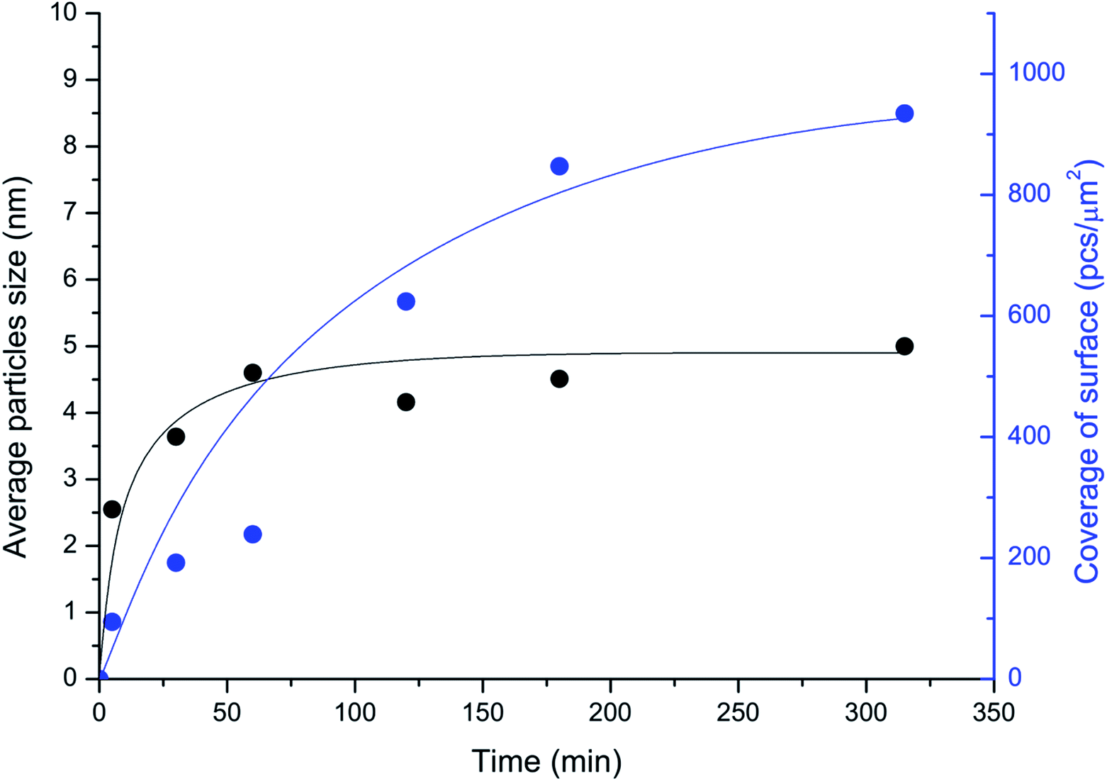 | ||
| Fig. 4 Temporal monitoring of the imaging process: changes in the coverage of the surface of the carbon material (in NPs per μm2; blue curve) and in the sizes of the Pd particles attached to the surface (in nm; black curve); medium coverage conditions were utilized (entry 3; Table 1). | ||
The spatial imaging resolution also depends on the temperature maintained during the mapping of Pd in solution. Smaller-sized NPs (2–3 nm) were observed upon heating the solution at 70 °C, whereas larger particles of 6–7 nm in size were produced at 40 °C. The process was much faster at 70 °C (∼1 min) than at 40 °C (∼4–5 h). Thus, employing a higher temperature during Pd-mapping in solution accelerates the analysis and can increase the resolution. However, at high temperatures, a tendency to form large agglomerates of Pd NPs was observed. The formation of agglomerates reduces the quality of defect visualization; consequently, high temperatures should be used carefully. As a general protocol, we favor a temperature of 40 °C as an optimal balance between imaging resolution and accuracy in the location of reactivity patterns. Mild reaction conditions were important for maintaining the natural state of the sample and avoiding damage to the sample. The carbon defects imaging method described in the present study is perfectly compatible with routinely available hardware for scanning electron microscopy. Regular microscopes allow the easy detection and accurate characterization of particles with sizes about 5–7 nm (Table 1).
For a complete mechanistic picture it is important to understand whether the formation of Pd nanoparticles, which is described above (Fig. 2), involves the growth of small metal clusters. Such atomic scale processes cannot be detected by routine scanning electron microscopy because of insufficient resolution.
A scanning transmission electron microscope (STEM) Hitachi HD-2700 equipped with a CEOS GmbH spherical aberration (Cs) corrector was used for recording the high resolution images. This technique allows SE and STEM images to be recorded with a spatial resolution of 1 Å. Unique insight into the Pd/C sample with a magnification of 2 million times and 5 million times was gained using the aberration corrected scanning electron (SE) images (Fig. 5a and c), as well as high resolution annular dark field (ADF) STEM images (Fig. 5b and d) of the same region. Individual atoms of the Pd nanoparticles can be seen on the ADF STEM images.
 | ||
| Fig. 5 High-resolution images of the Pd NPs attached to the carbon surface: (a) SE image; (b) ADF-STEM image; (c) SE image of the same particles with higher magnification; (d) ADF-STEM image of the same particles with higher magnification. | ||
The study showed that the Pd nanoparticles were concentrated directly at the borders of the carbon layers and their attachment to the edges of the carbon surface can be seen. On the high resolution images, Pd nanoparticles with the sizes of 0.7–2 nm were detected along with larger nanoparticles with sizes of 5–6 nm, which were described above. It can be seen that by increasing the particle size, their shape becomes more regular.
Particles with sizes of 5 nm or more have a regular spherical shape, whereas particles with sizes of less than 2 nm, typically have less symmetrical shape. High resolution EDX-elemental mapping images were recorded to confirm the supposed nature of the observed nanoparticles and of the support (see the ESI, Fig. S25†). It can be seen on EDX-elemental mapping images that the observed nanoparticles are indeed the palladium particles on the carbon sheets.
Data obtained by the HD-2700 microscope allowed the fine details of the structure of the system to be observed, and the high resolution images confirmed our conclusions about the selective attachment of Pd NPs to the edges of the carbon sheets, and revealed the presence of small palladium clusters trapped by the carbon surface (Fig. 2).
The electronic structure of the attached Pd NPs was characterized by recording the X-ray absorption near edge structure (XANES). Pd LIII-edge XANES spectroscopy was employed to determine the chemical state of the palladium on the carbon material.
Palladium was deposited onto the carbon surface from a solution of Pd2dba3 in chloroform at 40 °C. The mapping process was performed until the Pd2dba3 was completely consumed, and the Pd absorption spectra of the resulting carbon material were recorded. To support the analysis, XANES spectra of the prepared sample and of two standard compounds (Pd2dba3·CHCl3 and Pd foil) were recorded (Fig. 6).
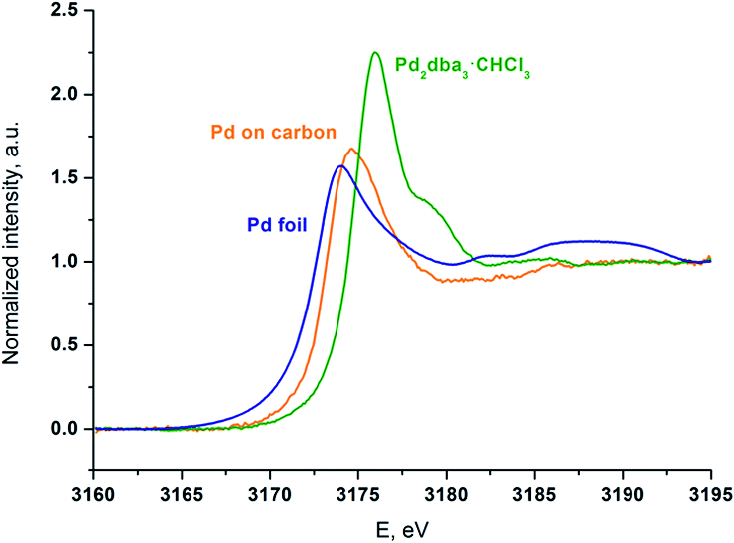 | ||
| Fig. 6 XANES spectra at the Pd LIII edge of the carbon material mapped with palladium NPs (orange line), the initial Pd2dba3·CHCl3 (green line) and Pd foil as a standard sample (blue line). | ||
Although the palladium atoms in both of the standard compounds are considered to be Pd0, there is a notable shift of the white line position in the Pd LIII-edge XANES spectrum of Pd2dba3·CHCl3 compared with that of the Pd foil. Thus, the difference between metallic and coordination compounds can be easily observed.
The positions and shapes of the white (main absorption) lines for the Pd foil and Pd attached to carbon are similar, whereas the peak position of the white line and the overall spectral shape of Pd/carbon are very different from the spectrum of the initial Pd2dba3 compound. The oscillations above the absorption white line that are visible in the Pd foil are washed out in the case of the NPs on the carbon material. This effect indicates a considerable contribution from surface Pd atoms to the spectrum and thus a large surface-to-bulk ratio and the formation of small particles. Most of the Pd atoms were in the metallic state, which is different from those in the Pd2dba3 and bulk Pd foil. The blue shift of the white line of Pd/carbon relative to the Pd foil may have been caused by size effects and interactions with the support.
The results of the synchrotron study revealed that palladium mapping was achieved by the attachment of small metal particles and that Pd2dba3 was largely converted to Pd(0) metallic species during the reaction with the carbon material. The results are in excellent agreement with the NMR and electron microscopy studies discussed above.
A theoretical study was carried out for independent confirmation of the preferable palladium–carbon interactions over specific carbon centers and for an estimation of the relative reactivity of carbon centers in this process. The chemisorption of Pd2 on pristine graphene and defective graphene was modeled by computational methods and several point and 1D defects were considered (see Fig. S26 in the ESI†). Two-layer models of the graphene adsorbent were used, except for the model of the grain boundary defect.
A similar model of the grain boundary defect was proposed in the literature.42 Most computational studies reported to date deal with point defects on graphene. In the present computational study we have addressed the Pd/C system and focused on the experimental findings.
Using spin-polarized computations at the PBE-D3-GPW level of theory we mapped the relative reactivity of Pd2 species towards pristine and defective graphene. Notably, truly nanoscale systems with up to 434 atoms were modeled. The adsorption energies were estimated according to the following formula:
| Eads = EPd2+Gr − (EGr + EPd2) |
The values of adsorption energy predicted in this study are summarized in Fig. 7 (see also Table S1 in the ESI†). As revealed in the computational study, the relative affinity of the Pd2 species to point-defects, 1D-defects and pristine graphene changes in the following order: uncapped armchair edge (armchair-uncapped) > uncapped zigzag edge (zigzag-uncapped) > single vacancy (SV) > double vacancy (DV) > O-terminated zigzag edge (zigzag-O) > H-terminated zigzag edge (zigzag-H) > H-terminated armchair edge (armchair-H) > defect of Stone–Wales type (SW) > grain boundary (GB) > pristine graphene.
 | ||
| Fig. 7 Binding of Pd2 to defect sites of the carbon surface: the ranges of adsorption energy Eads are given in kcal mol−1; palladium atoms are marked by a blue colour and oxygen atoms by a red colour. | ||
The defects with dangling bonds were found to be the most reactive, followed by the DV-defect and then by the O-terminated and H-terminated steps. Next in the sequence were the defects of Stone–Wales type and the grain boundary. The adsorption of Pd2 near the grain boundary is less exothermic compared to the case of point defects (mainly the Stone–Wales-type defect) however the relative exothermicity may be underestimated in this case since a one-layer model of graphene was used. It should also be noted that the number of dangling bonds in the models of uncapped steps with zigzag- and armchair-edges is different (3 and 4 correspondingly), thus making the mutual ordering of this defects model dependent. As we anticipated from the experimental study, Pd2 adsorption on the pristine graphene is the least exothermic. Thus, one may expect that defect sites on graphene or graphite surfaces should be first decorated with Pd species long before the non-defected surface would be able to bind Pd species.
We have also evaluated the possibility of Pd2 binding to small palladium particles. We estimated the adsorption energy of Pd2 on a cub-octahedral Pd79 nanoparticle at the same level of theory (PBE-D3-GPW), and the Eads of the palladium dimer on the nanoparticle was highly exothermic (−123 to −110 kcal mol−1). Thus, if there is enough of the Pd dimer in solution, small palladium nanoparticles undetectable by regular SEM imaging should grow under the experimental conditions until they become clearly visible. Varying the amount of Pd2dba3 and monitoring of the consumption of this complex can be easily done as discussed above.
Several adsorption configurations that had varying values of Eads were found in many cases. These may differ due to different Pd atom positions, for example, adsorption of both Pd atoms on the O-terminated step is much preferred to the case where one Pd atom is bound to an oxygen atom and the other one is located on the pristine surface in close proximity of the step (see Fig. S32 and Table S1 in the ESI†). In the case of Pd2 adsorption near the step with an armchair edge and 4 uncapped carbon atoms, two qualitatively different adsorption structures with Eads of −214 and −175 kcal mol−1 were found. Most favorable was the binding of each Pd atom to two carbon atoms with an unsaturated valence (armchair-uncapped_1, Eads equal to −214 kcal mol−1, line 27 in Table S1†), where a spin-unpolarized system was formed. In the second adsorption complex armchair-uncapped_2 (Eads equal to −175 kcal mol−1, line 28 in Table S1†) one of the carbon atoms (marked with a red circle on Fig. S35†) remained uncapped, thus the adsorption complex remained spin-polarized.
Notably, one of the Pd2-DV-graphene adsorption configurations (DV_2) had a significantly higher absolute adsorption energy (see Fig. S33 and lines 19–23 in Table S1 in the ESI†). This may be attributed to the fact that the DV-defect in that case was reconstructed upon the adsorption, which led to the breaking of the 5–8–5-structure of the defect (compare the marked distances between the two C-atoms involved in the DV-defect in Fig. S33†). A proper sampling of the potential energy surface is suggested when modeling adsorption of transition metal species on defective graphene.
It should be noted that we intended to address the relative reactivity of the defects toward the palladium species studied experimentally. As shown by the calculations, the breaking of the Pd–Pd bond in the Pd2 dimer may occur upon adsorption on the carbon surface. Calculated with the same model and parameters (i.e. at PBE-D3-GPW level of theory), the bond energy in a free Pd2 dimer was 19 kcal mol−1, in good agreement with the experimental values of 20–27 kcal mol−1.43
Defective graphene, as expected, was much more reactive toward Pd2 than the pristine one. The defects with uncapped carbon atoms (armchair-uncapped-, zigzag-uncapped- and SV-defects) were shown to be highly reactive towards the palladium species, as well as DV-defects. Binding to the oxygenated steps on the graphene surface is more favorable than to the H-terminated steps, grain boundaries or defects of Stone–Wales type. The calculated energy parameters for Pd2 attachment to the carbon surface have shown it to be a highly exothermic transformation, which clearly confirms the fundamental basis for the nanoscale imaging procedure, proposed in the present study.
Conclusions
Experimental mapping of the reactivity centers on the surface of the carbon material with Pd markers has indicated that >2000 reactive centers can be individually located per 1 μm2 of surface area. Defects and reactivity centers, which were abundant on the studied carbon surface, are responsible for the assembly of the Pd/C systems and can play a dominant role in catalyst activity and stability under the reaction conditions. This surprising capacity of the graphene layers to accommodate many reactivity centers challenges us to re-examine our understanding of the electronic and structural properties of carbon materials and encourages the development of novel applications.The unique ability of the Pd NPs to attach to carbon sites with locally modified electron densities yields an outstanding tool for mapping the chemical reactivity of carbon centers. We developed a simple, practical procedure in which a carbon material is treated with a solution of a readily available Pd2dba3 complex and a standard electron microscopy image is recorded. The attachment of metal NPs to graphene layers enabled the chemical reactivity of the carbon surface to be visualized with spatial resolution. The key advantages of the developed approach include (i) efficient imaging of nanoscale carbon structures; (ii) high-contrast imaging, which is due to the considerable difference between the studied material (carbon) and imaging probe (Pd); (iii) spatial mapping of the reactivity of the graphene layers, which can be obtained in an arbitrary orientation; and (iv) Pd-mapping of the carbon material under mild conditions at 40 °C without ionizing irradiation, thus avoiding alterations to the properties of the studied sample.
Computational study at a PBE-D3-GPW level revealed the adsorption of Pd2 species to several types of reactivity centers on the carbon surface: armchair-uncapped > zigzag-uncapped > SV > DV > zigzag-O > zigzag-H > armchair-H > SW > GB > pristine graphene. The present study provides an important insight into the formation and structure of Pd/C systems, which represent valuable catalytic materials with widespread applications in organic synthesis. The anticipated development of site-specific binding of metal particles and control over the nature of Pd/C systems will provide new fascinating applications.
Experimental
General methods and materials
Pd2dba3·CHCl3 was synthesized according to the reported procedure.41 Unless otherwise noted, the experiments were conducted in screw-cap glass tubes equipped with a magnetic stir bar.For the FE-SEM measurements the samples were mounted on a 25 mm aluminum specimen stub and fixed with conductive silver paint. The FE-SEM images were processed using the Image Tool software package (the average diameter of the nanoparticles and the degree of surface coverage were measured).
NMR spectra were recorded using a Bruker Avance 600 spectrometer equipped with a 5 mm BBI probe. Data processing was performed with the TOPSPIN software package.
General imaging procedure
Pd2dba3·CHCl3, the carbon material and 5 ml of CHCl3 were placed into the reaction vessel and stirred at 40 °C for 4 h. The solution became colorless after completion of the reaction. The carbon material was separated from the solution by filtration or centrifugation and dried. When necessary, the samples were washed with acetone to remove free dba, which can reduce the quality of SEM images.Electron microscopy images were recorded using a Hitachi SU8000 field-emission scanning electron microscope (FE-SEM). Images were acquired in a secondary electron mode with accelerating voltages of 10, 20 and 30 kV and a working distance of 8–10 mm. About 150 samples were characterized and >1000 images were recorded for a reliable statistical analysis.
NMR monitoring
Pd2dba3·CHCl3 (10 mg), the carbon material (200 mg) and 20 ml of CHCl3 were placed into a 50 ml round-bottom flask equipped with a magnetic stir bar. The reaction mixture was stirred for 5.5 h until the solution became colorless. During the imaging process, 0.5 ml aliquots of the reaction mixture were placed into NMR tubes at specific time intervals. Chloroform was removed from the samples using a nitrogen flow, and 0.6 ml of CDCl3 was added (high-purity Ag-stabilized CDCl3 was used). NMR analysis was performed immediately after sample preparation. The concentrations of Pd2dba3 and free dba were calculated according to a previously reported method.41Imaging at various temperatures
Pd2dba3·CHCl3 (1 mg), the carbon material (10 mg) and 1 ml of CHCl3 were placed into the reaction vessel and stirred at room temperature for 96 h at 40 °C for 4 h or at 70 °C for 1 min until the solution became completely colorless. The carbon material was separated from the suspension using the procedure described above.Scaling procedure
Pd2dba3·CHCl3 (1 mg for entries 9, 10 and 11; 0.5 mg for entries 12 and 13 and 0.025 mg for entry 14 in Table 1), the carbon material (100 mg for entry 9; 50 mg for entry 10; 20 mg for entry 11; 15 mg for entry 12; 10 mg for entry 13 and 1 mg for entry 14 in Table 1) and CHCl3 (5 ml for entries 9 and 11; 2 ml for entry 10; 1.5 ml for entry 12; 1 ml for entry 13 and 0.5 ml for entry 14 in Table 1) were placed into the reaction vessel and stirred at 40 °C (4 h for entries 9–13 and 80 min for entry 14 in Table 1). The carbon material was separated from the suspension using the procedure described above.Time variation
Pd2dba3·CHCl3 (5 mg), the carbon material (500 mg) and 25 ml of CHCl3 were placed into a 50 ml round-bottom flask equipped with a magnetic stir bar. The reaction mixture was stirred for 5.5 h until the solution became colorless. During the imaging process, 2.5 ml aliquots of the reaction mixture were sampled at specific time intervals. The carbon material was filtered, washed with acetone and dried.High resolution images and EDX-elemental mapping
A scanning transmission electron microscope (STEM) instrument Hitachi HD-2700 equipped with a CEOS GmbH spherical aberration (Cs) corrector was utilized for the production of high resolution SE images and STEM images. All images were recorded at an accelerating voltage of 200 kV. The analysis time for the EDX-elemental mapping was 10 minutes.X-Ray spectroscopic studies
X-Ray absorption spectra at the Pd LIII-edge were recorded at beamline ID26 of the European Synchrotron Radiation Facility (ESRF).44,45 The incident beam was selected using the 〈111〉 reflection of a pair of cryogenically cooled Si crystals, which provided an energy bandwidth of 0.45 eV. Higher harmonics were suppressed by three Si mirrors operating in total reflection mode. The spectra were recorded in a total fluorescence yield (TFY) mode using a photodiode. The total flux on the sample was 1013 photons per second with a beam footprint of 200 × 600 μm2 (vertical × horizontal).Computational procedures
The GPW method46 implemented in the CP2k program47 (version 2.6) was used for all the computations presented. Spin-polarized computations were performed in all cases. The dispersion-corrected48 PBE49 functional was used for modeling the Pd2 adsorption on pristine and defective graphene. The cutoff of the finest grid level (5 integration grids were used in all cases) and REL_CUTOFF values of 1000 Ry and 60 Ry, correspondingly, were chosen. In the case of the Pd atoms, the norm-conserving pseudopotentials of Hutter and co-workers50,51 including semi-core states were chosen (GTH-PBE-q18) and the non-linear core corrected pseudopotentials52 were used for the other atoms. A DZVP-MOLOPT-SR-GTH basis set was used in all computations performed.53The electrostatic interactions with periodic images were suppressed in the case of the Pd atom, Pd2, Pd79 and Pd81 in all directions (ref. 54), and in the direction perpendicular to the graphene plane in the case of the graphene and Pd–graphene systems.55
Fermi-Dirac smearing with an electronic temperature of 300 K was used in all calculations except with the isolated Pd2 clusters and the Pd atom, and 300 molecular orbitals were added to allow partial occupancies in all calculations, except the Pd2 and Pd atom cases. The number of unpaired electrons was not fixed for the 2D-periodic systems and was fixed to be an integer number for Pdn (n = 1, 2, 79, 81) systems. The Pd atom and Pd2 cluster were treated as having singlet and triplet spin states correspondingly. A standard diagonalization algorithm with a Broyden mixing scheme was used to solve the Kohn–Sham equations during the geometry optimization runs, and a KS-SCF convergence criterion of 1.0 × 10⁻⁶ Ha was chosen.
The geometry optimizations were performed with the BFGS algorithm, and the convergence criteria were equal to ∼1.1 × 10⁻³ Å, ∼0.5 × 10⁻³ Å, ∼5.7 × 10⁻⁴ Ha × Å−1 and ∼3.8 × 10⁻⁴ Ha × Å−1 for the maximal step size, the RMS step size, the maximum force component and the RMS force respectively. The cell parameters were kept fixed during the geometry optimizations.
Model systems were constructed according to the following procedure. Firstly, rectangular two-layer graphene cells were generated with the C–C-bond length equal to 1.42 Å. Some carbon atoms were cut off and then some atoms were displaced or functionalized to construct models of defective graphene or GNRs qualitatively close to the corresponding ground state geometries. Models of the Pdn species (n = 1, 2, 79, 81) were placed in the center of a 24.0 × 24.0 × 24.0 Å cubic box, and the Pdn (n = 2, 79, 81) were subjected to geometry optimization. The optimized Pd2 molecules were placed near the optimized graphene systems or optimized Pd79 nanoparticles in several spatial configurations, and the optimized non-equivalent output structures were included in the present article. Vacuum layers of thickness >1 nm were added to graphene and Pd–graphene systems from both sides of the graphene.
The computational resources were generously provided by the Research Computing Center of Lomonosov Moscow State University (top 22 worldwide in 2014, http://www.top500.org/list/2014/11/). Preliminary calculations (computational protocol optimization, search for different adsorption configurations and lowest energy spin states) took three weeks of computations on Lomonosov supercomputer nodes, each node consists of two Intel® Xeon® X5570 or Intel® Xeon® X5670 CPUs. All calculations (preliminary and production) took more than 300k CPU hours on the nodes of the Lomonosov supercomputer.56
Acknowledgements
E.O.P., A.S.K. and V.P.A. acknowledge support from the Russian Science Foundation (RSF Grant 14-13-01030). The ESRF is gratefully acknowledged for beamtime allocation under the project CH-3911. The reported study was supported by the Supercomputing Center of Lomonosov Moscow State University. The authors thank Hitachi High-Technologies (Japan) and Interlab LLC (Russia) for providing access to advanced microscopy hardware.Notes and references
- (a) G. M. Scheuermann, L. Rumi, P. Steurer, W. Bannwarth and R. Mülhaupt, J. Am. Chem. Soc., 2009, 131, 8262–8270, DOI:10.1021/ja901105a; (b) F.-X. Felpin, T. Ayad and S. Mitra, Eur. J. Org. Chem., 2006, 12, 2679–2690, DOI:10.1002/ejoc.200501004; (c) M. Seki, Synthesis, 2006, 18, 2975–2992, DOI:10.1055/s-2006-950197; (d) E. Auer, A. Freund, J. Pietsch and T. Tacke, Appl. Catal., A, 1998, 173, 259–271, DOI:10.1016/S0926-860X(98)00184-7; (e) J. G. de Vries, Can. J. Chem., 2001, 79, 1086–1092, DOI:10.1139/v01-033.
- P. J. Keller, Science, 2013, 340, 1234168, DOI:10.1126/science.1234168.
- N. R. Champness, Nat. Chem., 2009, 1, 597–598, DOI:10.1038/nchem.418.
- J. N. Clark, L. Beitra, G. Xiong, A. Higginbotham, D. M. Fritz, H. T. Lemke, D. Zhu, M. Chollet, G. J. Williams, M. Messerschmidt, B. Abbey, R. J. Harder, A. M. Korsunsky, J. S. Wark and I. K. Robinson, Science, 2013, 341, 56–59, DOI:10.1126/science.1236034.
- S. J. Eustace and E. Nelson, BMJ, 2004, 328, 1387–1388, DOI:10.1136/bmj.328.7453.1387.
- H. Amrania, A. P. McCrow, M. R. Matthews, S. G. Kazarian, M. K. Kuimova and C. C. Phillips, Chem. Sci., 2011, 2, 107–111, 10.1039/c0sc00409j.
- L. Tetard, A. Passian, K. T. Venmar, R. M. Lynch, B. H. Voy, G. Shekhawat, V. P. Dravid and T. Thundat, Nat. Nanotechnol., 2008, 3, 501–505, DOI:10.1038/nnano.2008.162.
- L. Gross, F. Mohn, N. Moll, P. Liljeroth and G. Meyer, Science, 2009, 325, 1110–1114, DOI:10.1126/science.1176210.
- J.-S. Hwang, Y.-H. Lin, J.-Y. Hwang, R. Chang, S. Chattopadhyay, C.-J. Chen, P. Chen, H.-P. Chiang, T.-R. Tsai, L.-C. Chen and K.-H. Chen, Nanotechnology, 2013, 24, 015702, DOI:10.1088/0957–4484/24/1/015702.
- D. G. de Oteyza, P. Gorman, Y.-C. Chen, S. Wickenburg, A. Riss, D. J. Mowbray, G. Etkin, Z. Pedramrazi, H.-Z. Tsai, A. Rubio, M. F. Crommie and F. R. Fischer, Science, 2013, 340, 1434–1437, DOI:10.1126/science.1238187.
- D. Wang, S. Fujinami, H. Liu, K. Nakajima and T. Nishi, Macromolecules, 2010, 43, 9049–9055, DOI:10.1021/ma100959v.
- J. Tian, H. Cao, W. Wu, Q. Yu and Y. P. Chen, Nano Lett., 2011, 11, 3663–3668, DOI:10.1021/nl201590f.
- W. Kundhikanjana, K. Lai, H. Wang, H. Dai, M. A. Kelly and Z.-X. Shen, Nano Lett., 2009, 9, 3762–3765, DOI:10.1021/nl901949z.
- J. Zhu, H. Zhang and N. A. Kotov, ACS Nano, 2013, 7, 4818–4829, DOI:10.1021/nn400972t.
- C. Cong, K. Li, X. X. Zhang and T. Yu, Sci. Rep., 2013, 3, 1195, DOI:10.1038/srep01195.
- J. C. Meyer, C. Kisielowski, R. Erni, M. D. Rossell, M. F. Crommie and A. Zettl, Nano Lett., 2008, 8, 3582–3586, DOI:10.1021/nl801386m.
- J. I. Paredes, S. Villar-Rodil, P. Solis-Fernandez, A. Martinez-Alonso and J. M. D. Tascon, Langmuir, 2009, 25, 5957–5968, DOI:10.1021/la804216z.
- A. Sikora, M. Woszczyna, M. Friedemann, F. J. Ahlers and M. Kalbac, Micron, 2012, 43, 479–486, DOI:10.1016/j.micron.2011.11.010.
- V. V. Talanov, C. Del Barga, L. Wickey, I. Kalichava, E. Gonzales, E. A. Shaner, A. V. Gin and N. G. Kalugin, ACS Nano, 2010, 4, 3831–3838, DOI:10.1021/nn100493f.
- F. Banhart, J. Kotakoski and A. V. Krasheninnikov, ACS Nano, 2011, 5, 26–41, DOI:10.1021/nn102598m.
- X. Jia, J. Campos-Delgado, M. Terrones, V. Meunier and M. S. Dresselhaus, Nanoscale, 2011, 3, 86–95, 10.1039/c0nr00600a.
- (a) M. Yang, Y. Hou and N. A. Kotov, Nano Today, 2012, 7, 430–447, DOI:10.1016/j.nantod.2012.08.006; (b) L. Cao, M. J. Meziani, S. Sahu and Y.-P. Sun, Acc. Chem. Res., 2013, 46, 171–180, DOI:10.1021/ar300128j; (c) D. Wei and J. Kivioja, Nanoscale, 2013, 5, 10108–10126, 10.1039/c3nr03312k; (d) D. Jariwala, V. K. Sangwan, L. J. Lauhon, T. J. Marks and M. C. Hersam, Chem. Soc. Rev., 2013, 42, 2824–2860, 10.1039/c2cs35335k.
- (a) S. C. Xu, S. Irle, D. G. Musaev and M. C. Lin, J. Phys. Chem. C, 2009, 113, 18772–18777, DOI:10.1021/jp9056994; (b) S. C. Xu, S. Irle, D. G. Musaev and M. C. Lin, J. Phys. Chem. C, 2007, 111, 1355–1365, DOI:10.1021/jp066142i; (c) S. C. Xu, S. Irle and M. C. Lin, J. Phys. Chem. C, 2010, 114, 8375–8382, DOI:10.1021/jp911991k; (d) X. Feng, S. Irle, H. Witek, K. Morokuma, R. Vidic and E. Borguet, J. Am. Chem. Soc., 2005, 127, 10533–10538, DOI:10.1021/ja042998u.
- D. W. Boukhvalov and M. I. Katsnelson, Nano Lett., 2008, 8, 4373–4379, DOI:10.1021/nl802234n.
- X. Peng and R. Ahuja, Nano Lett., 2008, 8, 4464–4468, DOI:10.1021/nl802409q.
- G. Cantele, Y.-S. Lee, D. Ninno and N. Marzari, Nano Lett., 2009, 9, 3425–3429, DOI:10.1021/nl901557x.
- A. Mesaros, S. Papanikolaou, C. F. J. Flipse, D. Sadri and J. Zaanen, Phys. Rev. B: Condens. Matter Mater. Phys., 2010, 82, 205119, DOI:10.1103/PhysRevB.82.205119.
- M. A. Pimenta, G. Dresselhaus, M. S. Dresselhaus, L. G. Cancado, A. Jorio and R. Saito, Phys. Chem. Chem. Phys., 2007, 9, 1276–1290, 10.1039/b613962k.
- (a) O. Cretu, A. V. Krasheninnikov, J. A. Rodríguez-Manzo, L. Sun, R. M. Nieminen and F. Banhart, Phys. Rev. Lett., 2010, 105, 196102, DOI:10.1103/PhysRevLett.105.196102; (b) J. M. Thomas, C. Ducati, R. Leary and P. A. Midgley, ChemCatChem, 2013, 5, 2560–2579, DOI:10.1002/cctc.201200883.
- Y. Tang, Z. Yang and X. Dai, J. Chem. Phys., 2011, 135, 224704, DOI:10.1063/1.3666849.
- G. Kim, S.-H. Jhi, S. Lim and N. Park, Appl. Phys. Lett., 2009, 94, 173102, DOI:10.1063/1.3126450.
- I. Fampiou and A. Ramasubramaniam, J. Phys. Chem. C, 2012, 116, 6543–6555, DOI:10.1021/jp2110117.
- S. Lee, M. Lee and Y.-C. Chung, J. Appl. Phys., 2013, 113, 17B503, DOI:10.1063/1.4794359.
- C. L. Muhich, J. Y. Westcott, T. C. Morris, A. W. Weimer and C. B. Musgrave, J. Phys. Chem. C, 2013, 117, 10523–10535, DOI:10.1021/jp401665r.
- M. V. Polynski and V. P. Ananikov, Computational Modeling of Graphene Systems Containing Transition Metal Atoms and Clusters, in Understanding Organometallic Reaction Mechanisms and Catalysis, ed. V. P. Ananikov, Wiley-VCH Verlag GmbH & Co. KGaA, Weinheim, Germany, 2014, ch. 11, pp. 321–374, DOI:10.1002/9783527678211.ch11.
- B. Wu, Y. Kuang, X. Zhang and J. Chen, Nano Today, 2011, 6, 75–90, DOI:10.1016/j.nantod.2010.12.008.
- S. Vadahanambi, J.-H. Jung and I.-K. Oh, Carbon, 2011, 49, 4449–4457, DOI:10.1016/j.carbon.2011.06.038.
- Z. Liang, H. Khosravian, A. Uhl, R. J. Meyer and M. Trenary, Surf. Sci., 2012, 606, 1643–1648, DOI:10.1016/j.susc.2012.07.005.
- J. Taing, M. H. Cheng and J. C. Hemminger, ACS Nano, 2011, 5, 6325–6333, DOI:10.1021/nn201396v.
- Y. Fan, M. Burghard and K. Kern, Adv. Mater., 2002, 14, 130–133, DOI:10.1002/1521-4095(20020116)14:2<130::AID-ADMA130>3.0.CO;2-Z.
- S. S. Zalesskiy and V. P. Ananikov, Organometallics, 2012, 31, 2302–2309, DOI:10.1021/om201217r.
- J. Lahiri, Y. Lin, P. Bozkurt, I. I. Oleynik and M. Batzill, Nat. Nanotechnol., 2010, 5, 326–329, DOI:10.1038/nnano.2010.53.
- I. Shim and K. A. Gingerich, J. Chem. Phys., 1984, 80, 5107–5119, DOI:10.1063/1.446582.
- C. Gauthier, V. A. Sole, R. Signorato, J. Goulon and E. Moguiline, J. Synchrotron Radiat., 1999, 6, 164–166, DOI:10.1107/S0909049598016835.
- P. Glatzel and U. Bergmann, Coord. Chem. Rev., 2005, 249, 65–95, DOI:10.1016/j.ccr.2004.04.011.
- J. VandeVondele, M. Krack, F. Mohamed, M. Parrinello, T. Chassaing and J. Hutter, Comput. Phys. Commun., 2005, 167, 103–128, DOI:10.1016/j.cpc.2004.12.014.
- J. Hutter, M. Iannuzzi, F. Schiffmann and J. VandeVondele, Comput. Phys. Commun., 2014, 4, 15–25, DOI:10.1002/wcms.1159.
- S. Grimme, J. Antony, S. Ehrlich and H. Krieg, J. Chem. Phys., 2010, 132, 154104, DOI:10.1063/1.3382344.
- J. P. Perdew, K. Burke and M. Ernzerhof, Phys. Rev. Lett., 1996, 77, 3865–3868, DOI:10.1103/PhysRevLett.77.3865.
- S. Goedecker, M. Teter and J. Hutter, Phys. Rev. B: Condens. Matter Mater. Phys., 1996, 54, 1703–1710, DOI:10.1103/PhysRevB.54.1703.
- C. Hartwigsen, S. Goedecker and J. Hutter, Phys. Rev. B: Condens. Matter Mater. Phys., 1998, 58, 3641–3662, DOI:10.1103/PhysRevB.58.3641.
- A. Willand, Y. O. Kvashnin, L. Genovese, A. Vázquez-Mayagoitia, A. K. Deb, A. Sadeghi, T. Deutsch and S. Goedecker, J. Chem. Phys., 2013, 138, 104109, DOI:10.1063/1.4793260.
- J. VandeVondele and J. Hutter, J. Chem. Phys., 2007, 127, 114105, DOI:10.1063/1.2770708.
- L. Genovese, T. Deutsch, A. Neelov, S. Goedecker and G. Beylkin, J. Chem. Phys., 2006, 125, 074105, DOI:10.1063/1.2335442.
- L. Genovese, T. Deutsch and S. Goedecker, Chem. Phys., 2007, 127, 054704, DOI:10.1063/1.2754685.
- V. Sadovnichy, A. Tikhonravov, V. Voevodin and V. Opanasenko, Lomonosov: Supercomputing at Moscow State University, in Contemporary High Performance Computing: From Petascale toward Exascale, Chapman & Hall/CRC Computational Science, CRC Press, Boca Raton, USA, 2013, pp. 283–307 Search PubMed.
Footnote |
| † Electronic supplementary information (ESI) available: Detailed experimental procedures and FE-SEM images. See DOI: 10.1039/c5sc00802f |
| This journal is © The Royal Society of Chemistry 2015 |