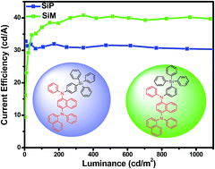
Yellow electrophosphorescent devices with hosts containing N1-(naphthalen-1-yl)-N1,N4-diphenylnaphthalene-1,4-diamine and tetraphenylsilane units

Song Zhang, Qiu-Lei Xu, Yi-Ming Jing, Xuan Liu, Guang-Zhao Lu, Xiao Liang, You-Xuan Zheng* and Jing-Lin Zuo
State Key Laboratory of Coordination Chemistry, Collaborative Innovation Center of Advanced Microstructures, School of Chemistry and Chemical Engineering, Nanjing University, Nanjing 210093, P. R. China. E-mail: yxzheng@nju.edu.cn

Received 9th February 2015 , Accepted 11th March 2015

First published on 11th March 2015


Abstract

Two novel host materials, N1-(naphthalen-1-yl)-N1,N4-diphenyl-N4-(4-(triphenylsilyl)phenyl) naphthalene-1,4-diamine (SiP) and N1-(naphthalen-1-yl)-N1,N4-diphenyl-N4-(3-(triphenylsilyl) phenyl)naphthalene-1,4-diamine (SiM), were synthesised by incorporating a hole-transporting moiety, N1-(naphthalen-1-yl)-N1,N4-diphenylnaphthalene-1,4-diamine (NPNA2) and typical electron-transporting tetraphenylsilane moiety. SiP and SiM materials exhibit high thermal and morphological stability with a glass transition temperature higher than 110 °C and decomposition temperature above 350 °C. Using Ir(bt)2(acac) (bis(2-phenylbenzothiozolato-N,C2′)iridium(acetylacetonate)) as an emitter, yellow phosphorescent organic light-emitting diodes of ITO/TAPC (1,1-bis[4-(di-p-tolylamino)phenyl]cyclohexane, 40 nm)/host: Ir(bt)2(acac) (15 wt%, 20 nm)/TmPyPB (1,3,5-tri(m-pyrid-3-yl-phenyl)benzene, 40 nm)/LiF (1 nm)/Al (100 nm) show maximum current and power efficiency of 40.81 cd A−1 and 33.60 lm W−1 with low efficiency roll-off. The current efficiency of 40.10 cd A−1 is still observed at the practically useful brightness value of 1000 cd m−2.

Introduction

Organic light-emitting diodes (OLEDs) have been available on the market for over a decade and it is now a multi-billion dollar industry-mostly from touch-enabled active-matrix OLED (AMOLED) displays for mobile phones. In 1998, phosphorescent OLEDs (PHOLEDs) were first reported by Ma and Forrest et al.1 In contrast to typical fluorescent OLEDs, PHOLEDs have attracted considerable attention because they can reach 100% of the theoretical internal quantum efficiency by harvesting both singlet and triplet excitons.1,2 In PHOLEDs, to reduce the quenching associated with the relatively long exciton lifetimes, long diffusion lengths of triplet emitters and triplet–triplet annihilation, phosphorescent emitters of heavy-metal complexes are usually doped into a suitable host material.3 It is desirable that the host materials ought to have a large enough triplet energy gap for efficient energy transfer to the guest, good carrier transport properties for a balanced recombination of holes and electrons in the emitting layer, energy-level matching with neighboring layers for effective charge injection4 and high thermal and morphological stability. Among many design concepts for host materials, bipolar host materials have been the subject of interest because these materials have well-balanced charge transport properties that could extend the recombination zone, improve the device efficiency and simplify the device structure.5 The incorporation of hole-transporting (donor) and electron-transporting (acceptor) moieties into the multifunctional host materials has been proved to be an efficient method to obtain bipolar small molecules. However, the conjugation caused by intramolecular donor–acceptor interactions may lower the triplet energies of bipolar molecules. Therefore, the development of the bipolar host possessing high triplet energy is still interesting for practical application. One of strategies adopted to suppress the donor–acceptor interactions for confining the triplet energy on the emitting phosphors is to introduce a π-conjugated bridge with a twisted conformation, which can partially reduce the electronic coupling of the donor and acceptor in the ground state. More efficiently, the incorporation of saturated centers such as sp3-C or Si as the molecular bridge can usually block the electronic interactions between the hole-transporting and electron-transporting substructures.4 Silicon atoms are used in host materials due to many advantages, such as conjugation blocking for a wide band gap and a tetrahedral geometry for morphology.6

The dimer of the N-phenyl-1-naphthylamine, N1-(naphthalen-1-yl)-N1,N4-diphenylnaphthalene-1,4-diamine (NPNA2, ET = 2.67 eV, low temperature photoluminescence spectra shown in Fig. S1), has ever been characterized to have high triplet energy, excellent hole-transporting ability and high thermal stability. Our previous research also demonstrated the successful utilization of the dimer of N-phenyl-1-naphthylamine as an effective electron-donating moieties in hole-transporting layer.7 In the case of that, we adopted the hole-transporting moiety to two new silicon-based host materials, N1-(naphthalen-1-yl)-N1,N4-diphenyl-N4-(4-(triphenylsilyl)phenyl) naphthalene-1,4-diamine (SiP) and N1-(naphthalen-1-yl)-N1,N4-diphenyl-N4-(3-(triphenylsilyl)phenyl)naphthalene-1,4-diamine (SiM) by introducing triphenylsilane to the para- and meta-positions of a phenyl linker (Scheme 1). The triplet energy of the two host materials was almost the same because it is determined by the novel hole-transporting moiety NPNA2, which is higher than a widely used yellow phosphor of Ir(bt)2(acac) (bis(2-phenylbenzothiozolato-N,C2′)iridium(acetylacetonate)),8 and efficient energy transfer from the host materials to the Ir(bt)2(acac) is expected.


image file: c5ra02475g-s1.tif
Scheme 1 Synthetic routes of SiP and SiM.

Results and discussion

Synthesis and thermal property

Scheme 1 shows the synthetic routes and structures of SiP and SiM. 1,4-Dibromobenzene and 1,3-dibromobenzene were sequentially treated with n-butyl-lithium and chlorotriphenylsilane to obtain (4-bromophenyl)triphenylsilane and (3-bromophenyl)triphenylsilane, respectively. Buchwald–Hartwig crossing-coupling of both organic halides with N1-(naphthalen-1-yl)-N1,N4-diphenylnaphthalene-1,4-diamine (NPNA2) gave SiP and SiM with yields higher than 65%.

The thermal property of host material is very important for stable OLEDs. The thermal gravimetric analysis (TGA) and differential scanning calorimetry (DSC) curves of SiP and SiM under a nitrogen atmosphere were listed in Fig. 1. Both compounds exhibit good thermal stabilities and the decomposition temperatures (Td), which correspond to a 5% weight loss upon heating during TGA, were measured as 397 and 351 °C for SiP and SiM, respectively. And their corresponding glass transition temperatures (Tg) are 134 and 116 °C, respectively. The Tg values of the new compounds are much higher than those of the most reported bipolar hosts, such as the analogous silane-modified UGHs which had undesired low glass transition temperature in the range of 26–53 °C.9 The high Tg values of these host materials may be mainly attributed to the configuration of the dimer of the N-phenylnaphthalen-1-amine, which can suppress intermolecular aggregation and improve the film morphology. The high Td and Tg values of SiP and SiM are expected to decrease the phase separation rate of the guest–host system upon heating and have the potential use in high performance devices fabricated by vacuum thermal evaporation technology.10


image file: c5ra02475g-f1.tif
Fig. 1 TG curves of SiP (black line) and SiM (red line). Inset: DSC curves of SiP (black line) and SiM (red line).

Photophysical and electrochemical property

The absorption spectra of SiP, SiM and Ir(bt)2(acac) were tested in dichloromethane solution (Fig. 2). The absorption at 268 nm is attributed to the NPNA2-centered n–π* transition. The longer wavelength absorption observed at 378 nm for SiP and 381 nm for SiM are attributed to the π–π* transitions from the electron-donating NPNA2 moiety to the electron-accepting tetraphenylsilane moiety. The absorption bands of (bt)2Ir(acac) at 441 and 481 nm are belong to the absorption transition from ground state to singlet 1MLCT and triplet 3MLCT excited state.11 The photoluminescence spectra of SiP, SiM host materials and Ir(bt)2(acac) at room temperature or 77 K are also shown in Fig. 2. The maximum emission peak of Ir(bt)2(acac) located at 560 nm with a slight shoulder at 597 nm. The emission peaks of SiP and SiM at room temperature are 452 and 451 nm, respectively, suggesting the position of triphenylsilane on phenyl linker has negligible effect on the emission. There is a good overlap between the fluorescence bands of two novel hosts and the MLCT absorption of Ir(bt)2(acac), suggesting a possible energy transfer from SiP and SiM to Ir(bt)2(acac). The triplet energies of the SiP and SiM were determined as 2.64 and 2.67 e V, respectively, from the highest energy vibronic sub-band of their phosphorescence spectra at 77 K (Table 1). From their triplet alignments, it also can be speculated that there should be an efficient energy transfer from host triplet states to the Ir(bt)2(acac) triplet states and an excellent triplet energy confinement on the Ir(bt)2(acac) molecules within the emissive layers.
image file: c5ra02475g-f2.tif
Fig. 2 UV-vis spectra of SiP, SiM and Ir(bt)2(acac) in dichloromethane solution at room temperature; photoluminescence spectra in dichloromethane solution at 298 K of SiP, SiM and Ir(bt)2(acac); phosphorescence spectra in dichloromethane solution glass matrix of SiP and SiM at 77 K.
Table 1 Photophysical data of compounds SiP and SiM
Compound Td/Tga (°C) Absorptionb λ (nm) Emission λemb (nm) 298 K ETc (eV) HOMO (eV) LUMO (eV)
a Tg: glass transition temperatures, Td: decomposition temperatures.b Measured in dichloromethane solution at room temperature.c Triplet energy: estimated from the highest-energy peaks of the 77 K phosphorescence spectra.
SiP 397/134 268/378 452 2.64 −5.19 −2.31
SiM 351/116 268/381 451 2.67 −5.18 −2.27


The redox properties and highest occupied molecular orbital (HOMO), lowest unoccupied molecular orbital (LUMO) energy levels of the hosts are relative to the charge transport ability and the OLED structure. For evaluation the HOMO/LUMO energy levels, the electrochemical properties of SiP and SiM were probed by cyclic voltammetry (CV) using ferrocene as the internal standard (Fig. S2). The hosts exhibited two reversible oxidation and reduction behaviors, which were most likely resulting from the electrochemical properties of the NPNA2 moiety. The oxidation potentials of SiP and SiM were found at 0.392 and 0.382 V versus Ag/Ag+, respectively. According to the equation EHOMO = −(Eonsetox + 4.8) eV,12 the HOMO levels of SiP and SiM were estimated to be approximately −5.19 and −5.18 eV, respectively, which is about 0.31 and 0.32 eV higher than that of TAPC (5.50 eV),13 and thus theoretically barrier-free hole injection from the hole-transport layer can be realized.14 The corresponding LUMO levels calculated from the HOMO values and the band gaps (2.88 and 2.91 eV) were found to be approximately −2.31 and −2.27 eV, respectively.

OLEDs performance

To compare the charge-transporting properties of SiP and SiM, the current density–voltage (JV) characteristics of hole-only devices (HOD) with the configuration ITO/host (30 nm)/TAPC (1,1-bis[4-(di-p-tolylamino)phenyl]cyclohexane, 60 nm)/Al (100 nm) and electron-only devices (EOD) with the configuration ITO/TmPyPB (1,3,5-tri(m-pyrid-3-yl-phenyl)benzene, 60 nm)/host (60 nm)/LiF (1 nm)/Al (100 nm) were investigated. The TAPC or TmPyPB layer was used to prevent electron- or hole-injection from cathode or anode, respectively. In general, asymmetric substitution at the meta-position would be an effective strategy for the design of high-performance bipolar host materials.15 However, HODs and EODs showed two hosts were not found obvious bipolar characters because the hole current density is two orders of magnitude higher than the electron current density (Fig. 3). These results demonstrate that the hole transport properties of NPNA2-based electron-donating moiety is much better than the electron transport properties of tetraphenylsilane-based electron-withdrawing moiety. Furthermore, SiP and SiM exhibit negligible differences of electron mobility (Fig. 3(b)). But the hole transport ability of SiP is little higher than that of SiM at same driving voltages. Considering the similar physical properties of two compounds, the slightly different carrier-transporting properties between SiP and SiM are probably due to their different steric configurations.
image file: c5ra02475g-f3.tif
Fig. 3 Current density–voltage of hole-only (a) and electron-only (b) devices made of SiP and SiM.

Using the traditional multilayer device configuration ITO/TAPC (40 nm)/host: Ir(bt)2(acac) (15 wt%, 20 nm)/TmPyPB (40 nm)/LiF (1 nm)/Al (100 nm), we investigated the function of SiP and SiM as hosts. The molecule structures and energy level diagrams of the materials and devices are shown in Fig. 4. TAPC and TmPyPB were used as the hole- and electron-transporting layers, respectively. Ir(bt)2(acac) was used as the phosphor emitter with the optimized doping concentration of 15 wt%, which is a little higher than common yellow devices.16 This may be attributed to the LUMO level of Ir(bt)2(acac) (−2.95 eV) which was significantly lower than that of two hosts, electrons had the potential to be trapped at Ir(bt)2(acac). At higher doping level, more electrons were injected directly to the dopant molecules, which provided an additional channel to transport electrons through hopping between the dopant sites.17 Accordingly, higher dopant concentration such as 15 wt% improved the charge balance and energy transfer from host to guest. Though the HOMO level of Ir(bt)2(acac) (−5.29 eV) is lower than that of SiP and SiM, there is near no energy barrier for the hole transport from TAPC to dopant and hosts due to the higher HOMO level of TAPC (Fig. 4).


image file: c5ra02475g-f4.tif
Fig. 4 Energy level diagram of yellow PHOLEDs and molecular structures of materials used.

The electroluminescence (EL) spectra of the devices are listed in Fig. 5; the current density–voltage–luminance (JVL), current efficiency–luminance (ηcL) and power efficiency–luminance (ηpL) curves are shown in Fig. 6. The key device performance parameters are summarized in Table 2. The EL spectra of the SiP- and SiM-based yellow PHOLEDs showed a main peak at 563 or 565 nm and a slight shoulder peak appeared at 595 nm from Ir(bt)2(acac). There is no peak origin from SiP and the emission from SiM are very weak. This suggests that the emission peaks are indeed derived from the dopant, and the triplet energy transfer from the hosts to the dopant are nearly complete. The Commission Internationale de l'Eclairage (CIE) color coordinates of the SiP- and SiM-based devices are (0.49, 0.48) and (0.51, 0.47), respectively.


image file: c5ra02475g-f5.tif
Fig. 5 Electroluminescence spectra measured at 8.0 V.

image file: c5ra02475g-f6.tif
Fig. 6 (a) Current density–voltage–luminance (JVL); (b) current efficiency–luminance (ηcL) and power efficiency–luminance (ηpL) characteristics of the PHOLEDs with SiP and SiM.
Table 2 Electroluminescence performances of the devices based on SiP and SiM
Host Vturn-ona (V) Lmax (voltage)b [cd m−2 (V)] ηc,max (luminance)c [cd A−1 (cd m−2)] ηc,L1000d (cd A−1) ηp,maxe [lm W−1] EQEmaxf (%) CIEg (x,y)
a Vturn-on: turn-on voltage recorded at a luminance of 1 cd m−2.b Lmax: maximum luminance.c ηc,max: maximum current efficiency.d ηc,L1000: current efficiency at 1000 cd m−2.e ηp,max: maximum power efficiency.f EQEmax: maximum external quantum efficiency.g Measured at 8 V.
SiP 2.9 36[thin space (1/6-em)]731 (10.0) 31.96(172.09) 30.30 30.79 11.10 0.49,0.48
SiM 2.9 37[thin space (1/6-em)]768 (10.2) 40.81(343.01) 40.10 33.60 15.10 0.51,0.47


Both SiP- and SiM-based devices have low turn-on voltages of 2.9 V at a luminance of 1 cd m−2. The main reason for such low turn-on voltage is the relative high HOMO energy levels of the two hosts and there is no barrier against a hole transport from TAPC into SiP or SiM. The low LUMO of Ir(bt)2(acac) and 15 wt% doped concentration also lowered the energy loss for the electron transport from TmPyPB to the emissive layer. As anticipated from the charge-transporting ability results, the device using SiP as host show higher current density than SiM-based device (Fig. 6(a)). From Fig. 6(b) it can be observed that the SiM-based device has a maximum current efficiency of 40.81 cd A−1 and a maximum external quantum efficiency (EQE) of 15.1% at a luminance of 343.01 cd m−2 with mild efficiency roll-off. At the practical luminance of 1000 cd m−2, the current efficiency of 40.10 cd A−1 can be obtained. Even at the luminance of 10[thin space (1/6-em)]000 cd m−2, a current efficiency around 32 cd A−1 still can be maintained. As a result of the low driving voltage, the SiM device also shows maximum power efficiency of 33.60 lm W−1.

On the other hand, the efficiencies of SiP-based device (a maximum current efficiency ηc,max of 31.96 cd A−1, a maximum external quantum efficiency EQE of 11.10% and a maximum power efficiency ηp,max of 30.79 lm W−1) were slightly lower than that of the SiM-based device. This result can be understood by considering the hole- and electron-transport properties of two hosts. It should be noted that the hole mobility of TAPC (hole mobility (μh) ≈ 10−2 cm2 V−1 s−1)18 is higher than the electron mobility of TmPyPB (electron mobility (μe) ≈ 10−3 cm2 V−1 s−1)19 and in this case, the hole-trapping recombination mechanism may affects the efficiencies of the devices. More imbalance of holes and electrons injection will cause more serious hole-trapping in the emitting layer. At the low current density, hole-trapping could provide an additional emission process and will improve the efficiency.20 However, the more trapped holes will lead to triplet-polaron quenching and induce the efficiency roll-off when the current density increased.21 Therefore, the relative low hole mobility and more balanced carriers in the SiM-based device could lead to a relatively higher utilization ratio of the carriers in the emissive layer, resulting in the higher efficiency.

Conclusions

In conclusion, two novel host materials SiP and SiM have been synthesized by attaching the N1-(naphthalen-1-yl)-N1,N4-diphenylnaphthalene-1,4-diamine moiety to the triphenylsilane segment via the para- and meta-position of the N-phenyl. Both compounds exhibit good thermal stabilities with glass transition temperatures of 134 and 116 °C, respectively. The host materials have sufficient triplet energy (ET > 2.6 eV) for good energy transfer to yellow phosphor Ir(bt)2(acac). In traditional multilayer structures, a device with SiP as a host achieved maximum ηc,max/ηp,max of 31.96 cd A−1/30.79 lm W−1 and SiM-based device achieved maximum ηc,max/ηp,max of 40.81 cd A−1/33.60 lm W−1. This study indicates that the new hole-transporting moiety is an excellent unit for building host materials for efficient yellow PHOLEDs.

Experimental

Materials and measurements

1H NMR and 13C NMR spectra were measured on a Bruker AM 500 spectrometer and a Bruker AM 126 spectrometer, respectively. Mass spectra (MS) were obtained with MALDI-TOF (Bruker Daltonic Inc.). High resolution mass spectra (Agilent 6540 UHD Accurate-Mass Q-TOF LC/MS) were recorded for the compounds. TGA and DSC measurements were carried out on STA 449F3 (NETZSCH) and 823e (METTLER), respectively. Absorption and emission spectra were measured on a Shimadzu UV-3100 and a Hitachi F-4600 luminescence spectrophotometer, respectively. The low temperature phosphorescence spectra were measured with an Edinburgh Instruments FLS-920 spectrophotometer at 77 K. Cyclic Volta metric experiments were carried out with an CHI 600E system (Chenhua, Shanghai) using three electrode cell assemblies in deaerated dichloromethane solution with tetrabutylammoniumperchlorate as supporting electrolyte at a scan rate of 100 mV s−1. Each oxidation potential was calibrated with ferrocene as a reference.

OLEDs fabrication and measurement

Organic chemicals used for OLEDs were generally purified by high-vacuum, gradient temperature sublimation. The devices were fabricated by vacuum deposition of the materials at 10−6 Torr onto a ITO (indium tin oxide) glass substrate (a sheet resistance of 15 Ω per square) with a deposition rate of 1–2 Å s−1. The phosphor and host were co-evaporated to form 20 nm emitting layer from two separate sources. The LiF and Al were deposited with deposition rates of 0.1 and 3 Å s−1, respectively. The characteristics of the devices were measured with a computer controlled KEITHLEY 2400 source meter with a calibrated silicon diode in air without device encapsulation. The CIE coordinates were calculated using a testing program of the Spectra scan PR650 spectrophotometer.

Syntheses

All reactions were performed under nitrogen. Solvents were carefully dried and distilled from appropriate drying agents prior to use for syntheses of ligands. NPNA2 was synthesised according to our previous report.7
4-Bromophenyltriphenylsilane. 12.5 mL of a 1.6 M solution of n-BuLi (20 mmol) in hexane is added dropwise to a solution of 4.72 g, 3.027 mL (20 mmol) of 1,4-dibromobenzene in 100 mL of ether at −78 °C. Then the mixture is allowed to warm up to ambient temperature within 2.5 h. The mixture is again cooled to −78 °C and 5.90 g of chlorotriphenylsilane (20 mmol, resolved in ether) is added in a dropwise manner. After warming the mixture to ambient temperature and stirring overnight the solvent is removed in vacuo and the residue was purified by column chromatography on silica gel using n-hexane as the eluent to give a white powder. Yield: 75%. MS (MALDI-TOF, m/z) calcd for C24H19SiBr: 414.044. Found: 413.949 [M]+.
3-Bromophenyltriphenylsilane. 3-Bromophenyltriphenylsilane was prepared according to the same procedure as compound 4-bromophenyltriphenylsilane but 1,3-dibromobenzene instead of 1,4-dibromobenzene was used as a starting material. Yield: 72%. MS (MALDI-TOF, m/z) calcd for C24H19SiBrNa+: 439.031. Found: 440.450 [M + Na]+.
N1-(Naphthalen-1-yl)-N1,N4-diphenyl-N4-(4-(triphenylsilyl) phenyl)naphthalene-1,4-diamine (SiP). Pd2(dba)3 (0.09 g, 0.10 mmol), NPNA2 (0.04 g, 1.0 mmol), LitBuO (0.32 g, 4.0 mmol), and (4-bromophenyl)triphenylsilane (0.50 g, 1.2 mmol) were added into a 50 mL two-neck flask. The flask was evacuated and backfilled with nitrogen. o-Xylene (20 mL) and PtBu3 (1.23 mL, 0.4 mmol, 10% in n-hexane) were injected. The mixture was heated at 140 °C for 48 h and extracted twice with CH2Cl2 at room temperature. The mixed organic solution was washed with brine and dried over anhydrous sodium sulfate. The solid obtained was purified with column chromatography on SiO2 using ethyl acetate and petroleum ether (v[thin space (1/6-em)]:[thin space (1/6-em)]v = 1[thin space (1/6-em)]:[thin space (1/6-em)]50) as eluant to afford 0.51 g SiP (0.67 mmol, 67%). 1H NMR (500 MHz, CDCl3, Fig. S3) δ[ppm] 8.12 (d, J = 8.4 Hz, 1H), 8.08 (d, J = 8.5 Hz, 1H), 8.02 (d, J = 8.3 Hz, 1H), 7.91 (d, J = 8.2 Hz, 1H), 7.73 (d, J = 8.2 Hz, 1H), 7.60–7.54 (m, 6H), 7.51–7.47 (m, 1H), 7.42 (dd, J = 7.5, 3.8 Hz, 3H), 7.40–7.34 (m, 11H), 7.27–7.22 (m, 5H), 7.17 (dd, J = 15.6, 7.6 Hz, 5H), 6.99 (d, J = 8.4 Hz, 3H), 6.89 (d, J = 7.3 Hz, 1H), 6.77 (d, J = 7.6 Hz, 2H). 13C NMR (126 MHz, CDCl3, Fig. S5) δ[ppm] 150.44, 149.65, 147.57, 144.70, 143.51, 140.33, 137.32, 136.42, 135.28, 134.75, 132.89, 131.68, 130.30, 129.50, 129.25, 129.05, 128.55, 127.84, 126.66, 126.51, 126.34, 126.21, 126.11, 125.85, 125.38, 125.15, 125.12, 124.84, 124.78, 124.44, 123.01, 122.63, 120.78, 120.40, 119.54. HR EI-MS (m/z) calcd for C56H42N2Si: 770.3117. Found: 770.3115 [M]+ (Fig. S7). IR (KBr, cm−1, Fig. S9): 3131.80, 1585.93, 1492.32, 1458.88, 1394.12, 1282.60, 1108.21, 768.86, 700.51, 517.02.
N1-(Naphthalen-2-yl)-N1,N4-diphenyl-N4-(3-(triphenylsilyl) phenyl)naphthalene-1,4-diamine (SiM). Compound SiM was prepared according to the same procedure as compound SiP but (3-bromophenyl)triphenylsilane instead of (4-bromophenyl)triphenylsilane was used as a starting material. Yield: 65%. 1H NMR (500 MHz, CDCl3, Fig. S4) δ[ppm] 8.13–8.08 (m, 1H), 8.06 (d, J = 8.5 Hz, 1H), 8.02–7.96 (m, 1H), 7.91 (d, J = 8.2 Hz, 1H), 7.72 (d, J = 8.1 Hz, 1H), 7.48–7.46 (m, 6H), 7.39–7.35 (m, 5H), 7.34 (dd, J = 5.7, 3.9 Hz, 3H), 7.31 (s, 2H), 7.25–7.21 (m, 3H), 7.20 (d, J = 4.4 Hz, 3H), 7.17 (d, J = 7.3 Hz, 3H), 7.10 (dd, J = 12.6, 7.3 Hz, 4H), 7.04 (d, J = 7.9 Hz, 3H), 6.90 (dd, J = 17.0, 7.5 Hz, 3H), 6.71 (d, J = 7.9 Hz, 2H). 13C NMR (126 MHz, CDCl3, Fig. S6) δ[ppm] 150.43, 148.29, 147.69, 144.70, 143.14, 140.79, 136.28, 135.27, 135.05, 134.15, 132.64, 131.70, 130.25, 129.74, 129.70, 129.53, 129.06, 129.01, 128.81, 128.52, 127.82, 127.52, 126.47, 126.41, 126.28, 126.21, 126.08, 125.75, 125.35, 125.07, 124.96, 124.44, 123.19, 121.53, 121.45, 120.66, 120.34. HR EI-MS (m/z) calcd for C56H42N2Si: 770.3117. Found: 770.3122 [M]+. (Fig. S8) IR (KBr, cm−1): 3132.19, 3063.67, 1584.75, 1487.75, 1459.44, 1392.49, 1282.24, 1108.03, 769.60, 744.19, 701.22, 510.40 (Fig. S10).

Acknowledgements

This work was supported by the National Natural Science Foundation of China (21371093, 91433113), the Major State Basic Research Development Program (2011CB808704, 2013CB922101) and the Natural Science Foundation of Jiangsu Province (BK20130054).

References

  1. (a) Y. G. Ma, H. Y. Zhang, J. C. Shen and C. M. Che, Synth. Met., 1998, 94, 245 CrossRef CAS; (b) M. A. Baldo, D. F. O'Brien, Y. You, A. Shoustikov, S. Sibley, M. E. Thompson and S. R. Forrest, Nature, 1998, 395, 151 CrossRef CAS PubMed.
  2. (a) P.-T. Chou and Y. Chi, Chem.–Eur. J., 2007, 13, 380 CrossRef CAS PubMed; (b) Y. Chi and P.-T. Chou, Chem. Soc. Rev., 2010, 39, 638 RSC; (c) L. Xiao, Z. Chen, B. Qu, J. Luo, S. Kong, Q. Gong and J. Kido, Adv. Mater., 2011, 23, 926 CrossRef CAS PubMed; (d) C.-H. Fan, P. Sun, T.-H. Su and C.-H. Cheng, Adv. Mater., 2011, 23, 2981 CrossRef CAS PubMed; (e) H.-H. Chou, Y.-K. Li, Y.-H. Chen, C.-C. Chang, C.-Y. Liao and C.-H. Cheng, ACS Appl. Mater. Interfaces, 2013, 5, 6168 CrossRef CAS PubMed; (f) X. Xu, X. Yang, J. Dang, G. Zhou, Y. Wu, H. Li and W.-Y. Wong, Chem. Commun., 2014, 50, 2473 RSC; (g) X. Yang, G. Zhou and W.-Y. Wong, J. Mater. Chem. C, 2014, 2, 1760 RSC.
  3. W. Jiang, L. Duan, J. Qiao, G. Dong, D. Zhang, L. Wang and Y. Qiu, Dyes Pigm., 2012, 92, 891 CrossRef CAS PubMed.
  4. (a) A. Chaskar, H.-F. Chen and K. T. Wong, Adv. Mater., 2011, 23, 3876 CrossRef CAS PubMed; (b) S.-H. Chou, W.-Y. Hung, C.-M. Chen, Q.-Y. Liu, Y.-H. Liu and K.-T. Wong, RSC Adv., 2013, 3, 13891 RSC.
  5. (a) K. S. Yook and J. Y. Lee, Adv. Mater., 2012, 24, 3169 CrossRef CAS PubMed; (b) L. Duan, J. Qiao, Y. Sun and Y. Qiu, Adv. Mater., 2011, 23, 1137 CrossRef CAS PubMed.
  6. (a) W.-S. Han, H.-J. Son, K.-R. Wee, K.-T. Min, S. Kwon, I.-H. Suh, S.-H. Choi, D.-H. Jung and S.-O. Kang, J. Phys. Chem. C, 2009, 113, 19686 CrossRef CAS; (b) R. J. Holmes, B. W. D'Andrade, S. R. Forrest, X. Ren, J. Li and M. E. Thompson, Appl. Phys. Lett., 2003, 83, 3818 CrossRef CAS PubMed; (c) X. M. Liu, C. B. He, J. C. Huang and J. M. Xu, Chem. Mater., 2005, 17, 434 CrossRef CAS; (d) X.-M. Liu, C. B. He, X.-T. Hao, L.-W. Tan, Y. Q. Li and K. S. Ong, Macromolecules, 2004, 37, 5965 CrossRef CAS; (e) X. M. Liu, J. W. Xu, X. H. Lu and C. B. He, Org. Lett., 2005, 7, 2829 CrossRef CAS PubMed; (f) D.-R. Bai and S. N. Wang, Organometallics, 2004, 23, 5958 CrossRef CAS; (g) H.-C. Yeh, C.-H. Chien, P.-I. Shih, M.-C. Yuan and C.-F. Shu, Macromolecules, 2008, 41, 3801 CrossRef CAS; (h) S.-J. Yeh, M.-F. Wu, C.-T. Chen, Y.-H. Song, Y. Chi, M.-H. Ho, S.-F. Hsu and C. H. Chen, Adv. Mater., 2005, 17, 285 CrossRef CAS; (i) M.-F. Wu, S.-J. Yeh, C.-T. Chen, H. Murayama, T. Tsuboi, W.-S. Li, I. Chao, S.-W. Liu and J.-K. Wang, Adv. Funct. Mater., 2007, 17, 1887 CrossRef CAS; (j) M.-H. Tsai, H.-W. Lin, H.-C. Su, T.-H. Ke, C.-C. Wu, F.-C. Fang, Y.-L. Liao, K.-T. Wong and C.-I. Wu, Adv. Mater., 2006, 18, 1216 CrossRef CAS; (k) J.-J. Lin, W.-S. Liao, H.-J. Huang, F.-I. Wu and C.-H. Cheng, Adv. Funct. Mater., 2008, 18, 485 CrossRef CAS.
  7. S. Zhang, L.-S. Xue, Y.-M. Jing, X. Liu, G.-Z. Lu, X. Liang, H.-Y. Li, Y.-X. Zheng and J.-L. Zuo, Dyes Pigm., 2015 DOI:10.1016/j.dyepig.2015.02.011.
  8. C. Fan, L. P. Zhu, B. Jiang, Y.-F. Li, F.-C. Zhao, D.-G. Ma, J.-G. Qin and C.-L. Yang, J. Phys. Chem. C, 2013, 117, 19134 CAS.
  9. (a) P.-I. Shih, C.-H. Chien, C.-Y. Chuang, C.-F. Shu, C.-H. Yang, J.-H. Chen and Y. Chi, J. Mater. Chem., 2007, 17, 1692 RSC; (b) X. F. Ren, J. Li, R. J. Holmes, P. I. Djurovich, S. R. Forrest and M. E. Thompson, Chem. Mater., 2004, 16, 4743 CrossRef CAS; (c) S.-L. Gong, Q. Fu, Q. Wang, C.-L. Yang, C. Zhong, J.-G. Qin and D.-G. Ma, Adv. Mater., 2011, 23, 4956 CrossRef CAS PubMed.
  10. C.-J. Zheng, J. Ye, M.-F. Lo, M.-K. Fung, X.-M. Ou, X.-H. Zhang and C.-S. Lee, Chem. Mater., 2012, 24, 643 CrossRef CAS.
  11. (a) X. Wei, J. Peng, J. Cheng, M. Xie, Z. Lu, C. Li and Y. Cao, Adv. Funct. Mater., 2007, 17, 3319 CrossRef CAS; (b) S. M. Chen, G. P. Tan, W.-Y. Wong and H.-S. Kwok, Adv. Funct. Mater., 2011, 21, 3785 CrossRef CAS.
  12. (a) Q. Sun, H. Wang, C. Yang and Y. Li, J. Mater. Chem., 2003, 13, 800 RSC; (b) J. Pommerehne, H. Vestweber, W. Guss, R. F. Mahrt, H. Bassler, M. Porsch and J. Daub, Adv. Mater., 1995, 7, 551 CrossRef CAS.
  13. G. Liaptsis and K. Meerholz, Adv. Funct. Mater., 2013, 23, 359 CrossRef CAS.
  14. B. H. Zhang, G. P. Tan, C.-S. Lam, B. Yao, C.-L. Ho, L. H. Liu, Z. Y. Xie, W.-Y. Wong, J. Q. Ding and L. X. Wang, Adv. Mater., 2012, 24, 1873 CrossRef CAS PubMed.
  15. M.-K. Yan, Y. Tao, R.-F. Chen, C. Zheng, Z.-F. An and W. Huang, RSC Adv., 2012, 2, 7860 RSC.
  16. H.-F. Chen, T.-C. Wang, S.-W. Lin, W.-Y. Hung, H.-C. Dai, H.-C. Chiu, K.-T. Wong, M.-H. Ho, T.-Y. Cho, C.-W. Chen and C.-C. Lee, J. Mater. Chem., 2012, 22, 15620 RSC.
  17. F.-M. Hsu, C.-H. Chien, P.-I. Shih and C.-F. Shu, Chem. Mater., 2009, 21, 1017 CrossRef CAS.
  18. Y. Miao, X. Du, H. Wang, H. Liu, H. Jia, B. Xu, Y. Hao, X. Liu, W. Li and W. Huang, RSC Adv., 2014, 5, 4261 RSC.
  19. S.-J. Su, T. Chiba, T. Takeda and J. Kido, Adv. Mater., 2008, 20, 2125 CrossRef CAS.
  20. (a) C. Han, F. Zhao, Z. Zhang, L. Zhu, H. Xu, J. Li, D. Ma and P. Yan, Chem. Mater., 2013, 25, 4966 CrossRef CAS; (b) F. Zhao, N. Sun, H. Zhang, J. Chen and D. J. Ma, Appl. Phys., 2012, 112, 084504 CrossRef PubMed; (c) Q. Wang, J. Ding, D. Ma, Y. Cheng, L. Wang, X. Jing and F. Wang, Adv. Funct. Mater., 2009, 19, 84 CrossRef CAS.
  21. J. Jin, W. Zhang, B. Wang, G. Mu, P. Xu, L. Wang, H. Huang, J. Chen and D. Ma, Chem. Mater., 2014, 26, 2388 CrossRef CAS.

Footnote

Electronic supplementary information (ESI) available: For the photoluminescence spectra of NPNA2 in dichloromethane solution at 298 and 20 K, cyclic voltammograms of SiP and SiM in dichloromethane solution. See DOI: 10.1039/c5ra02475g

This journal is © The Royal Society of Chemistry 2015
Click here to see how this site uses Cookies. View our privacy policy here.