
A micro/nano-multiscale hierarchical structure strategy to fabricate highly conducting films for electromagnetic interference shielding and energy storage†
Beibei
Wang
ad,
Weiye
Zhang
ad,
Jingmeng
Sun
ad,
Chenhuan
Lai
b,
Shengbo
Ge
b,
Hongwu
Guo
*ad,
Yi
Liu
 *ad and
Daihui
Zhang
*bc
*ad and
Daihui
Zhang
*bc
aKey Laboratory of Wood Material Science and Application (Beijing Forestry University), Ministry of Education, Beijing 100083, China. E-mail: guohongwu_305@bjfu.edu.cn; liuyichina@bjfu.edu.cn
bCo-Innovation Center of Efficient Processing and Utilization of Forest Resources, Nanjing Forestry University, Nanjing 210037, Jiangsu, China. E-mail: Daihui.zhang@mail.mcgill.ca
cInstitute of Chemical Industry of Forest Products, Chinese Academy of Forestry, Nanjing, Jiangsu 210042, China
dEngineering Research Center of Forestry Biomass Materials and Energy, Ministry of Education, Beijing Forestry University, Beijing 100083, China
First published on 8th March 2023
Abstract
Ultrathin, strong, flexible, and conductive materials have garnered considerable attention in foldable wearable electronics and electromagnetic interference (EMI) shielding. However, their preparation remains challenging to simultaneously achieve desired high-performance electrochemical and EMI properties. Herein, we describe a micro/nano-multiscale hierarchical structure strategy to fabricate TEMPO-oxidized cellulose nanofibrils (TOCNFs)/Ti3C2Tx MXene/silver nanowire (AgNW) hybrid films via a facile alternating vacuum-filtration process, followed by hot-pressing. The micro/nanoscale design enabled the films to exhibit excellent EMI and electrochemical properties simultaneously. Specifically, the FM2Ag2 (TOCNFs/Ti3C2Tx/AgNW = 1![[thin space (1/6-em)]](https://www.rsc.org/images/entities/char_2009.gif) :2:2) hybrid film exhibited outstanding mechanical properties with a tensile strength of 85.63 ± 7.24 MPa, excellent electrical conductivity of 1.29 × 10⁷ S m−1, superior EMI shielding effectiveness (EMI SE) of 45.57 dB, and high SSE/t of 26014.52 dB cm2 g−1. Moreover, it maintained a high areal and specific capacitance of 110.7 mF cm−2 and 77.6 F g−1 at 10 mV s−1, respectively, accompanied by impressive stability with 92.4% capacitance retention after 10000 cycles. This study proposes a novel and facile micro/nano-multiscale hierarchical structure strategy to effectively balance the electrochemical and EMI properties. This paves the way for the fabrication of robust multifunctional films for potential applications in precise instruments and next-generation electronics.
:2:2) hybrid film exhibited outstanding mechanical properties with a tensile strength of 85.63 ± 7.24 MPa, excellent electrical conductivity of 1.29 × 10⁷ S m−1, superior EMI shielding effectiveness (EMI SE) of 45.57 dB, and high SSE/t of 26014.52 dB cm2 g−1. Moreover, it maintained a high areal and specific capacitance of 110.7 mF cm−2 and 77.6 F g−1 at 10 mV s−1, respectively, accompanied by impressive stability with 92.4% capacitance retention after 10000 cycles. This study proposes a novel and facile micro/nano-multiscale hierarchical structure strategy to effectively balance the electrochemical and EMI properties. This paves the way for the fabrication of robust multifunctional films for potential applications in precise instruments and next-generation electronics.
1 Introduction
Energy storage devices have developed rapidly owing to the recent popularity of wearable electronics.1–3 Nevertheless, traditional metal electrodes used in supercapacitors have several disadvantages, including severe corrosion, lack of flexibility, and high potential toxicity to the environment. The prosperity of electronic telecommunication technology has promoted the wide utilization of electronic devices and caused serious concerns owing to the inevitable electromagnetic radiation pollution.4 Although highly conductive metal-based materials have been widely utilized, their low flexibility, high density, poor chemical resistance, and processability limit their applications. Similar technological challenges have been presented for electrodes and electromagnetic interference (EMI) materials.3,5,6 Therefore, it is of interest to fabricate new ultrathin, strong, flexible, and conductive materials that simultaneously show impressive electrochemical activity while possessing great EMI shielding. This will not only improve the application range of the materials, but also avoid producing electromagnetic pollution from electronic devices, and failure caused by outside electromagnetic interference. Unfortunately, few approaches are successful in fabricating such conductive materials for both applications at the same time. Thus, it is necessary to develop an efficient strategy to obtain conductive materials that exhibit the above-mentioned properties.As a unique family of two-dimensional (2D) transition metal materials, MXenes exhibit chemically active surfaces, hydrophilicity, and high conductivity. They have been extensively explored in the fields of energy storage and EMI shielding.1,7–9 For example, Yu et al. have demonstrated transparent MXene–silver nanowire films through a sequential dispersion and evaporation process for EMI shielding applications.10 Jin et al. have proposed a crack-template-assisted spraying methodology for fabricating flexible, transparent, and conductive MXene grid–silver nanowire hierarchical films for EMI shielding.11 Tian et al. have successfully fabricated freestanding and mechanically robust MXene and cellulose nanofibril (CNF) nanocomposites for supercapacitors.12 However, van der Waals forces and hydrogen bonds are present during the assembly process, which can cause serious re-stacking of MXene nanosheets. This can damage their performance as energy storage and EMI shielding materials, owing to the reduction in electromagnetic reflection loss, reabsorption capacity, and ion-accessible surface areas.13,14 Additionally, they can further increase the density of materials, thereby affecting their advantages as lightweight materials. Therefore, the elimination of MXene aggregation to effectively assemble them into highly conductive three-dimensional (3D) structures has been a significant challenge.
Several approaches, including a direct coating on porous structures and construction of vertically aligned MXene structures or hydrogels, have been proposed to effectively resolve the MXene re-stacking issues.15–18 Specifically, the addition of other nanocomponents to tune the MXene assembly process during vacuum-assisted filtration has proven its simplicity, effectiveness, and scalability.19,20 Particularly, one-dimensional (1D) CNFs have garnered considerable attention in the fabrication of MXene-based films owing to their renewability and hydrophilicity, and ability to offer enhanced mechanical properties.3,5,21 Liu et al. have demonstrated an efficient strategy for reinforcing electrically conductive MXene films with GO sheets by bridging the MXene sheets with hydrogen bonds, which maintained superb mechanical properties (209 MPa), a high electrical conductivity (4.62 × 10⁴ to 2.64 × 10⁵ S m−1), and an EMI SE of over 50 dB.22 Wang et al. have fabricated an ultrathin carbon nanotube/cellulose nanofiber/Ti3C2Tx film for EMI shielding and energy storage. The obtained films exhibited a high specific SSE/t of 9316.4 dB cm2 g−1, and an areal and specific capacitance of 537 mF cm−2 and 279.7 F g−1 at 0.3 mA cm−2, respectively.23 Despite the development, the incorporation of CNFs inevitably leads to relatively poor conductivity because of their insulation properties. The comprehensive performance of MXene films as both EMI shielding and electrode materials has been compromised.5,24
Biomimetic designs have been widely adopted to prepare unique materials.25–28 Jia et al. have developed flexible conducting electrodes with an ultralow sheet resistance by mimicking vein-like conductive networks on the molecular scale.29 Nevertheless, very poor mechanical properties were observed due to the lack of enhancement fillers. Fortunately, recent studies have highlighted the significance of microscale structural engineering strategies to enhance the mechanical properties without significantly affecting conductivity.30,31 For example, asymmetric sandwich structured cellulose-based MXene films have been prepared for EMI shielding. The utilization of cellulose layers to cover the conductive layer provided a strong tensile strength of 118.0 MPa, accompanied by high conductivity (37378.2 S m−1) and outstanding specific SSE/t (10647.6 dB cm2 g−1).32 However, insulated cellulose layers as the surface may potentially influence its electrochemical performance. In addition, a double-layered structure composed of aramid nanofibers and MXene/silver nanowires has been fabricated. Despite its high strength (235.9 MPa), the SSE/t was only 10688.9 dB cm2 g−1 with a thickness of over 30 μm.33 This could be also due to the insulating nature of one layer. Liu et al. have demonstrated a vacuum-assisted layer-by-layer assembly technique to conformally deposit leaf-like electrically conductive substances on textiles for developing multifunctional and flexible textiles with superb EMI shielding performances (54 dB).34 Therefore, inspired by the previous work, we hypothesize that the combination of nanoscale-designed leaf-like conductive layers and microscale-assembled sandwich structures (TOCNFs in the middle as an enhanced layer) can fabricate strong, ultrathin, flexible, and highly conductive MXene-based materials, simultaneously achieving high EMI shielding and improved energy storage performance.33
Herein, a micro/nano-multiscale hierarchical structure strategy was presented to prepare ultrathin, strong, flexible, and highly conductive TOCNFs/Ti3C2Tx/AgNW hybrid films via a facile alternating vacuum-filtration process, followed by hot pressing (Scheme 1). Micro/nano-scale integrated regulation was the key to the design. On the nanoscale, the leaf-like biomimetic top and bottom conductive layers offered high conductivity to the films, while the microscale structural engineering of sandwich structures provided excellent mechanical properties, flexibility, and enhanced functionalities. This micro/nano-scale design was significantly different from previous studies, where all the components were generally mixed together.35,57 Therefore, the obtained films simultaneously showed excellent EMI shielding and electrochemical properties. This study proposes a novel and facile micro/nano-multiscale hierarchical structure strategy for effectively fabricating high-performance films in the field of precise instrument, smart electronics and flexible/wearable devices.
 | ||
| Scheme 1 Schematic illustration for a multiscale strategy to fabricate TOCNFs/Ti3C2Tx/AgNW hybrid films. | ||
2 Experimental
2.1 Materials
Sodium hydroxide (NaOH, 99%), sodium bromide (NaBr, 99%), TEMPO, and sodium hypochlorite (NaClO, 99%) were purchased from Sigma Aldrich Co. LLC. Layered ternary carbide (Ti3AlC2, MAX) powder was supplied by Jilin 11 Technology Co. Ltd. Ag nanowires (5 mg mL−1) were supplied by Zhengzhou Feynman Biotechnology Co. Ltd. All chemicals were of analytical grade.2.2 Synthesis of TEMPO-oxidized cellulose nanofibrils (TOCNFs)
TOCNFs were synthesized following a previously reported method.23,36,37 Typically, TEMPO (0.016 g, 0.1 mM) and NaBr (0.1 g, 1 mM) were placed into a softwood pulp suspension (100 mL, 1 wt%) in a glass beaker. NaClO solution (5 mmol g−1) was used to initiate the reaction. NaOH solution (0.5 M) was used to maintain a pH of 10.5 during the oxidation process. After 5 h of reaction, 10 mL of ethanol was used to stop the reaction, and HCl was used to adjust the pH to 7.0. After thorough washing, the TOCNFs were redispersed in deionized (DI) water. Subsequently, the upper dispersion was collected via centrifugation. The evenly dispersed TOCNFs (1.0 wt%) were obtained by using a high-pressure homogenizer.2.3 Preparation of Ti3C2Tx MXene nanosheets
Ti3C2Tx MXene was synthesized by etching the Ti3AlC2 MAX phase using a wet chemical etching method.38–40 Briefly, LiF (1.6 g) was dissolved in 9 M HCl solution (20 mL) by stirring. The Ti3AlC2 powder (1.0 g) was added slowly to the solution and stirred at 45 °C for 1 d. Further, they were washed and centrifuged repeatedly until the Ti3C2Tx supernatant turned dark green. Sonication in an ice bath was used to treat the exfoliated Ti3C2Tx solution. Finally, the solution was centrifuged to collect the supernatant with a concentration of 5 mg mL−1.2.4 Preparation of TOCNFs/Ti3C2Tx/AgNW hybrid films with a sandwich structure
TOCNFs/Ti3C2Tx/AgNW hybrid films were prepared using an alternating vacuum-assisted filtration method (Scheme 1). Ti3C2Tx/AgNW (20 mg) was evenly divided into bottom (10 mg) and top (10 mg) parts, while the middle layer consisted of TOCNFs (5 mg). TOCNFs/Ti3C2Tx/AgNW hybrid films with a sandwich structure were easily fabricated via a three-step vacuum-assisted filtration. Firstly, the uniform Ti3C2Tx/AgNW aqueous mixture obtained by sonication and stirring (20 mL) with a concentration of 0.5 mg mL−1 was vacuum filtered onto a filter membrane until a stable Ti3C2Tx/AgNW hydrogel was yielded. Subsequently, the TOCNF dispersion (10 mL, 0.5 mg mL−1) was deposited on the top of the Ti3C2Tx/AgNW hydrogel. Finally, the Ti3C2Tx/AgNW aqueous mixture (20 mL, 0.5 mg mL−1) was deposited on the top of the TOCNF hydrogel in the same way. The total mass of each film was maintained at ∼25 mg, and the diameter is 40 mm. The weight ratios of F (TOCNFs), M (Ti3C2Tx), and Ag (AgNW) were selected based on F/M = 1:4, F/M/Ag = 1:3:1, F/M/Ag = 1:2:2, F/M/Ag = 1:1:3, and F/Ag = 1:4. For instance, FM3Ag indicates that the total mass of Ti3C2Tx was 15 mg and that of AgNWs was 5 mg. Thus, each side of the layer contained 7.5 mg of Ti3C2Tx and 2.5 mg of AgNWs, and the middle layer contained 5 mg of TOCNFs. The hybrid films were then dried at 65 °C and 1 MPa in a vacuum oven, followed by peeling off to obtain freestanding TOCNFs/Ti3C2Tx/AgNW hybrid films. For comparison, a homogeneously mixed TOCNFs/Ti3C2Tx/AgNW hybrid film (mass ratio = 1:2:2), labeled FM2Ag2-mix, was prepared via one-step vacuum-assisted filtration.
2.5 Characterization
X-ray diffraction (XRD, SmartLab, Rigaku Ultima IV) was conducted using Cu-Kα radiation (40 kV and 44 mA) in the 2-theta range of 3–63° with a scan speed of 5° min−1. Atomic force microscopy (AFM) was performed in the tapping mode (Agilent 5500). Field-emission scanning electron microscopy (FE-SEM, JSM-6700F, JEOL) and high-resolution transmission electron microscopy (HR-TEM, JEM-2100F, JEOL) were used to investigate the morphologies and microstructures. A Fourier-transform infrared spectrometer (FTIR, Thermo Scientific Nicolet iS5) was used to record the spectra of the films in the range 400–4000 cm−1. Surface chemistry was examined using X-ray photoelectron spectroscopy (XPS, ESCALAB 250 Xi, Thermo Fisher). Nitrogen sorption was performed at −196 °C using a Quadrasorb instrument (Quantachrome NOVE 2000e, USA). A microcomputer-controlled electron universal testing machine (100 N load cell) was used to conduct the mechanical tests. According to GB/T457-2008 Paper and Board-Determination of Folding Endurance, the folding resistance of the samples was tested under a 4.9 N load at a 135° ± 2° folding angle by using a folding tester (PN-NZ135, China). The strips were 9.5 × 25 mm2 and the rate was 0.5 mm min−1 (C42.503Y). Contact angles were recorded using a commercial instrument (POWER EACH JC2000C1) to determine the initial contact angles. The electrical conductivities of the hybrid films were measured using an RTS-9 four-probe resistivity meter (4ProbesTech, Guangzhou, China), and different parts of the film were measured at least three times to obtain an average. The electrical conductivity was obtained using eqn (1): | (1) |
If multiple reflections were negligible for a total shielding efficiency of larger than 15 dB, the SEtotal can be written as follows (Simon's formula):
 | (2) |
The EMI SE of the hybrid films was measured within 8.2–12.4 GHz (X-band) using a Keysight N5224BPNA network analyzer (E5071C, Agilent). The sample was supported with an epoxy resin frame (22.9 × 10.2 mm2, 0.5 mm in width) as the separator. When electromagnetic radiation interacts with a material during the test (shield), the shielding phenomenon is governed by absorption (A), reflection (R), and transmission (T):42
| R + A + T = 1 | (3) |
The transmission (T) and reflection (R) coefficients can be obtained from the network analyzer (S11, S12, S21, and S22):
| R = |S11|2 = |S22|2 | (4) |
| T = |S12|2 = |S21|2 | (5) |
The total EMI shielding value (EMI SEtotal) is the total contribution from multiple internal reflections (SEM), reflection (SER), and absorption (SEA). The SEtotal can be written as follows:
| SEtotal = SEA + SER + SEM | (6) |
For calculations, the SEM is generally considered negligible when SEtotal is higher than 15 dB.43–45 The SER and SEA can be derived in terms of the reflection and absorption coefficients as follows:
 | (7) |
 | (8) |
When the density and thickness of materials are considered, relevant equations are as follows:
 | (9) |
 | (10) |
The EMI shielding efficiency (%) can be calculated by using eqn (11):
 | (11) |
The light-to-heat conversion performance was evaluated using an MC-PF300C solar simulator under simulated solar light. An infrared thermal imager (Beijing Merry Change Technology Co. Ltd.) was used to monitor the temperature variation.
The electrochemical performance of the film electrodes was measured using an electrochemical workstation (CHI760E, China). Three-electrode electrochemical tests were performed in 1 M H2SO4 electrolyte, and the reference and counter electrodes were Ag/AgCl and platinum sheets, respectively. TOCNFs/Ti3C2Tx/AgNW hybrid films were punched into a size of 1 × 2 cm2 and were directly used as the working electrodes with no binders. Electrochemical impedance spectroscopy (EIS) tests were performed in a frequency range of 100 kHz to 0.01 Hz. Cyclic voltammetry (CV) at various scan rates and galvanostatic charge–discharge (GCD) at various current densities were both achieved at a potential of −0.2 to 0.3 V. The specific capacitance in the three-electrode system was obtained from CV curves,46 as follows:
 | (12) |
For the impedance spectra, the real (C′) and imaginary (C′′) parts of the capacitances are as follows:47
 | (13) |
 | (14) |
Kinetic characterization of the film electrode was performed to elucidate the electrochemical energy storage mechanism. To explore the energy-storage process of the membrane electrode, CV curves at different scan rates were analyzed by using the formulae as follows:
| i = is + id = avb | (15) |
| Logi = blogv + loga | (16) |
Formula (15) can be converted into the following form:
| i(V) = k1v + k2v1/2 | (17) |
3 Results and discussion
3.1 Characterization of TOCNFs, Ti3C2Tx MXene, and AgNW nanomaterials
TEMPO can selectively oxidize the hydroxyl group at the C6 position of the glucose molecule to a carboxyl group,48 forming TOCNF nanostructures. Thus, the electrostatic repulsion between fiber surfaces accounts for the excellent dispersion of TOCNFs in an aqueous solution (Fig. S1a†).48,49 TEM and AFM reveal that TOCNFs were approximately 5–20 nm in diameter and 100–500 nm in length (Fig. S1b and c†). The dense pure TOCNF film obtained after vacuum filtration is shown in Fig. S1d, e and S2† illustrates the preparation of the 2D MXene nanosheets using the typical fluorine-containing acidic solution method. The Al layer was selectively etched with HCl/LiF on the stacked Ti3AlC2 structure (Fig. S3†) to obtain multilayer Ti3C2Tx (m-Ti3C2Tx). Subsequently, with ultrasonic delamination, m-Ti3C2Tx can be exfoliated into single- or few-layer Ti3C2Tx nanosheets (MXene). These nanosheets formed stable colloidal solutions (Fig. S4a†) because of the hydrophilic groups on the terminal surface, such as –OH, –F, and![[double bond, length as m-dash]](https://www.rsc.org/images/entities/char_e001.gif) O, and no sedimentation and flocculation were observed at 6 °C for over 30 d. Furthermore, the as-prepared Ti3C2Tx nanosheets were irregular with an ultrathin thickness of approximately 1.5 nm and an average size of approximately 2 μm (Fig. S4b–g†) with smooth surfaces without oxide particles. The corresponding selected area electron diffraction (SAED) pattern exhibited a well-defined hexagonal structure (Fig. S4f†), indicating no defects. After vacuum filtration, the cross-sectional SEM images confirmed that 2D Ti3C2Tx nanosheets were easily assembled into ultrathin pure MXene films (Fig. S5†). In addition, as shown in the XRD patterns of the Ti3AlC2 precursor and as-exfoliated Ti3C2Tx (Fig. S6†), there was an obvious left shift of the (002) peak from 9.5° to 7.3° caused by the increased interlayer spacing. Furthermore, the characteristic peaks corresponding to (101), (103), (104), and (105) almost disappeared.51 Pristine Ti3C2Tx showed clear diffraction peaks for the MXene basal planes. The surface chemical compositions of Ti3AlC2 and Ti3C2Tx were determined using XPS (Fig. S7 and S8†). It shows the successful etching of Al in the presence of Ti–O (2p3) and Ti–C (2p3) doublets for monolayer Ti3C2Tx nanosheets, which is consistent with previous reports.40,52–54 For the AgNWs, the average diameter was ∼40 nm with an average length of ∼10 μm (Fig. S9†). All the obtained TOCNFs, Ti3C2Tx, and AgNW dispersions displayed a strong Tyndall effect, demonstrating their good colloidal characteristics.
O, and no sedimentation and flocculation were observed at 6 °C for over 30 d. Furthermore, the as-prepared Ti3C2Tx nanosheets were irregular with an ultrathin thickness of approximately 1.5 nm and an average size of approximately 2 μm (Fig. S4b–g†) with smooth surfaces without oxide particles. The corresponding selected area electron diffraction (SAED) pattern exhibited a well-defined hexagonal structure (Fig. S4f†), indicating no defects. After vacuum filtration, the cross-sectional SEM images confirmed that 2D Ti3C2Tx nanosheets were easily assembled into ultrathin pure MXene films (Fig. S5†). In addition, as shown in the XRD patterns of the Ti3AlC2 precursor and as-exfoliated Ti3C2Tx (Fig. S6†), there was an obvious left shift of the (002) peak from 9.5° to 7.3° caused by the increased interlayer spacing. Furthermore, the characteristic peaks corresponding to (101), (103), (104), and (105) almost disappeared.51 Pristine Ti3C2Tx showed clear diffraction peaks for the MXene basal planes. The surface chemical compositions of Ti3AlC2 and Ti3C2Tx were determined using XPS (Fig. S7 and S8†). It shows the successful etching of Al in the presence of Ti–O (2p3) and Ti–C (2p3) doublets for monolayer Ti3C2Tx nanosheets, which is consistent with previous reports.40,52–54 For the AgNWs, the average diameter was ∼40 nm with an average length of ∼10 μm (Fig. S9†). All the obtained TOCNFs, Ti3C2Tx, and AgNW dispersions displayed a strong Tyndall effect, demonstrating their good colloidal characteristics.
3.2 Multiscale design and morphologies of TOCNFs/Ti3C2Tx/AgNW hybrid films
A schematic of the multiscale fabrication of the AgNW-intercalated Ti3C2Tx MXene hybrid films with TOCNFs as a reinforcing agent is shown in Scheme 1. Ultrathin sandwich-structured hybrid films were prepared via continuous stratified filtration of Ti3C2Tx/AgNW and TOCNF aqueous solutions, followed by hot pressing and drying treatment. Directly mixing all components into a solution was also utilized to prepare a film (FM2Ag2-mix) for comparison. The variation in the components significantly influenced the appearance of the films, as shown in Fig. 1a. Furthermore, Fig. 1d–i depicts the SEM images of the 45° inclined plane view of the TOCNFs/Ti3C2Tx/AgNW and FM2Ag2-mix hybrid films. Three-layer structures with electrically conductive MXene/AgNW on the top and bottom layers and mechanically strong TOCNFs in the middle were observed for the TOCNFs/Ti3C2Tx/AgNW films (Fig. 1b), as compared to the relatively homogeneous structure of FM2Ag2-mix. Furthermore, the unique structure was further studied by SEM-EDS mapping measurements owing to the different element distributions (Fig. 1c).55 The top and bottom Ti3C2Tx/AgNW layers exhibited leaf-like nanostructures. 1D AgNWs served as conductive frameworks (veins) and could prevent the stacking of Ti3C2Tx, whereas 2D Ti3C2Tx behaved as a connection (lamina) (Fig. 1f).33 The efficient nanoscale design and integration of Ti3C2Tx and AgNWs built a continuous 3D conductive network on both sides, which is beneficial for the construction of the conductive pathway.56 In comparison, the FM2Ag2-mix film exhibited a “brick-mortar” structure with a relatively uniform distribution of TOCNFs, Ti3C2Tx, and AgNWs10,57 (Fig. 1i).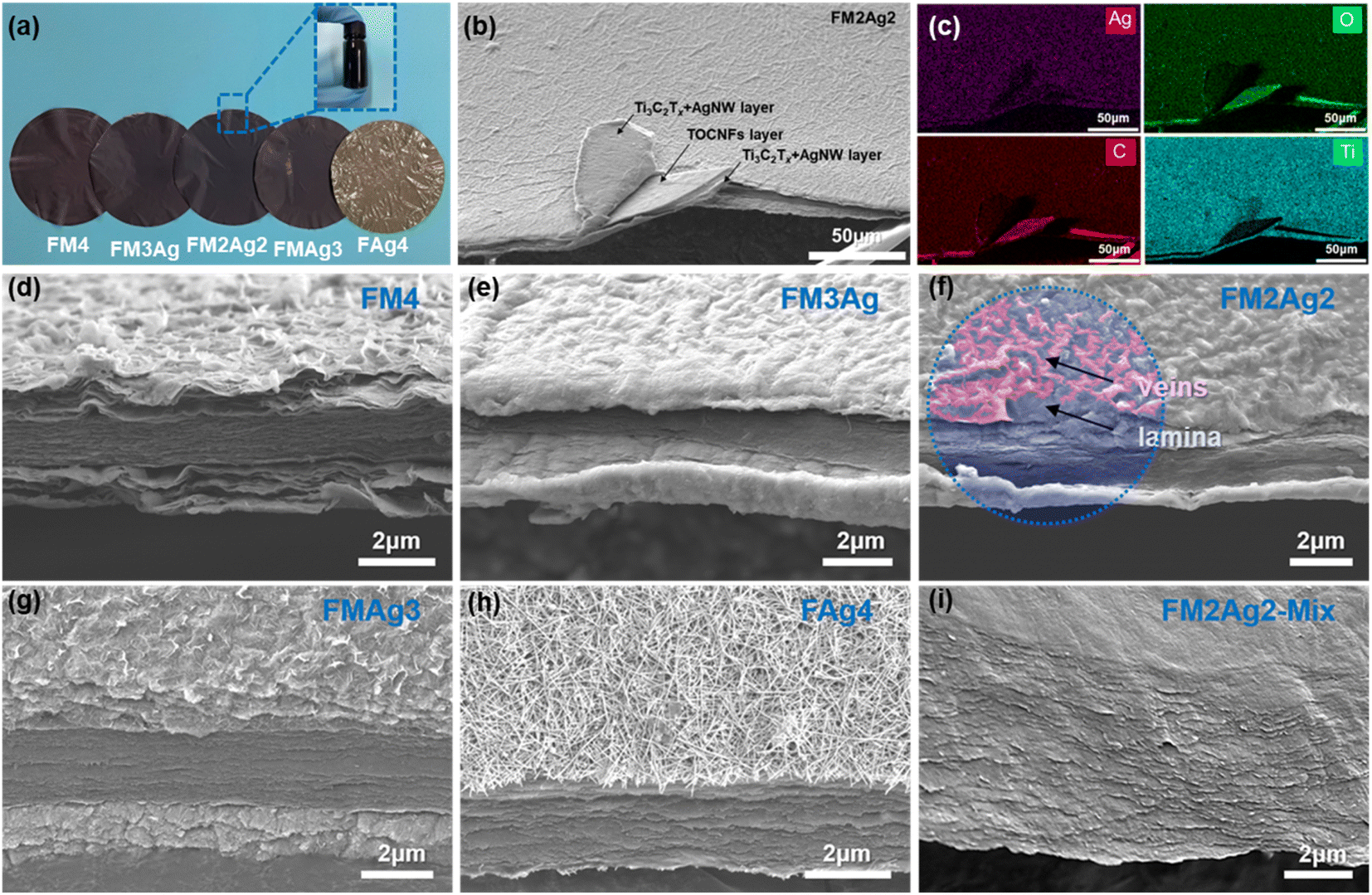 | ||
| Fig. 1 (a) Digital photo of the TOCNFs/Ti3C2Tx/AgNW hybrid films and mixed solutions of FM2Ag2. (b) FE-SEM image. (c) EDS mapping images of FM2Ag2; 45° inclined plane view of (d) FM4, (e) FM3Ag, (f) FM2Ag2, (g) FMAg3, (h) FAg4, and (i) FM2Ag2-mix. | ||
3.3 Physicochemical properties of the TOCNFs/Ti3C2Tx/AgNW hybrid films
The physicochemical properties of the TOCNFs/Ti3C2Tx/AgNW hybrid film were analyzed by FTIR, XRD, and XPS (Fig. 2a–d and S10–S14†). Specifically, FM2Ag2-mix showed a strong broad peak at 3474 cm−1, corresponding to the O–H stretching vibration, and the asymmetric and symmetric vibrations of –COOH were observed at 1635 cm−1 and 1466 cm−1, respectively. For the FM2Ag2 hybrid film, the intensity of the –OH stretching vibration peak decreased significantly and shifted from 3474 to 3383 cm−1, indicating the formation of hydrogen bonds (Fig. 2a).58–60 For sandwich-structured films, Ti3C2Tx acted as a binder to reduce the damage of the mechanical strength caused by the separation of adjacent AgNWs. Moreover, the formation of hydrogen bonds could effectively prevent the exfoliation of AgNWs, thereby improving the durability of hybrid films. The phase structures of TOCNFs/Ti3C2Tx/AgNW hybrid films are shown in Fig. 2b and S11.† The characteristic (002) peak at 7.3° for Ti3C2Tx gradually shifted to 6.1° for FM2Ag2, indicating a relatively uniform interstitial space between interlayers.50 The d002 interlayer spacing was 1.45 nm by calculation. Additionally, for FM2Ag2-mix, the (002) diffraction peak further shifted to a lower angle of 5.6° with d002 = 1.58 nm. This comparison reveals that TOCNFs could be partially inserted between Ti3C2Tx and AgNWs to increase the interlayer space. Furthermore, the hybrid film exhibited distinct diffraction peaks located at 38.2° and 44.7°, corresponding to the (111) and (200) crystalline planes of AgNWs, respectively.20,61Fig. 2c, d and S12–S14† present the XPS wide-scan spectra of the TOCNFs/Ti3C2Tx/AgNW hybrid film and high-resolution spectra of C 1s, Ag 3d, Ti 2p, F 1s, and O 1s. The AgNW-doped TOCNFs/Ti3C2Tx/AgNW hybrid films showed an additional characteristic peak of the Ag 3d mode from AgNWs (Fig. S13a†). Its intensity in FM3Ag, FM2Ag2, FMAg3, and FM2Ag2-mix was very weak because of the low AgNW content, except for FAg4. The characteristic Ti 2p and F 1s bonding modes of Ti3C2Tx-containing films were similar (Fig. S13b and c†). However, for C 1s and O 1s, the binding energies varied significantly (Fig. 2d and S13d†).61 For example, the peaks of C–O (287.0 eV) and CO (288.9 eV) shifted to higher binding energies in FM2Ag2-mix (287.5 and 289.7 eV, respectively). This result is consistent with those of previous studies.61 For example, the peaks of C–O at 287.0 eV and CO at 288.9 eV shifted to higher binding energies in FM2Ag2-mix (287.5 and 289.7 eV, respectively). This result is consistent with those of previous studies, indicating the formation of hydrogen bonds within the films.23,58
 | ||
| Fig. 2 (a) FT-IR, (b) XRD patterns, (c) XPS survey scan spectra, (d) C 1s spectra, (e) N2 adsorption–desorption isotherms, and (f) pore size distribution based on the DFT model of FM2Ag2 and FM2Ag2-mix. (g) Tensile stress–strain curves. (h) Calculated mechanical properties, and (i) toughness and Young's modulus of TOCNFs/Ti3C2Tx/AgNW hybrid films. | ||
The exposed surface area and pore distribution of the FM2Ag2 and FM2Ag2-mix hybrid films were further investigated by N2 adsorption/desorption measurements (Fig. 2e and f). The adsorption–desorption isotherm curves show a type-IV behavior with distinct H3 hysteresis loops. This result reveals the generation of uniform mesopores with a high specific surface area and large total pore volume. The specific surface area of the FM2Ag2 hybrid film was 17.9 m2 g−1, as calculated by Brunauer–Emmett–Teller (BET) analysis, which was larger than that of FM2Ag2-mix (13.8 m2 g−1). The reduced specific surface area indicates that TOCNFs enabled the FM2Ag2-mix film to be tighter because of the enhanced interactions. This may lead to a decrease in the electromagnetic shielding performance and electrochemical properties. Furthermore, the pore size distribution in FM2Ag2 and FM2Ag2-mix hybrid films was mainly centered at 4.15 nm, which originated from the channel pores derived from the AgNW support between Ti3C2Tx nanosheets35 (Fig. 1f). The pore volumes of these two films were 0.086 cm3 g−1 and 0.063 cm3 g−1, respectively.
The mechanical test showed that films with a sandwich structure (50.5–116.1 MPa) had better mechanical properties than the homogeneously mixed film (40.95 ± 5.29 MPa) (Fig. 2g and S15†). Without doping of Ti3C2Tx or AgNWs, a dense reinforcement layer in the middle was formed due to the stronger hydrogen bonds between TOCNFs, which thus significantly improve the mechanical properties of films (Fig. S1d†). Furthermore, the composition of the top and bottom layers can also significantly influence the mechanical properties. Owing to the better mechanical properties of Ti3C2Tx,18,62 an increase in its proportion leads to an enhancement in the tensile strength, toughness, and modulus. In addition, hydrogen bonds, electrostatic interaction, and van der Waals interactions between Ti3C2Tx/AgNW and TOCNFs help improve tensile strength. For example, FM2Ag2 showed a tensile strength, toughness, and modulus of 85.63 ± 7.24 MPa, 1.02 ± 0.10 MJ m−3, and 5.18 ± 0.29 GPa, respectively, as compared to 49.48 ± 5.67 MPa, 0.33 ± 0.07 MJ m−3, and 4.55 ± 0.67 GPa of FAg4 (Fig. 2h, i and Table S1†). Besides, the tensile strength of the pure TOCNF film (25 mg) determined by a tensile test could reach 104.09 ± 5.18 MPa,23 while pure Ti3C2Tx and pure AgNW films were too brittle to effectively test. Moreover, we tested the folding resistance of the hybrid films, as shown in Fig. S16.† FM4 and FM3Ag could be folded more than 3000 times. FM2Ag2 can be folded approximately 2400 times. However, the foldability performance of FM2Ag2-mix was significantly reduced, and only approximately 750 times were obtained. The folding number of the hybrid films was approximately 5–23 times greater than that of commercial A4 paper (∼140 times). The flexibility and stability of the obtained sandwich-structured films were significantly improved because of the condensed interlayer generated by the strong hydrogen bonds in TOCNFs. Moreover, all the hybrid films displayed good flexibility owing to the introduction of TOCNFs (Fig. S17a and b†). For the FM2Ag2 hybrid film, no cracks or fractures were observed by applying a 500 g weight, showing its excellent flexibility (Fig. S17c†).
3.4 EMI shielding performance of the TOCNFs/Ti3C2Tx/AgNW hybrid films
The shielding performance of incident electromagnetic waves was evaluated by using the EMI SE.1,63 The mechanically strong and ultrathin sandwich-structured TOCNFs/Ti3C2Tx/AgNW hybrid films exhibited a low surface resistance with an increase in AgNWs (Fig. 3a), which was significantly higher than the requirement (1 S m−1) in practical applications.64 The electrical conductivities of FM4 and FAg4 were the lowest (1.05 × 10⁶ S m−1) and highest (2.77 × 10⁷ S m−1), respectively. This indicates that AgNWs can enhance the electrical conductivity of the hybrid films. Crucially, one-dimensional AgNWs were tangled together to form a continuous percolated network, which constructed hierarchical structures for increasing electron transport channels with high conductivity.11,20 The conductivity of FM2Ag2 reached approximately 1.29 × 10⁷ S m−1, which was much higher than that of homogeneously mixed FM2Ag2-mix (3.98 × 10⁵ S m−1). This is attributed to the highly efficient Ti3C2Tx/AgNW conducting network in the layered structure,33 which is not affected by insulated TOCNFs.23 Notably, the well-designed sandwich-structured films exhibited conductive anisotropy with improved conductivity along the in-plane direction and insulating properties along the cross-plane direction. The change in conductivity was further examined by visual inspection of the brightness of light-emitting diodes (LEDs) (Fig. 3a). In addition, attaching FM2Ag2 to finger joints showed no significant increase in resistance after 100 bending cycles (Fig. 3b), proving its good flexibility and stable electrical conductivity. Fig. 3c and S18† show the EMI shielding performance of TOCNFs/Ti3C2Tx/AgNW hybrid films with stable fluctuation ranging from 8.2–12.4 GHz (X-band). Compared with FM2Ag2-mix, the sandwich-structured films exhibited much higher EMI shielding ability. In particular, the FM2Ag2 film (4 μm in thickness) presented a high EMI SE of 51.30 dB (higher than the commercial requirement of 20 dB), whereas it was only 24.67 dB for FM2Ag2-mix (3 μm in thickness) (Fig. S19†), which was ascribed to the direct mixing of TOCNFs, resulting in the condensation phenomenon. Additionally, the EMI SE of FAg4 increased to a maximum of 73.55 dB (5 μm in thickness), following the trend of conductivity. The total EMI shielding effectiveness (SEtotal), microwave absorption (SEA), and microwave reflection (SER) over the X-band were calculated by using formulas (6)–(8) (Fig. 3c and S18†). The SEA predominantly contributed to the overall shielding performance of the films; however, the SER value barely increased (Fig. 3c and d). With an increase in the number of FM2Ag2 layers (layers of Ti3C2Tx/AgNW (10 mg:10 mg) and TOCNF (5 mg)), the SEtotal and SEA of the films exhibited a significant enhancement, whereas the SER remained unchanged. The increase in the SEA contribution by multiple reflections dominated the improvement in the overall shielding (Fig. 3d).10 The porous structure offered more interfaces for the electromagnetic waves to be reflected and scattered efficiently.65 The AgNW-doped sandwich-structured films possessed higher EMI shielding efficiencies and could obtain a shielding efficiency of more than 99.99%, for example, 99.9993% for FM2Ag2, whereas the homogeneously mixed FM2Ag2-mix hybrid film could only block 99.65% (Fig. S20†).
 | ||
| Fig. 3 (a) Electrical conductivity and LED brightness for the TOCNFs/Ti3C2Tx/AgNW hybrid films. (b) Electrical resistance variation of FM2Ag2 with the bending test. (c) SEtotal, SEA, and SER. (d) EMI shielding performances of stacked structures with different layers. (e) Schematic illustration of the electromagnetic wave transfer across the TOCNFs/Ti3C2Tx/AgNW hybrid films. (f) SSE/t values with different thicknesses. (g) Comparison of specific electrical conductivity, EMI shielding effectiveness, and thickness with others, and the references are listed in Table S2;† (h) performance comparison of FM2Ag2 and FM2Ag2-mix, and (i) infrared images of temperature variation for FM2Ag2 after exposure to solar light. | ||
To demonstrate the potential mechanism, the transfer process of electromagnetic waves across the sandwich-structure hybrid films is illustrated in Fig. 3e. As the electromagnetic waves impinge on the surfaces of hybrid films, some waves are immediately reflected due to the impedance mismatch caused by the abundant free electrons on the surface.33,66 These repeated reflections and scattering effectively enhanced the transmission of the electromagnetic wave energy.66–68 Additionally, the remaining polar groups (–OH, –F, etc.) of Ti3C2Tx also triggered the asymmetric distribution of generated local dipoles in the electric field and charge density, resulting in polarization relaxation and thus enhancing EMI shielding performance.66,69 Meanwhile, the microcurrent can interact with high-density electron carriers to induce a large ohmic loss and attenuation of electromagnetic wave energy by currents, leading to the absorption of electromagnetic waves. EMI shielding was enhanced by the layer-structured design at the same total loading of Ti3C2Tx/AgNW.10 The passing electromagnetic waves could then be reflected and absorbed by the bottom conductive layer. In addition, as the EMI shielding performance is positively correlated with the thickness and electrical conductivity,7,39,41,70 the SSE/t (SE divided by sample density and thickness) was then calculated (Fig. 3f). The SSE/t of sandwich-structured films increased from 13918.31 to 40165.72 dB cm2 g−1 at 8.2 GHz, superior to most of the previously reported Ti3C2Tx and silver-based hybrid films (Fig. 3g and Table S2†). Moreover, FM2Ag2 (28016.19 dB cm2 g−1) also had two times higher electromagnetic shielding effectiveness than FM2Ag2-mix (13474.13 dB cm2 g−1). Thus, the sandwich-structured films showed a better performance than the homogeneously mixed film, owing to their enhanced conductivity, high pore volumes, surface areas, and multiple-layer structures (Fig. 3h).
As shown in Fig. 3i, the photothermal conversion performance of FM2Ag2 was measured under simulated solar light (one sun intensity). After irradiation for 80 s, the temperature rapidly jumped to 59.6 °C, gradually increased to 67.5 °C after 160 s, and gradually stabilized at 83.9 °C after 240 s. The excellent photothermal conversion performance of composite films was mainly attributed to the local surface plasmon resonance (LSPR) effect and strong light absorption of Ti3C2Tx/AgNW.71 Moreover, this indicates that absorption, particularly additive internal absorption, leads to a loss of energy in electromagnetic waves. The absorbed EM waves are mainly dissipated in the form of heat energy generated by effective electron migration, which is consistent with the enhancement in electrical conductivity.72,73 This result proves the high electromagnetic wave absorption capacity of this material, which has potential in photothermal conversion.
3.5 Electrochemical performance of the TOCNFs/Ti3C2Tx/AgNW hybrid films
The electrochemical performance of the TOCNFs/Ti3C2Tx/AgNW hybrid film electrodes for electrochemical energy storage was evaluated using galvanostatic charge–discharge (GCD), cyclic voltammetry (CV), electrochemical impedance spectroscopy (EIS), and cycling stability in a 3-electrode electrochemical cell using 1 M H2SO4 in a potential window of −0.2 to 0.3 V (vs. Ag/AgCl). CV was performed to assess the charge–discharge storage mechanism of the TOCNFs/Ti3C2Tx/AgNW electrode (Fig. 4a, b and S21a–e†). A voltage window of 0.5 V was used to avoid the oxidation of the material.74,75 It was reported that the energy storage mechanism of Ti3C2Tx was pseudocapacitance, which was accompanied by the intercalation and deintercalation of electrolyte ions during the electrochemical process. The change in the continuous valence of Ti atoms occurred simultaneously, resulting in no obvious redox peaks in the CV curve.76,77 The CV curves of FM4, FM3Ag, FAg4, and FM2Ag2-mix showed nearly rectangular shapes without obvious redox peaks, whereas FM2Ag2 and FMAg3 displayed pseudocapacitive characteristics with redox peaks. When the scan rate was 100 mV s−1, the response current decreased with the introduction of AgNWs. Among them, FM2Ag2 showed the least decrease, whereas those of FAg4 and FM2Ag2-mix decreased significantly (Fig. 4a). | ||
| Fig. 4 (a) CV curves of TOCNFs/Ti3C2Tx/AgNW hybrid films at a scan rate of 100 mV s−1. (b) CV curves of FM2Ag2 at different scan rates. (c) GCD profiles of TOCNFs/Ti3C2Tx/AgNW hybrid films at 1 mA cm−2. (d) GCD profiles of FM2Ag2 at different current densities. (e) Specific capacitance and (f) areal capacitance of TOCNFs/Ti3C2Tx/AgNW hybrid films. | ||
The discharge time from the GCD test of FM4 and FM2Ag2 was significantly longer than that of the other electrodes at 1 mA cm−2, exhibiting desirable electrochemical capacitor characteristics (Fig. 4c, d and S21f–j†). The GCD profiles of FM2Ag2 at different current densities show an approximately linear shape and symmetrical charging–discharging curves, indicating high reversibility and good capacitive performance. Compared to FM2Ag2-mix, FM2Ag2 had a higher porosity and mesopores of approximately 4.15 nm in size, which is beneficial for rapid ion diffusion. They could easily transport H+ into the smaller pores in the electrode via the Grotthuss mechanism (hopping through a hydrogen bonding network).78 In this case, H+ can freely migrate in the hydronium form within intralayer spaces.79 The larger specific surface area and higher porosity enabled FM2Ag2 to exhibit a higher specific capacity than that of FM2Ag-mix.
According to the integral area of the CV curve, the specific and areal capacitances of each electrode at different scan speeds were calculated by using eqn (12) (Fig. 4e and f). The specific and areal capacitances of electrode films at 10 mV s−1 showed the following order: FM4 (176.2 mF cm−2 and 123.5 F g−1) > FM3Ag (161.9 mF cm−2 and 113.5 F g−1) > FM2Ag2 (110.7 mF cm−2 and 77.6 F g−1) > FM2Ag2-mix (104.9 mF cm−2 and 73.5 F g−1) > FMAg3 (60.7 mF cm−2 and 42.6 F g−1) > FAg4 (16.9 mF cm−2 and 11.9 F g−1). With decrease in the Ti3C2Tx content, the capacitance gradually decreased. FM4 had the largest specific capacitance, whereas FAg4 had the smallest. Moreover, the specific capacitance of FM2Ag2-mix sharply decreased. However, in addition to FM4, FM2Ag2 had the largest CV curve integral area at scan rates of above ∼70 mV s−1. Even at high scan rates (200–500 mV s−1), the specific capacity of FM2Ag2 decreased less and was very close to that of FM4, indicating that FM2Ags showed excellent electrochemical capacitance. The larger surface area and pore volume of FM2Ag2 allowed it to store more electrolyte ions, which can shorten the ion transmission distance. Furthermore, a higher specific surface area exposed more active sites involved in the reactions, thereby increasing capacitances. However, the rate performance increased at the expense of the volumetric capacitance because of the introduction of excess spacing or active materials with lower volumetric capacitances. However, the rate performances increased at the expense of volumetric capacitance because of the introduction of excess spacing or active materials with lower volumetric capacitance.80 As shown in Fig. 5a, the rate performance decreased in the order of FMAg3, FM2Ag2, FAg4, FM4, FM3Ag, and FM2Ag2-mix. FMAg3 and FM2Ag2 achieved high-rate capability with capacitance retentions of 50.0% and 30.1%, respectively, whereas only 6.5% of the initial capacitance was retained for FM2Ag2-mix.
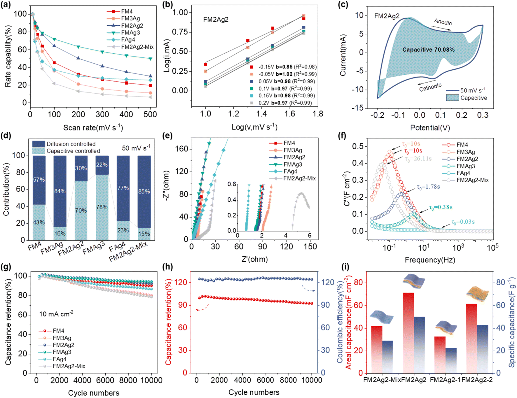 | ||
| Fig. 5 (a) Rate capability of TOCNFs/Ti3C2Tx/AgNW hybrid films based on GCD profiles. (b) Linear relationship of the current (i) and the scan rate (v) of FM2Ag2. (c) Surface capacitance contribution to the total charge storage at 50 mV s−1 for FM2Ag2. (d) Contribution of the capacitive and diffusion-controlled current of TOCNFs/Ti3C2Tx/AgNW hybrid films at 50 mV s−1. (e) Nyquist plots. (f) Progression of the imaginary (C′′) parts of the areal capacitance as a function of frequency. (g) Long-term cycling performance of TOCNFs/Ti3C2Tx/AgNW hybrid films at 10 mA cm−2. (h) Long-term cycling performance and corresponding coulombic efficiency of FM2Ag2 at 10 mA cm−2, and (i) areal capacitance and specific capacitance of FM2Ag2 hybrid films compared with other different structures. | ||
Kinetic analysis of the film electrodes was performed to elucidate the electrochemical energy storage mechanism. The electrochemical energy storage of the electrode could be divided into embedded pseudocapacitance contributed by diffusion-controlled ion deintercalation and surface capacitance contributed by non-diffusion.17,81 Because there were no obvious redox peaks in the CV curves, the scan rate and current magnitude were analyzed at the selected potentials of −0.15, −0.05, 0.05, 0.1, 0.15, and 0.2 V. According to formulas (15) and (16), b can be obtained by linear fitting of logi–logv. During the electrochemical reaction, the transfer of surface reactive ions is linear with v, whereas the migration of ions during diffusion is linear with v1/2.81,82 After fitting the logi–logv curves, the corresponding b values were obtained, as shown in Fig. 5b and S22a–e.† For the FM2Ag2 electrode, the corresponding b values were 0.85, 1.02, 0.98, 0.97, 0.98, and 0.97 (R2 = 0.99), indicating that the charge storage is mainly attributed to the contribution of the surface capacitance. At a scan rate of 50 mV s−1, the ratio of the surface capacitance contribution of the electrode was determined according to eqn (15) (Fig. 5c, d and S22f–j†). The calculated ratios for different electrodes were 43%, 16%, 70%, 78%, 23%, and 15%, revealing the main capacitive behavior of FM2Ag2 and FMAg3 for charge storage. These results are consistent with those obtained for the rate capability (Fig. 5a).
Electrochemical impedance spectroscopy (EIS) measurements were conducted between 0.01 Hz and 100 kHz to elucidate the kinetics of ion transport in the electrode (Fig. 5e). Directly mixing TOCNFs with conductive components resulted in an obvious increase in the ion transport resistance of electrodes, as analyzed from the Nyquist plots. The TOCNFs/Ti3C2Tx/AgNW hybrid films showed an almost vertical rise in the imaginary impedance (at low frequencies). This indicates that electrolyte ions are easily accessible to charge-storage sites on the surfaces.12,83 Consistent with a previous study, FM2Ag2 exhibited a double-layer capacitive behavior. This may be due to the optimal specific surface area and interlayer space between the AgNWs and Ti3C2Tx nanosheets, which reduced the charge-diffusion resistance. Compared with other layered films obtained by filtration, FM2Ag2-mix exhibited the highest equivalent series resistance (4.5 Ω). However, the biomimetic design of the conductive layers gave rise to lower equivalent series resistance and better charge transfer kinetics in the sandwich-structured films, making it easier for the transport of electrolyte ions. The internal resistance of the FM2Ag2 film electrode was approximately 1.6 Ω. The real (C′) and imaginary (C′′) capacitances of these electrode films are plotted versus the frequency in Fig. 5f and S23.† The relaxation time constant (τ0) of FM2Ag2-mix was significantly higher than those of the other films. The τ0 values of the other electrodes decreased with the decrease in Ti3C2Tx contents. The relaxation time of FM2Ag2 was 1.78 s. This confirms our previous results that the ion mobility rate is the main factor limiting the rate performance (Fig. 5a). When Ti3C2Tx nanosheet contents were low, the ions in the electrolyte easily diffused and migrated into the electrode. In contrast, the diffusion path of ions was longer for high-loading nanosheets, and thus the ions in the electrolyte could not be reached at high scanning speeds. This impeded some active surfaces to participate in redox reactions to store charges, which in turn degraded the electrode rate capability. As shown in Fig. 5g, galvanostatic charge–discharge tests over 10000 cycles were performed at 10 mA cm−2 to reveal the electrochemical stability and capacitance retention of all the prepared electrodes. Before 400 cycles, the capacitance performance improved. This is because of the gradual infiltration of electrolytes in the electrode and activation of electrode materials. After 10000 cycles, FM3Ag and FM2Ag2 exhibited high electrochemical stability and capacitance retentions of 94.29% and 92.39%, respectively. However, the capacitance retention of FM2Ag2-mix significantly decreased to 78.57%. In addition, capacitance decay was accelerated, owing to the increase in resistance, which dissipated more energy, resulting in thermal loss and lower capacitance.17 FM2Ag2 achieved superb specific/areal capacitance and long-term stability owing to fast ion transport toward redox-active sites and high electron transfer rates in the 3D porous structure with optimal layer spacing. Typical GCD curves of FM2Ag2 reveal that the coulombic efficiency was 124.1% (Fig. 5h), suggesting its highly reversible capacitance behavior and fewer parasitic reactions.84 These properties were better than those of most MXene- and silver-based electrode materials (Table S3†), confirming their potential applications in supercapacitors. More importantly, we compared FM2Ag2 with other structures (Fig. 5i), including a homogeneously mixed structure, two layer structure, and sandwich structures with the conductive layer in the middle covered by TOCNF layers on both sides. FM2Ag2 showed better performance in terms of areal and specific capacitance.
Surface wettability is an important parameter in the development of high-performance supercapacitors. Non-uniform and insufficient wetting leads to an inhomogeneous distribution of the current density.85 All hybrid films show good hydrophilicity (Fig. S24†). With the decrease in MXene nanosheets, the hydrophilicity gradually decreased, and the contact angle increased from 54.6 ± 3.5° to 76.5 ± 2.8°. Moreover, the contact angle of FM2Ag2 was 62.3 ± 3.1°, higher than that of the homogeneously mixed films (51° ± 2.5°).
4 Conclusions
In summary, we developed a facile micro/nanoscale strategy to fabricate ultrathin, strong, flexible, and high-conductivity TOCNFs/Ti3C2Tx/AgNW hybrid films with a sandwich structure using a vacuum-assisted filtration method. The combination of Ti3C2Tx MXene and AgNWs mimicked a leaf-like nanostructure, in which 1D AgNWs acted as a conductive skeleton (vein) and 2D MXene acted as a connection (lamina), leading to a continuous and highly conductive 3D network. The introduction of TOCNFs as an interlayer not only endowed the hybrid films with excellent mechanical properties but also avoided the negative effect on the electrical conductivity caused by the insulating nature of the TOCNFs. These factors synergistically contributed to excellent EMI shielding and electrochemical properties. The obtained FM2Ag2 film (∼4 μm in thickness and up to 1.29 × 10⁷ S m−1 in conductivity) exhibited a high areal and specific capacitance of 110.7 mF cm−2 and 77.6 F g−1 at 10 mV s−1, respectively, and excellent stability with 92.4% capacitance retention after 10000 cycles, while maintaining a high EMI shielding effectiveness of 28016.2 dB cm2 g−1. The proposed hierarchical structure strategy will give insight into the construction of high-performance films from the perspective of multiscale design and can significantly improve the practical applications of these materials in wearable or portable electronic devices.
Author contributions
Beibei Wang: methodology, investigation, writing-reviewing, and editing. Weiye Zhang and Jingmeng Sun: conceptualization and investigation. Chenhuan Lai: writing-original draft preparation. Shengbo Ge: data curation. Hongwu Guo and Yi Liu: methodology, supervision, and resources. Daihui Zhang: methodology, conceptualization, and supervision.Conflicts of interest
There are no conflicts to declare.Acknowledgements
This research was funded by the National Natural Science Foundation of China (32001283, 32271809, and 31890774), Natural Science Foundation of Beijing Municipality (6184045), National Key R&D Program of China (2017YFD0601104), and Fundamental Research Funds for the Central Universities (2018ZY12). The authors would like to thank Kehui Han from Shiyanjia Lab (https://www.shiyanjia.com) for the XPS tests, and Yanhua Wu from Scientific Research N Power (https://www.yanbotimes.cn) for the micromechanical tests.References
- P. He, Z. Liu, G. Mao, Q. Liu, M. Zheng, R. Zuo, W. Cao, Z. Hou, J. Yuan and M. Cao, Composites, Part A, 2022, 157, 106935 CrossRef CAS.
- Z. Liu, T. Zhu, J. Wang, Z. Zheng, Y. Li, J. Li and Y. Lai, Nano-Micro Lett., 2022, 14, 61 CrossRef CAS PubMed.
- Z. Wang, Y. H. Lee, S. W. Kim, J. Y. Seo, S. Y. Lee and L. Nyholm, Adv. Mater., 2021, 33, 2000892 CrossRef CAS PubMed.
- N. Siraj, S. Macchi, B. Berry and T. Viswanathan, Electrochem, 2020, 1, 410–438 CrossRef.
- D. Zhao, Y. Zhu, W. Cheng, W. Chen, Y. Wu and H. Yu, Adv. Mater., 2021, 33, 2000619 CrossRef CAS PubMed.
- E. Zhu, K. Pang, Y. Chen, S. Liu, X. Liu, Z. Xu, Y. Liu and C. Gao, Sci. China Mater., 2022, 66(3), 1106–1113 Search PubMed.
- M. Han, C. E. Shuck, R. Rakhmanov, D. Parchment, B. Anasori, C. M. Koo, G. Friedman and Y. Gogotsi, ACS Nano, 2020, 14, 5008–5016 CrossRef CAS PubMed.
- T. Yun, H. Kim, A. Iqbal, Y. S. Cho, G. S. Lee, M. K. Kim, S. J. Kim, D. Kim, Y. Gogotsi, S. O. Kim and C. M. Koo, Adv. Mater., 2020, 32, 1906769 CrossRef CAS PubMed.
- Z. Xiang, Y. Shi, X. Zhu, L. Cai and W. Lu, Nano-Micro Lett., 2021, 13, 150 CrossRef CAS PubMed.
- W. Chen, L. Liu, H. Zhang and Z. Yu, ACS Nano, 2020, 14, 16643–16653 CrossRef CAS PubMed.
- M. Jin, W. Chen, L. Liu, H. Zhang, L. Ye, P. Min and Z. Yu, J. Mater. Chem. A, 2022, 10, 14364–14373 RSC.
- W. Tian, A. VahidMohammadi, M. S. Reid, Z. Wang, L. Ouyang, J. Erlandsson, T. Pettersson, L. Wågberg, M. Beidaghi and M. M. Hamedi, Adv. Mater., 2019, 31, 1902977 CrossRef PubMed.
- J. Liu, L. Mckeon, J. Garcia, S. Pinilla, S. Barwich, M. Mobius, P. Stamenov, J. N. Coleman and V. Nicolosi, Adv. Mater., 2022, 34, e2106253 CrossRef PubMed.
- X. Chia and M. Pumera, Nat. Catal., 2018, 1, 909–921 CrossRef CAS.
- H. Liu, Z. Huang, T. Chen, X. Su, Y. Liu and R. Fu, Chem. Eng. J., 2022, 427, 131540 CrossRef CAS.
- J. Zhao, Q. Li, T. Shang, F. Wang, J. Zhang, C. Geng, Z. Wu, Y. Deng, W. Zhang, Y. Tao and Q. Yang, Nano Energy, 2021, 86, 106091 CrossRef CAS.
- L. Li, N. Zhang, M. Zhang, L. Wu, X. Zhang and Z. Zhang, ACS Sustain. Chem. Eng., 2018, 6, 7442–7450 CrossRef CAS.
- S. Tang, Z. Wu, X. Li, F. Xie, D. Ye, E. Ruiz-Hitzky, L. Wei and X. Wang, Carbohydr. Polym., 2023, 299, 120204 CrossRef CAS PubMed.
- H. Cheng, Y. Pan, Q. Chen, R. Che, G. Zheng, C. Liu, C. Shen and X. Liu, Adv. Compos. Hybrid Mater., 2021, 4, 505–513 CrossRef CAS.
- X. Peng, K. Dong, C. Ye, Y. Jiang, S. Zhai, R. Cheng, D. Liu, X. Gao, J. Wang and Z. L. Wang, Sci. Adv., 2020, 6, a9624 CrossRef PubMed.
- A. Brakat and H. Zhu, Nano-Micro Lett., 2021, 13, 94 CrossRef CAS PubMed.
- J. Liu, Z. Liu, H. B. Zhang, W. Chen, Z. Zhao, Q. W. Wang and Z. Z. Yu, Adv. Electron. Mater., 2020, 6, 1901094 CrossRef CAS.
- B. Wang, Y. Li, W. Zhang, J. Sun, J. Zhao, Y. Xu, Y. Liu, H. Guo and D. Zhang, Carbohydr. Polym., 2022, 286, 119302 CrossRef CAS PubMed.
- W. Liu, K. Liu, H. Du, T. Zheng, N. Zhang, T. Xu, B. Pang, X. Zhang, C. Si and K. Zhang, Nano-Micro Lett., 2022, 14(6), 323–349 Search PubMed.
- G. S. Lee, T. Yun, H. Kim, I. H. Kim, J. Choi, S. H. Lee, H. J. Lee, H. S. Hwang, J. G. Kim, D. Kim, H. M. Lee, C. M. Koo and S. O. Kim, ACS Nano, 2020, 14, 11722–11732 CrossRef CAS PubMed.
- Q. Lin, R. Gao, D. Li, Y. Lu, S. Liu, Y. Yu, Y. Huang and W. Yu, npj Flexible Electron., 2022, 6, 13 CrossRef CAS.
- J. Jian, Y. Xie, S. Gao, Y. Sun, C. Lai, J. Wang, C. Wang, F. Chu and D. Zhang, Carbohyd. Polym., 2022, 294, 119760 CrossRef CAS PubMed.
- Z. Ling, J. Chen, X. Wang, L. Shao, C. Wang, S. Chen, J. Guo and Q. Yong, Carbohydr. Polym., 2022, 296, 119920 CrossRef CAS PubMed.
- G. Jia, J. Plentz, A. Dellith, C. Schmidt, J. Dellith, G. Schmidl and G. Andra, Nano-Micro Lett., 2020, 12, 19 CrossRef CAS PubMed.
- M. Hua, S. Wu, Y. Ma, Y. Zhao, Z. Chen, I. Frenkel, J. Strzalka, H. Zhou, X. Zhu and X. He, Nature, 2021, 590, 594–599 CrossRef CAS PubMed.
- Y. Xie, S. Gao, Z. Ling, C. Lai, Y. Huang, J. Wang, C. Wang, F. Chu, F. Xu, M. Dumont and D. Zhang, J. Mater. Chem. A, 2022, 10, 13685–13696 RSC.
- B. Zhou, Q. Li, P. Xu, Y. Feng, J. Ma, C. Liu and C. Shen, Nanoscale, 2021, 13, 2378–2388 RSC.
- Z. Ma, S. Kang, J. Ma, L. Shao, Y. Zhang, C. Liu, A. Wei, X. Xiang, L. Wei and J. Gu, ACS Nano, 2020, 14, 8368–8382 CrossRef CAS PubMed.
- L. X. Liu, W. Chen, H. B. Zhang, Q. W. Wang, F. Guan and Z. Z. Yu, Adv. Funct. Mater., 2019, 29, 1905197 CrossRef CAS.
- M. Miao, R. Liu, S. Thaiboonrod, L. Shi, S. Cao, J. Zhang, J. Fang and X. Feng, J. Mater. Chem. C, 2020, 8, 3120–3126 RSC.
- C. Shao, H. Chang, M. Wang, F. Xu and J. Yang, ACS Appl. Mater. Interfaces, 2017, 9, 28305–28318 CrossRef CAS PubMed.
- S. Dai, Y. Chu, D. Liu, F. Cao, X. Wu, J. Zhou, B. Zhou, Y. Chen and J. Huang, Nat. Commun., 2018, 9, 2737 CrossRef PubMed.
- C. F. Zhang, B. Anasori, A. Seral-Ascaso, S. H. Park, N. McEvoy, A. Shmeliov, G. S. Duesberg, J. N. Coleman, Y. Gogotsi and V. Nicolosi, Adv. Mater., 2017, 29(36), 1702678 CrossRef PubMed.
- F. Shahzad, M. Alhabeb, C. B. Hatter, B. Anasori, H. S. Man, C. M. Koo and Y. Gogotsi, Science, 2016, 353, 1137–1140 CrossRef CAS PubMed.
- M. Alhabeb, K. Maleski, B. Anasori, P. Lelyukh, L. Clark, S. Sin and Y. Gogotsi, Chem. Mater., 2017, 29, 7633–7644 CrossRef CAS.
- R. M. Simon, Polym.-Plast. Technol. Eng., 1981, 17, 1–10 CrossRef CAS.
- A. Iqbal, F. Shahzad, K. Hantanasirisakul, M. Kim, J. Kwon, J. Hong, H. Kim, D. Kim, Y. Gogotsi and C. M. Koo, Science, 2020, 369, 446–450 CrossRef CAS PubMed.
- C. Liang, Z. Wang, L. Wu, X. Zhang, H. Wang and Z. Wang, ACS Appl. Mater. Interfaces, 2017, 9, 29950–29957 CrossRef CAS PubMed.
- Z. Chen, C. Xu, C. Ma, W. Ren and H. Cheng, Adv. Mater., 2013, 25, 1296–1300 CrossRef CAS PubMed.
- Z. Zeng, H. Jin, M. Chen, W. Li, L. Zhou and Z. Zhang, Adv. Funct. Mater., 2016, 26, 303–310 CrossRef CAS.
- M. Ghidiu, M. R. Lukatskaya, M. Q. Zhao, Y. Gogotsi and M. W. Barsoum, Nature, 2014, 516, 78–81 CrossRef CAS PubMed.
- P. L. Taberna, P. Simon and J. F. Fauvarque, J. Electrochem. Soc., 2003, 150, A292–A300 CrossRef CAS.
- X. Xu, K. Wang, Y. Zhou, C. Lai, D. Zhang, C. Xia and A. Pugazhendhi, Fuel, 2023, 338, 127361 CrossRef CAS.
- K. Wang, S. Gao, C. Lai, Y. Xie, Y. Sun, J. Wang, C. Wang, Q. Yong, F. Chu and D. Zhang, Ind. Crops Prod., 2022, 187, 115366 CrossRef CAS.
- S. Hou, B. Shen, D. Zhang, R. Li, X. Xu, K. Wang, C. Lai and Q. Yong, Bioresour. Technol., 2022, 362, 127825 CrossRef CAS PubMed.
- R. Sun, H. Zhang, J. Liu, X. Xie, R. Yang, Y. Li, S. Hong and Z. Yu, Adv. Funct. Mater., 2017, 27, 1702807 CrossRef.
- S. Chen, Y. Xiang, W. Xu and C. Peng, Inorg. Chem. Front., 2019, 6, 199–208 RSC.
- W. Shao, M. Tebyetekerwa, I. Marriam, W. Li, Y. Wu, S. Peng, S. Ramakrishna, S. Yang and M. Zhu, J. Power Sources, 2018, 396, 683–690 CrossRef CAS.
- X. Zhu, B. Liu, H. Hou, Z. Huang, K. M. Zeinu, L. Huang, X. Yuan, D. Guo, J. Hu and J. Yang, Electrochim. Acta, 2017, 248, 46–57 CrossRef CAS.
- B. Wang, X. Wang, Y. Liu, Q. Zhang, G. Yang, D. Zhang and H. Guo, Polym. Degrad. Stab., 2023, 110269 CrossRef CAS.
- X. Liu, K. Pang, Y. Liu, C. Gao and Z. Xu, ACS Nano, 2021, 9, 14703–14712 Search PubMed.
- Y. Zhang, K. Ruan and J. Gu, Small, 2021, 17, 2101951 CrossRef CAS PubMed.
- D. Zhang, J. Jian, Y. Xie, S. Gao, Z. Ling, C. Lai, J. Wang, C. Wang, F. Chu and M. Dumont, Chem. Eng. J., 2022, 427, 130921 CrossRef CAS.
- X. Xu, D. Zhang, K. Wang, Y. Jia, C. Yang, B. Shen, C. Lai and Q. Yong, Bioresour. Technol., 2022, 344, 126315 CrossRef CAS PubMed.
- Y. Xie, S. Gao, J. Jian, X. Shi, C. Lai, C. Wang, F. Xu, F. Chu and D. Zhang, Int. J. Biol. Macromol., 2023, 227, 462–471 CrossRef CAS PubMed.
- C. Wang, J. Xu, S. Ke, Y. Li, X. Zhu, X. Gu, C. Kan and D. Shi, ACS Appl. Nano Mater., 2020, 3, 10844–10854 CrossRef CAS.
- S. Wan, X. Li, Y. Chen, N. Liu, Y. Du, S. Dou, L. Jiang and Q. Cheng, Science, 2021, 374, 96–99 CrossRef CAS PubMed.
- P. Sambyal, A. Iqbal, J. Hong, H. Kim, M. Kim, S. M. Hong, M. Han, Y. Gogotsi and C. M. Koo, ACS Appl. Mater. Interfaces, 2019, 11, 38046–38054 CrossRef CAS PubMed.
- W. Yang, Z. Zhao, W. Kai and R. Huang, J. Mater. Chem. C, 2017, 5, 3748–3756 RSC.
- M. Miao, R. Liu, S. Thaiboonrod, L. Shi, S. Cao, J. Zhang, J. Fang and X. Feng, J. Mater. Chem. C, 2020, 8, 3120–3126 RSC.
- Y. Zhang, K. Ruan, K. Zhou and J. Gu, Adv. Mater., 2023, e2211642 CrossRef PubMed.
- Y. Guo, H. Qiu, K. Ruan, Y. Zhang and J. Gu, Nano-Micro Lett., 2022, 14(2), 94–106 CrossRef PubMed.
- Y. Han, K. Ruan and J. Gu, Nano Res., 2022, 15, 4747–4755 CrossRef CAS.
- K. Qian, S. Li, J. Fang, Y. Yang, S. Cao, M. Miao and X. Feng, J. Mater. Sci. Technol., 2022, 127, 71–77 CrossRef.
- A. Iqbal, P. Sambyal and C. M. Koo, Adv. Funct. Mater., 2020, 30, 2000883 CrossRef CAS.
- Y. Zhang, Z. Ma, K. Ruan and J. Gu, Nano Res., 2022, 15, 5601–5609 CrossRef CAS.
- X. Feng, J. Ning, B. Wang, H. Guo, M. Xia, D. Wang, J. Zhang, Z. Wu and Y. Hao, Nano Energy, 2020, 72, 104741 CrossRef CAS.
- X. Li, W. You, L. Wang, J. Liu, Z. Wu, K. Pei, Y. Li and R. Che, ACS Appl. Mater. Interfaces, 2019, 11, 44536–44544 CrossRef CAS PubMed.
- E. Kim, B. Lee, K. Maleski, Y. Chae, Y. Lee, Y. Gogotsi and C. W. Ahn, Nano Energy, 2021, 81, 105616 CrossRef CAS.
- S. Kim, H. Gang, G. Park, H. Jeon and Y. G. Jeong, Adv. Eng. Mater., 2021, 23, 2100548 CrossRef CAS.
- M. A. Hope, A. C. Forse, K. J. Griffith, M. R. Lukatskaya, M. Ghidiu, Y. Gogotsi and C. P. Grey, Phys. Chem. Chem. Phys., 2016, 18, 5099–5102 RSC.
- M. R. Lukatskaya, S. Bak, X. Yu, X. Yang, M. W. Barsoum and Y. Gogotsi, Adv. Energy Mater., 2015, 5, 1500589 CrossRef.
- N. Agmon, Chem. Phys. Lett., 1995, 244, 456–462 CrossRef CAS.
- W. Gao, N. Singh, L. Song, Z. Liu, A. L. M. Reddy, L. Ci, R. Vajtai, Q. Zhang, B. Wei and P. M. Ajayan, Nat. Nanotechnol., 2011, 6, 496–500 CrossRef CAS PubMed.
- J. Tang, T. Mathis, X. Zhong, X. Xiao, H. Wang, M. Anayee, F. Pan, B. Xu and Y. Gogotsi, Adv. Energy Mater., 2021, 11, 2003025 CrossRef CAS.
- J. Wang, J. Polleux, J. Lim and B. Dunn, J. Phys. Chem. C, 2007, 111, 14925–14931 CrossRef CAS.
- V. Augustyn, J. Come, M. A. Lowe, J. W. Kim, P. L. Taberna, S. H. Tolbert, H. D. Abruna, P. Simon and B. Dunn, Nat. Mater., 2013, 12, 518–522 CrossRef CAS PubMed.
- J. Wu, Q. Li, C. E. Shuck, K. Maleski, H. N. Alshareef, J. Zhou, Y. Gogotsi and L. Huang, Nano Res., 2022, 15, 535–541 CrossRef.
- M. Ghidiu, M. R. Lukatskaya, M. Q. Zhao, Y. Gogotsi and M. W. Barsoum, Nature, 2014, 516, 78–81 CrossRef CAS PubMed.
- D. H. Jeon, Energy Storage Mater., 2019, 18, 139–147 CrossRef.
Footnote |
| † Electronic supplementary information (ESI) available. See DOI: https://doi.org/10.1039/d3ta00442b |
| This journal is © The Royal Society of Chemistry 2023 |