High performance ambipolar organic field-effect transistors based on indigo derivatives†
Received
17th July 2014
, Accepted 14th September 2014
First published on 17th September 2014
Abstract
A bio-inspired organic semiconductor 5,5′-diphenylindigo shows excellent and well-balanced ambipolar transistor properties; its hole and electron mobilities are 0.56 and 0.95 cm2 V−1 s−1, respectively. The enhanced performance is attributed to the extended π–π overlap of the phenyl groups as well as the characteristic packing pattern that is a hybrid of the herringbone and brickwork structures. The ambipolar transistor characteristics are analyzed considering its operating regions, where a large unipolar saturated region appears due to the difference of the electron and hole threshold voltages.
Introduction
Development of ambipolar organic semiconductors capable of both hole and electron transports has essential importance in designing electronic and optoelectronic organic devices.1,2 Recently, high-performance ambipolar transistors have been realized in donor–acceptor polymers;1–6 examples are a polymer consisting of thiophene and diketopyrrolopyrole (DPP), showing the hole and electron field-effect mobilities of μh/μe = 0.9/0.1 cm2 V−1 s−1,7 and a polymer of thienothiophene and DPP (μh/μe = 1.36/1.56 cm2 V−1 s−1).8 Ambipolar transport has been also achieved in some small-molecule organic semiconductors such as quinoidal oligothiophenes,9–11 fullerenes,12,13 phthalocyanines,14–18 metal complexes,19 and even pentacene.16,20 However, ambipolar transport is sometimes sensitive to conditions such as annealing and oxygen exposure,9,10,12,13 and the performance drops by several orders in comparison with the unipolar operation. Among these materials, μh/μe = 3/3 cm2 V−1 s−1 has been reported in a pentacene ambipolar transistor,20 but mobilities of other small-molecule ambipolar transistors are still lower than 1 cm2 V−1 s−1. It has been recognized that stable ambipolar operation is realized by the appropriate choice of passivation layers; in particular tetratetracontane (TTC, C44H90) is an excellent passivation material,14–16,21 though the operation still depends on the choice of the contact metals.16,19,21,22
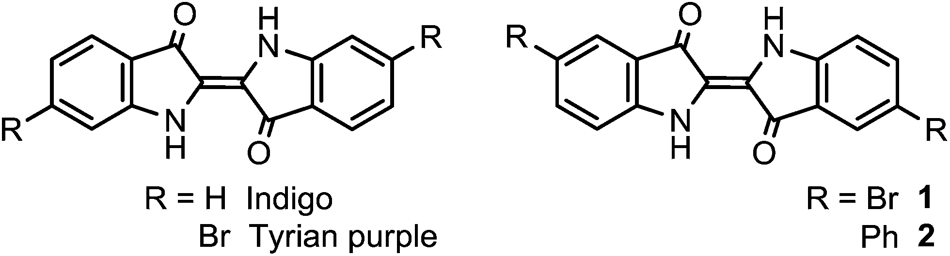
Recently, ambipolar operation has been reported in indigo derivatives (Scheme 1).23 Indigo is a plant-origin dye produced from Indigofera tinctoria and Isatis tintora, which have been cultivated for at least four thousand years for coloring textiles.24 Indigo shows a very high melting point (390–392 °C) and an extremely low solubility in common organic solvents, explained by stabilization from the inter- and intramolecular hydrogen bonds. Intermolecular interactions of the π-skeletons also strongly influence the charge transport in indigo thin films. Indigo shows ambipolar transport with well-balanced mobilities μh/μe = 0.01/0.01 cm2 V−1 s−1 and good stability against degradation in air.23 Tyrian purple (6,6′-dibromoindigo, Scheme 1) shows ambipolar transport with μh/μe = 0.4/0.4 cm2 V−1 s−1 as well.24,25 Very recently, transistor properties of several halogen-substituted indigos have been reported, where 6,6′-dichloroindigo shows μh/μe = 1.8–2.1 × 10⁻³/7–9 × 10−3 cm2 V−1 s−1, and 5,5′-dibromoindigo (1) shows only n-type transport: μe = 2–4.1 × 10⁻⁵ cm2 V−1 s−1.26 These molecules are of interest not only as biological and bio-inspired materials but also because of their minimal molecular structure consisting of electron-donating nitrogen atoms working as donors and electron-withdrawing carbonyl groups as acceptors.27 The characteristic blue colour comes from the small energy gap, and the resulting long-wavelength absorption is closely related to the ambipolar transport.
 |
| | Scheme 1 Structures of indigo derivatives. | |
In the present work, in order to improve the performance of indigo semiconductors, we investigate indigo derivatives substituted at the 5-position instead of the 6-position in Tyrian purple, namely 5,5′-dibromoindigo (1) and 5,5′-diphenylindigo (2) (Scheme 1). It is a conventional way in organic semiconductors to extend the π-skeleton by connecting phenyl groups to achieve a more parallel molecular packing.28,29 In addition, substitutions at the 5,5′-positions lead to a bathochromic shift in contrast to the 6,6′-substitutions.26,27,30 We have found that the 5-bromo and 6-bromo indigo derivatives have basically the same molecular packing as the parent indigo, whereas the 5-phenyl indigo has a new type of molecular packing that is a hybrid of the herringbone and brickwork packings, and exhibits an improved transistor performance. In order to analyze the ambipolar transistor characteristics, operating regions of ambipolar transistors are investigated. Since there is a considerable difference between the hole and electron threshold voltages, a large unipolar saturated region appears. We have also fabricated an ambipolar transistor of 2 on an organic substrate, polyethylenenaphtalate (PEN), where polychloroparaxylylene (parylene C) is proved to be an inert enough gate dielectric to achieve ambipolar transport.
Results and discussion
Preparation and electrochemical properties
Although 1 and 2 were reported before the era of the coupling reaction,31,32 we obtained 2 using the standard coupling reaction. Compounds 1 and 2 were prepared from the commercially available bromoindole similarly to the published procedures,33–35 and purified several times by temperature gradient sublimation.
The electronic structures are investigated by cyclic voltammetry (CV) and ultraviolet-visible spectroscopy (UV-vis). The CV shows both oxidation and reduction peaks. The highest occupied molecular orbital (HOMO) level is estimated from the oxidation potential, Eox, and the lowest unoccupied molecular orbital (LUMO) level is obtained from the reduction potential, Ered (Table 1). The resulting HOMO–LUMO gaps of 1 and 2 are 1.79 and 1.65 eV, respectively. From the absorption edges, the energy gaps are also estimated to be 1.70 eV for 1 and 1.70 eV for 2 (Table 1). These values are in good agreement with the reported values in indigo, which are estimated to be 1.7 eV both from CV and from the absorption edge.23,26 The absorption of 2 is not much different from that of 1, suggesting that the π-skeleton is not really extended because, as will be verified from the crystal structure, the phenyl rings are not coplanar to the indigo part. It has been reported that hole transport is realized for Au electrodes when the HOMO is located above 5.6 eV, and electron transport is achieved when the LUMO level is located deeper than 3.15 eV.36 The estimated HOMO–LUMO levels of the present compounds satisfy these conditions.
Table 1 Redox potentials and energy levels of 1, 2, and the parent indigoa
| Compounds |
E
ox [V] |
E
red [V] |
HOMO [eV] |
LUMO [eV] |
HOMO–LUMO gap [eV] |
Optical gap [eV] |
| Solution |
Film |
|
Onset redox potential vs. Fc/Fc+ is assumed to be 4.8 eV from the vacuum level.36
|
|
1
|
0.85 |
−0.94 |
5.65 |
3.86 |
1.79 |
1.89 |
1.70 |
|
2
|
0.76 |
−0.89 |
5.56 |
3.91 |
1.65 |
1.85 |
1.70 |
| Indigo |
0.80 |
−0.89 |
5.60 |
3.91 |
1.69 |
1.9 (ref. 23) |
1.7 (ref. 23) |
Operating regions of ambipolar transistors
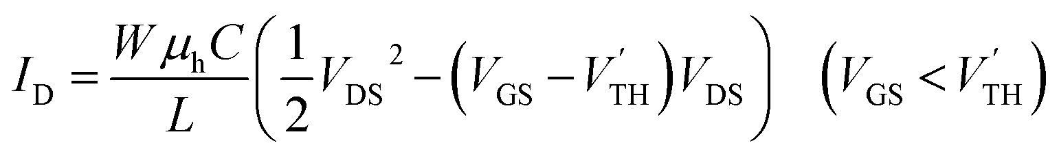
Although a unipolar saturated region does not appear in the ordinary formulae of ambipolar transistors,1,19 in general a considerable unipolar saturated region appears due to the difference between the electron (VTH) and hole (V′TH) threshold voltages. When VTH and V′TH are nonzero, the operating regions are divided as shown in Fig. 1. This figure is depicted for V′TH < 0 < VTH, but VTH and V′TH may have the same sign; in this case the whole figure is translated horizontally. The transistor characteristics are obtained assuming the gradual channel approximation (ESI†). When we follow the line (i) from right to left, the linear region (L) in VGS − VTH > VDS,| |  | (1) |
is followed by the unipolar electron-transporting saturated region (S),| | 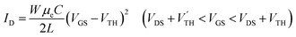 | (2) |
at VGS = VDS + VTH. An ambipolar region (A) appears below VGS = VDS + V′TH,| |  | (3) |
which is certainly continuous to eqn (2) at VGS = VDS + V′TH. This is connected to the unipolar hole-transporting saturated region (S′) below VGS < VTH,| |  | (4) |
where the first term of eqn (3) vanishes. Finally, a reversed hole-transporting linear region (L′) appears below VGS < V′TH,| | 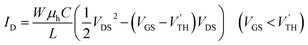 | (5) |
which is continuous to eqn (4) at VGS = V′TH. Regions appear successively as L → S → A → S′ → L′, in which ID follows VGS2 in the central S, A, and S′ regions, whereas ID depends on VGS linear in the L and L′ regions.
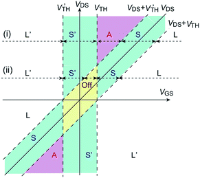 |
| | Fig. 1 Operating regions of ambipolar transistors considering nonzero threshold voltages. | |
Below VDS < VTH − V′TH, an off state appears, where ID drops to zero. When we trace the horizontal line (ii) in Fig. 1, regions appear successively as L → S → off → S′ → L′. Similar relationships hold for hole transport, and the lower half of Fig. 1 has a similar shape to the upper half. The off region is represented by the rhombic domain in Fig. 1, and the ambipolar region appears only above VDS > VTH − V′TH; this is the reason that ambipolar characteristics are observed only at comparatively large VDS in the actual ambipolar transistors. The off region appears in V′TH < VGS < VTH at VDS = 0 V, but transistor characteristics are not observed at this VDS = 0 V limit, and the actual ID = 0 region is always smaller than VTH − V′TH. The ambipolar region is sandwiched by the unipolar saturated regions, whose widths are again VTH − V′TH. It is therefore appropriate to extract the mobility from the formula of the unipolar saturated region (eqn (2) and (4)). Even in the conventional unipolar transistors, we should pay attention for VGS not to exceed VDS in order to keep the transfer characteristics in the saturated region. In contrast, VTH – V′TH is larger than VDS in many ambipolar transistors. It is also noteworthy that both the electron and hole sides have the same importance whatever the VDS sign is. We should be cautious to extract VTH and V′TH from the experimental data, because the apparent threshold voltages extracted from the transfer characteristics are dependent on VDS and different from the intrinsic threshold voltages, VTH and V′TH.
Transistor characteristics
Transistors with bottom-gate top-contact configuration were prepared by using a heavily doped n-type Si wafer with 300 nm SiO2 as the gate insulator (Fig. 2). It has been recognized that in organic transistors, not only the electrode but also treatment of the semiconductor/insulator interface is important to determine the charge carrier types. In order to achieve ambipolar charge carrier transport, it is effective to treat the substrate with an appropriate passivation layer. In particular, tetratetracontane (TTC, C44H90) has been proved to be useful to realize the ambipolar transport.14–16,23–25 TTC is a long-chain alkane molecule that has an advantage of the low dielectric constant and the reduced polarization effect. At the same time, the high surface energy increases the crystallinity of the semiconductor layer to improve the charge transport properties.14–16
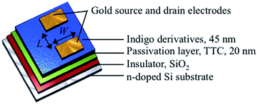 |
| | Fig. 2 Structure of an indigo field-effect transistor in bottom-gate top-contact geometry, where L and W are 100 and 1000 μm, respectively. | |
Transfer and output transistor characteristics measured under vacuum show well-balanced electron and hole transports (Fig. 3). The cusp of the transfer characteristics, which corresponds to the charge neutrality point in graphene transistors, is not much deviated from the zero gate voltage (VGS = 0 V). Although 1 shows a considerable off region, 2 shows a comparatively sharp charge neutrality point. Threshold voltages listed in Table 2 are extracted from the square root ID plot of the transfer characteristics. The values for 1 do not strictly follow the expectation from Fig. 1, but agree with the results of the output characteristics; in Fig. 3b, electron conductance at VGS = 0 V starts to increase around VDS = −60 V, and hole conductance at VGS = 0 V in Fig. 3c increases from VDS = 40 V. From Fig. 1, this indicates VTH = 60 V and V′TH = −40 V. For 2, the threshold voltages when VGS and VDS have the same sign directly afford VTH = 73 V and V′TH = −60 V. The start of the reversed region is not obvious at VGS = 0 V in the output characteristics (Fig. 3e and f), because the threshold values are comparatively large. It is also because VTH − V′TH is as large as 133 V that the transfer characteristics (Fig. 3) show VGS2 dependence rather than VGS linear dependence. Fig. 1 demonstrates that the saturated region continues at most in this voltage extent starting from the apparent threshold voltage.
 |
| | Fig. 3 (a) Transfer characteristics of thin-film transistors of 1. (b) Output characteristics at VDS < 0, and (c) at VDS > 0. (d) Transfer characteristics of thin-film transistors of 2. (e) Output characteristics at VDS < 0, and (f) at VDS > 0. All measurements are carried out under vacuum. | |
Table 2 Summary of mobilities of 1, 2, indigo and Tyrian purple
| Compound |
V
DS [V] |
Maximum mobilities under vacuum [cm2 V−1 s−1] |
Average mobilities under vacuum [cm2 V−1 s−1] |
Threshold voltage [V] |
| Hole |
Electron |
Hole |
Electron |
Hole |
Electron |
|
1
|
80 |
0.21 |
0.04 |
0.08 |
0.03 |
−58 |
71 |
| −80 |
0.07 |
0.35 |
0.02 |
0.27 |
−31 |
97 |
|
2
|
80 |
0.56 |
0.60 |
0.42 |
0.49 |
−31 |
73 |
| −80 |
0.24 |
0.95 |
0.16 |
0.73 |
−60 |
29 |
| Indigo23 |
10 |
0.01 |
0.01 |
— |
— |
— |
— |
| Tyrian purple24 |
12 |
0.4 |
0.4 |
— |
— |
— |
— |
The mobilities are estimated by using the formulae of the unipolar saturated region (eqn (2) and (4)) as listed in Table 2. Transistor performance of 1 is very similar to those of 6,6′-dibromoindigo,25 including the sweep direction dependence of the mobilities. The maximum hole and electron mobilities are 0.21 and 0.35 cm2 V−1 s−1, respectively, at the downward VGS sweep. A thin-film transistor of 2 shows maximum hole and electron mobilities as high as 0.56 and 0.95 cm2 V−1 s−1, respectively, at the downward VGS sweep, and the on/off ratio is more than 107. There have been a few donor–acceptor polymers recently reported in which both electron and hole mobilities exceed 1 cm2 V−1 s−1,3,4 and a pentacene ambipolar transistor whose electron and hole mobilities are 3 cm2 V−1 s−1.20 However, mobilities of other small-molecule ambipolar transistors are still lower than 1 cm2 V−1 s−1, and the present values are one of the highest among the small-molecular ambipolar materials.3,4
Crystal structures
In order to explore the origin of the high transistor performance, crystal structures of 1 and 2 were investigated by single-crystal X-ray structure analyses. Due to the poor solubility in organic solvents, crystals were grown by the gas transport method. Crystals of 1 belong to a monoclinic space group similarly to indigo and 6,6′-dibromoindigo (Fig. 4).37–42 The molecules are located on inversion centers, and stacked along the b axis with the interplanar spacing of 3.39 Å, where the molecular long axis is approximately parallel to the a axis. The adjacent stacks along the c axis are alternately tilted in the opposite directions with respect to the molecular long axis (Fig. 4b). The molecular long axis is tilted by 41° from the a axis so that the adjacent molecules are tilted by 81°. These molecules are linked by hydrogen bonds with the N–O distance of 2.9 Å (and the H–O distance of 2.1 Å) as indicated by dashed lines in Fig. 4a. This structure is not exactly isostructural to indigo and Tyrian purple because the lattice constant along the stacking axis (b = 4.462 Å) is significantly smaller than b = 5.77–5.88 Å (depending on the polymorphism) for indigo and b = 4.842 Å for Tyrian purple.37–42 The large b indicates that the molecular long axis is largely tilted with respect to the stacking direction. Nonetheless, all these crystals are basically composed of similar molecular stacks, which are connected by interstack hydrogen bonds.
 |
| | Fig. 4 Crystal structure of 1 viewed along the (a) b and (b) c axes. The transfer integral along the stacking axis b is estimated to be 12.4 meV for HOMO and 21.0 meV for LUMO. (c) AFM image of thin film of 1 (45 nm) deposited on a 20 nm film of TTC. (d) XRD pattern of 1. | |
Compound 2 has a structure completely different from 1 and conventional indigo derivatives (Fig. 5). The molecules, located on inversion centers, are arranged nearly parallel to the a axis. The phenyl planes are tilted by 29° from the central indigo plane. The phenyl groups form a perfect herringbone structure with the dihedral angle of 72° (Fig. 5c). The indigo part is, however, approximately parallel to the ac plane; only slightly tilted by 7° from the c axis. When this structure is regarded as a herringbone structure, the dihedral angle is as small as 14° (Fig. 5d). The parallel molecules do not form stacks either along the b axis or along the c axis. If these indigo parts are regarded as approximately parallel to each other, this structure is recognized as a brickwork structure.43,44 Viewed from the central molecule at y = 1/2, two molecules at y = 0 are largely but equivalently displaced along the molecular short axis (// c). Then the lattice constant b is twice the “interplanar” distance of 3.50 Å. The hydrogen bond survives between the parallel molecules (// c), though the N–O distance of 3.1 Å (and the H–O distance of 2.4 Å) is slightly longer than the corresponding distance of 2.9 Å (and the H–O distance of 2.1 Å) in 1.
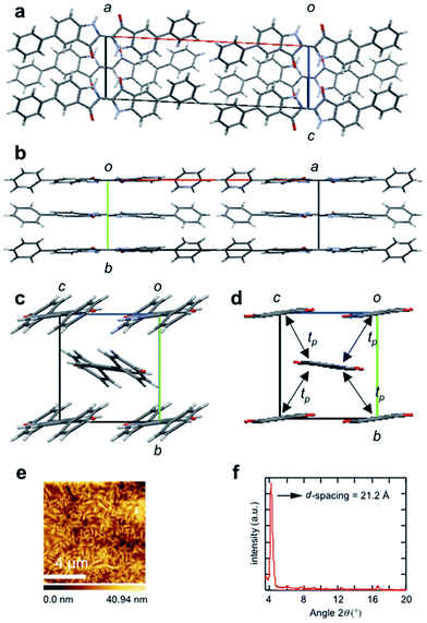 |
| | Fig. 5 Crystal structure of 2 viewed along the (a) b, (b) c, and (c and d) a axes. Hydrogen atoms and phenyl groups are omitted in (d). The transfer integral, tp, is estimated to be 20.4 meV for HOMO and 23.5 meV for LUMO. (e) AFM image of thin film of 2 (75 nm) deposited on a 20 nm film of TTC. (f) XRD pattern of 2. | |
From the molecular orbital calculation, the transfer integrals between the HOMOs as well as between the LUMOs are estimated as shown in the captions of Fig. 4 and 5. Charge carrier transport is confined in one dimension in 1, whereas two-dimensional carrier transport is expected in 2. The brickwork structure has been observed in cyclohexyl naphthalene diimide which attains high field-effect mobility.43 Although the present structure is different from the ideal brickwork structure, the network of the transfer integrals is identical to that of the cyclohexyl naphthalene diimide. It is noteworthy that the present characteristic molecular packing, which is a hybrid of the herringbone and brickwork structures, is induced by the steric effect of the two phenyl groups. The incorporation of the phenyl groups elongates the molecules to destroy the twisted stack structure. The whole molecules realize a herringbone structure, but interestingly the central parts realize an approximate brickwork structure. The remarkably enhanced mobility of 2 is mainly attributed to this brickwork packing that realizes two-dimensional transport, rather than the extended π-skeleton coming from the introduction of the phenyl groups.
Thin film properties
Atomic force microscopy (AFM) images of the thin films deposited on a TTC layer are shown in Fig. 4 and 5. The thin films of both 1 and 2 consist of highly crystalline domains due to the strong intermolecular π–π interactions together with the influence of the TTC passivation layers. It has been reported that the crystallinity of a wide variety of organic semiconductors increases when deposited on TTC, to achieve high mobility as well as ambipolar charge transport.14–16
As shown in Fig. 4d, a thin film of 1 shows X-ray diffraction (XRD) peaks at 2θ = 6.49° and 13.4°, corresponding to the d-spacing of 13.6 Å. This is almost equal to the length of the crystallographic a axis, implying that the a axis is perpendicular to the substrate. For 2, a sharp primary diffraction peak is observed at 2θ = 4.17°, corresponding to the d-spacing of 21.2 Å (Fig. 5f). This is again in good agreement with the crystallographic a axis, so that the molecules are standing perpendicular to the substrate. From the crystal structures, the molecular long axis of 1 is inclined by 36° from the normal to the substrate (Fig. 4b), while the molecules 2 are almost perpendicular to the substrate. It has been reported in naphthalene diimide series that the perpendicular orientation is most advantageous for charge transport in organic transistors.43 The tilt angle decreases in the order of 1 > 2 ∼ Tyrian purple > indigo, which is in complete agreement with the decreasing order of the mobility.
Transistor on an organic substrate
In order to explore a way to flexible devices, we have fabricated a transistor of 2 on an organic PEN substrate by using poly(3,4-ethylenedioxythiophene):poly(stylenesulfonate) (PEDOT:PSS) as a gate electrode, and a parylene C film as a gate dielectric (Fig. 6a). A pentacene transistor with the hole mobility of 0.3 cm2 V−1 s−1 has been reported using PEDOT:PSS as the gate contact.45,46 A pentacene ambipolar transistor in a bottom-gate top-contact geometry has been realized by using parylene C as the hydrophobic dielectric layer (μh/μe = 0.07–0.1/0.01–0.04 cm2 V−1 s−1), so parylene C is an inert enough material to achieve an ambipolar transistor.47 The XRD shows peaks at d = 21.2 Å and 6.33 Å (Fig. 6b), which respectively correspond to 2 and parylene C.48 As shown in Fig. 6d–f, the transistor shows well-balanced ambipolar characteristics, where the maximum hole and electron mobilities are 0.13 and 0.29 cm2 V−1 s−1, respectively. The AFM image (Fig. 6c) reveals decreased grain size, which may be related to the reduced transistor performance. The hole/electron threshold voltages extracted from the transfer characteristics are −25/120 V for VDS = 80 V and −50/90 V for VDS = −80 V, so the intrinsic threshold voltages are VTH = 120 V and V′TH = −50 V. These threshold voltages are proportional to the trap numbers at the semiconductor/dielectric interface. Although the threshold voltages are increased in comparison with the TTC transistors, parylene C is a promising gate dielectric material for an ambipolar transistor.
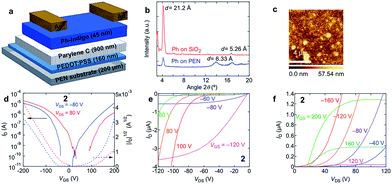 |
| | Fig. 6 (a) Structure of an indigo organic transistor on a PEN substrate in bottom-gate top-contact geometry, where L and W are 100 and 1000 μm, respectively. (b) XRD pattern of 2, (c) AFM image of a thin film of 2 (45 nm) deposited on a 900 nm film of parylene C film. (d) Transfer characteristics of a thin-film transistor of 2 on a PEN substrate. (e) Output characteristics at VDS < 0, and (f) at VDS > 0. | |
Conclusions
In summary, we have developed new indigo derivatives showing excellent ambipolar transistor properties. In particular, the transistor performance of 2 stems from the characteristic structure that is a hybrid of the herringbone and brickwork structures in contrast to the stacking structure of the parent indigo. Another important aspect is the well-balanced ambipolar properties achieved by a molecule with a minimal π-framework. Similarly, DPP in donor–acceptor polymers is not a simple acceptor as recognized generally, but DPP has ambipolar properties due to the electron-donating nitrogen atoms and the electron-withdrawing carbonyl groups.44 Although the operation of an ambipolar transistor is complicated depending on VGS and VDS, Fig. 1 clearly shows the relationships of the different operation modes. It should be emphasized that the unipolar region is large due to the large VTH – V′TH, and the reversed region is equivalently useful to the ordinary side. The present finding also suggests great possibilities of bio-inspired materials for the development of organic semiconductors.
Acknowledgements
The authors are grateful to Tokyo Institute of Technology Center for Advanced Materials Analysis for XRD measurement and Prof. Kakimoto for NMR and AFM measurements. This work was partly supported by a Grant-in Aid for Scientific Research (B) (no. 23350061) from the Ministry of Education, Culture, Sports, Science, and Technology of Japan.
Notes and references
- J. Zaumseil and H. Sirringhaus, Chem. Rev., 2007, 107, 1296 CrossRef CAS PubMed.
- S. Z. Bisri, C. Piliego, J. Gao and M. A. Loi, Adv. Mater., 2014, 26, 1176 CrossRef CAS PubMed.
- J. D. Yuen and F. Wudl, Energy Environ. Sci., 2013, 6, 392 CAS.
- Y. Zhao, Y. Guo and Y. Liu, Adv. Mater., 2013, 25, 5372 CrossRef CAS PubMed.
- Y. Olivier, D. Niedzialek, V. Lemaur, W. Pisula, K. Müllen, U. Koldemir, J. R. Reynolds, R. Lazzaroni, J. Cornil and D. Beljonne, Adv. Mater., 2014, 26, 2119 CrossRef CAS PubMed.
- E. Wang, W. Mammo and M. R. Andersson, Adv. Mater., 2014, 26, 1801 CrossRef CAS PubMed.
- J. D. Yuen, J. Fan, J. Seifter, B. Lim, R. Hufschmid, A. J. Heeger and F. Wudl, J. Am. Chem. Soc., 2011, 133, 20799 CrossRef CAS PubMed.
- Z. Chen, M. J. Lee, R. S. Ashraf, Y. Gu, S. Albert-Seifried, M. M. Nielsen, B. Schroeder, T. Anthopoulos, M. Heeney, I. McCulloch and H. Sirringhaus, Adv. Mater., 2012, 24, 647 CrossRef CAS PubMed.
- R. J. Chesterfield, C. R. Newman, T. M. Pappenfus, P. C. Ewbank, M. H. Haukaas, K. R. Mann, L. L. Miller and C. D. Frisbie, Adv. Mater., 2003, 15, 1278 CrossRef CAS.
- J. C. Ribierre, S. Watanabe, M. Matsumoto, T. Muto and T. Aoyama, Appl. Phys. Lett., 2010, 96, 083303 CrossRef PubMed.
- J. C. Ribierre, S. Ghosh, K. Takaishi, T. Muto and T. Aoyama, J. Phys. D: Appl. Phys., 2011, 44, 205102 CrossRef.
- A. Tapponnier, I. Biaggio and P. Günter, Appl. Phys. Lett., 2005, 86, 112114 CrossRef PubMed.
- T. D. Anthropoulos, C. Tanase, S. Setayesh, E. J. Meijer, J. C. Hummelen, P. W. M. Blom and D. M. de Leeuw, Adv. Mater., 2004, 16, 2174 CrossRef.
- M. Kraus, S. Richler, A. Opitz, W. Brütting, S. Haas, T. Hasegawa, A. Hinderhofer and F. Schreiber, J. Appl. Phys., 2010, 107, 094503 CrossRef PubMed.
- M. Kraus, S. Haug, W. Brütting and A. Opitz, Org. Electron., 2011, 12, 731 CrossRef CAS PubMed.
- A. Opitz, M. Horlet, M. Kiwull, J. Wagner, M. Kraus and W. Brütting, Org. Electron., 2012, 13, 1614 CrossRef CAS PubMed.
- J. Kan, Y. Chen, D. Qi, Y. Liu and J. Jiang, Adv. Mater., 2012, 24, 1755 CrossRef CAS PubMed.
- T. Sakanoue, M. Yahiro, C. Adachi, K. Takimiya and A. Toshimitsu, J. Appl. Phys., 2008, 103, 094509 CrossRef PubMed.
- E. C. P. Smits, T. D. Anthopoulos, S. Setayesh, E. von Veenendaal, R. Coehoorn, P. W. M. Blom, B. de Boer and D. M. de Leeuw, Phys. Rev. B: Condens. Matter Mater. Phys., 2006, 73, 205316 CrossRef.
- L.-Y. Chiu, H.-L. Cheng, H.-Y. Wang, W.-Y. Chou and F.-C. Tang, J. Mater. Chem. C, 2014, 2, 1823 RSC.
- J. H. Seo, G. S. Chang, R. G. Wilks, C. N. Whang, K. H. Chae, S. Cho, K.-H. Yoo and A. Moewes, J. Phys. Chem. B, 2008, 112, 16266 CrossRef CAS PubMed.
- F. Cicoira, N. Coppedé, S. Iannotta and R. Martel, Appl. Phys. Lett., 2011, 98, 183303 CrossRef PubMed.
- M. Irimia-Vlada, E. D. Głowacki, P. A. Troshin, G. Schwabegger, L. Leonat, D. K. Susarova, O. Krystal, M. Ullah, Y. Kanbur, M. A. Bodea, V. F. Razumov, H. Sitter, S. Bauer and N. S. Sariciftci, Adv. Mater., 2012, 24, 375 CrossRef PubMed.
- E. D. Głowacki, G. Voss and N. S. Sariciftci, Adv. Mater., 2013, 25, 6783 CrossRef PubMed.
- E. D. Głowacki, L. Lenonat, G. Voss, M. A. Bodea, Z. Buzkurt, A. M. Ramil, M. Irimia-Vlada, S. Bauer and N. S. Sariciftci, AIP Adv., 2011, 1, 042132 CrossRef PubMed.
- I. V. Klimovich, L. I. Leshanskaya, S. I. Troyanov, D. V. Anokhin, D. V. Novikov, A. A. Piryazev, D. A. Ivanov, N. N. Dremova and P. A. Troshin, J. Mater. Chem. C, 2014, 2, 7621 RSC.
- L. Serrano-Andrés and B. O. Roos, Chem.–Eur. J., 1997, 3, 717 CrossRef.
- S. Hotta and T. Yamao, J. Mater. Chem., 2011, 21, 1295 RSC.
- B. Noda, M. Katsuhara, I. Aoyagi, T. Mori, T. Taguchi, T. Kambayashi, K. Ishikawa and H. Takezoe, Chem. Lett., 2005, 34, 392 CrossRef CAS.
- P. W. Sadler, J. Org. Chem., 1955, 21, 316 CrossRef.
- S. Torii, T. Yamanaka and H. Tanaka, J. Org. Chem., 1978, 43, 2882 CrossRef CAS.
- E. Ziegler, H. G. Foraita and T. Kappe, Monatsh. Chem., 1967, 98, 324 CrossRef CAS.
- Y. Tanoue, A. Terada, K. Sakata, M. Hashimoto, S. Morishita, M. Hamada, N. Kai and T. Nagai, Fish. Sci., 2001, 67, 726 CrossRef CAS.
- Y. Tanoue, K. Sakata, M. Hashimoto, M. Hamada, N. Kai and T. Nagai, Dyes Pigm., 2004, 62, 101 CrossRef CAS.
- M. Prieto, E. Zurita, E. Rosa, L. Muñoz, P. Llod-Willams and E. Giralt, J. Org. Chem., 2004, 69, 6812 CrossRef CAS PubMed.
- M. L. Tang, A. D. Reichardt, P. Wei and Z. Bao, J. Am. Chem. Soc., 2009, 131, 5264 CrossRef CAS PubMed.
- H. von Eller, Bull. Soc. Chim. Fr., 1955, 1433 Search PubMed.
- H. von Eller, Bull. Soc. Chim. Fr., 1958, 316 Search PubMed.
- R. Süss and A. Wolf, Naturwissenschaften, 1980, 67, 2867 Search PubMed.
- R. Süss, M. Steins and V. Kupcik, Z. Kristallogr., 1988, 184, 269 CrossRef PubMed.
- F. Kettner, L. Hüter, J. Schäfer, K. Röder, U. Purgahn and H. Krautscheid, Acta Crystallogr., Sect. E: Struct. Rep. Online, 2011, 67, 2867 Search PubMed.
- S. Larsen and F. Watjen, Acta Chem. Scand., Ser. A, 1980, 34, 171 CrossRef PubMed.
- T. Kakinuma, H. Kojima, M. Ashizawa, H. Matsumoto and T. Mori, J. Mater. Chem. C, 2013, 1, 5395 RSC.
- H. Kojima and T. Mori, Chem. Lett., 2013, 42, 68 CrossRef CAS.
- M. Halik, H. Klauk, U. Zschieschang, G. Schmid, W. Radlik and W. Weber, Adv. Mater., 2002, 14, 1717 CrossRef CAS.
- Y. Jang, Y. D. Park, J. A. Lim, H. S. Lee, W. H. Lee and K. Cho, Appl. Phys. Lett., 2006, 89, 183501 CrossRef PubMed.
- S. R. Saudari, Y. J. Lin, Y. Lai and C. R. Kagan, Adv. Mater., 2010, 22, 5063 CrossRef CAS PubMed.
- J. Jakabovič, J. Kováč, M. Weis, D. Haško, R. Srnánek, P. Valent and R. Resel, Microelectron. J., 2009, 40, 595 CrossRef PubMed.
Footnote |
| † Electronic supplementary information (ESI) available: Additional information on synthesis, thermal analysis, redox properties, UV-vis spectra, gradual channel approximation, single crystal structures, theoretical calculations, device fabrication, and device air stability. CCDC 1002555 and 1002556. For ESI and crystallographic data in CIF or other electronic format see DOI: 10.1039/c4tc01563k |
|
| This journal is © The Royal Society of Chemistry 2014 |
Click here to see how this site uses Cookies. View our privacy policy here. 
 Open Access Article
 This Open Access Article is licensed under a