
Ideal two-dimensional systems with a gain Rashba-type spin splitting: SrFBiS2 and BiOBiS2 nanosheets
Yandong
Ma
,
Ying
Dai
*,
Na
Yin
,
Tao
Jing
and
Baibiao
Huang
School of Physics, State Key Laboratory of Crystal Materials, Shandong University, Jinan 250100, People's Republic of China. E-mail: daiy60@sina.com
First published on 18th August 2014
Abstract
The Rashba effect is increasingly seen as the key ingredient in the burgeoning field of spintronics. However, the lack of two-dimensional materials with a large Rashba effect hinders its practical applications. Here, with density functional theory, we report giant Rashba-type spin splitting in SrFBiS2 and BiOBiS2 nanosheets originating from their hidden local polar atomic configurations. Owing to the weak interactions between the two BiS2 layers, they hold two individual Rashba spin splittings belonging to two opposite BiS2 layers, which are degenerated because of their inversion symmetry. As a result, with small perturbations, such as a tiny electric field, we observe two sets of Rashba spin splittings in both materials; this is different from most of the previous studied Rashba systems, in which there is only one set of Rashba spin splitting. More interestingly, the strength of the Rashba effect in both nanosheets can be preserved while their bandgap can be effectively tuned by applying an external electric field.
I. Introduction
The spin–orbit interaction (SOI), which is a relativistic effect in electron system, tends to lift the degeneracy of energy bands. In systems with inversion (I) symmetry, such splitting leaves the energy states spin-degenerate, as long as the time reversal (T) symmetry is held.1–5T-symmetry connects the states ϕK,↑ and ϕK,−↑, whereas I-symmetry enforces the degeneracy between ϕK,↑(↓) and ϕ−K,↑(↓). Breaking I-symmetry lifts the latter constraint, and allows the energy bands to be spin-split at generic k-points.1,5 In this environment, two electrons with the same energy, but with different spins will have different magnitudes of the wave vector, which generates different phase shifts during transport.6 This spin-dependent phase shift is of key relevance for technological applications in spin transistors and spintronics.7 Rashba spin splitting (RSS)8 exemplifies this situation, as described by HR = p2/2m + ν[e(s × p)], where e is the direction of the potential gradient, breaking I-symmetry, and s and p are the spin and momentum operators, respectively. The resulting energy dispersion relations of the free electrons split from the spin-degenerate parabolic bands can be denoted by E±(![[k with combining right harpoon above (vector)]](https://www.rsc.org/images/entities/i_char_006b_20d1.gif) ) = ℏ22/2m* ± αR||, where m* represents the effective mass of the electron. Here, αR is called the Rashba parameter and represents the strength of Rashba spin-splitting. This effect has been demonstrated in wurtzite semiconductors,9,10 such as CdS and CdSe, and more importantly it is appealing for application in semiconductor heterostructures.11 Subsequently, spin-polarized states were experimentally observed by spin-resolved angular-resolved photoemission spectroscopy (SRARPES) when looking at the surface states of nonmagnetic metals with large atomic spin–orbit coupling, such as Au (111)12 and Bi (111).13 Furthermore, the discovery of giant Rashba-type splitting realized at noble-metal-based surface alloys14 has been attracting considerable interest, where heavy elements with a strong atomic SOI are incorporated into the surface. A recent study was extended to bulk materials, i.e., a giant bulk Rashba effect was discovered in the polar semiconductor BiTeI,4 even though its typical layered crystalline structure makes it closer to a 2D system, or to a system with a preferential direction. In addition, large spin splitting in the ferroelectric narrow-gap semiconductor GeTe was also predicated, which is characterized by the relatively small spin–orbit interaction.15 The realization of such electron systems with high-energy-scale Rashba splitting will provide opportunities for practical spintronic applications,16 as well as hosting non-trivial phenomena such as the intrinsic spin Hall effect17 and non-centrosymmetric exotic superconductivity.18
) = ℏ22/2m* ± αR||, where m* represents the effective mass of the electron. Here, αR is called the Rashba parameter and represents the strength of Rashba spin-splitting. This effect has been demonstrated in wurtzite semiconductors,9,10 such as CdS and CdSe, and more importantly it is appealing for application in semiconductor heterostructures.11 Subsequently, spin-polarized states were experimentally observed by spin-resolved angular-resolved photoemission spectroscopy (SRARPES) when looking at the surface states of nonmagnetic metals with large atomic spin–orbit coupling, such as Au (111)12 and Bi (111).13 Furthermore, the discovery of giant Rashba-type splitting realized at noble-metal-based surface alloys14 has been attracting considerable interest, where heavy elements with a strong atomic SOI are incorporated into the surface. A recent study was extended to bulk materials, i.e., a giant bulk Rashba effect was discovered in the polar semiconductor BiTeI,4 even though its typical layered crystalline structure makes it closer to a 2D system, or to a system with a preferential direction. In addition, large spin splitting in the ferroelectric narrow-gap semiconductor GeTe was also predicated, which is characterized by the relatively small spin–orbit interaction.15 The realization of such electron systems with high-energy-scale Rashba splitting will provide opportunities for practical spintronic applications,16 as well as hosting non-trivial phenomena such as the intrinsic spin Hall effect17 and non-centrosymmetric exotic superconductivity.18
Although most Rashba systems exist in surfaces and bulk materials, two-dimensional (2D) ultrathin nanosheets with a strong SOI have obvious merit in manipulating the spin carriers. Recently, as rapidly emerging, two-dimensional materials have provided new opportunities to satisfy the people's requirements of ultrathinness, transparency and flexibility in high-level integrated electronic systems, in which two-dimensionality could provide a bridge to combine microscopic compressibility (for integration) with macroscopic extensibility (for operation), guaranteeing the maximum functionality while keeping the size minimized. Moreover, Rashba spin splitting is a 2D relativistic effect. However, to date, the 2D systems, such as graphene and silicene, exhibit only small spin splitting (10−3 and 1 meV for graphene and silicene, respectively),19,20 which is far from the requirement for practical applications. For 2D materials with heavy atoms, the magnitude of the SOI effect is also not large enough.21 More recently, a substantial Rashba effect was observed for some 2D systems,22,23 such as graphene in contact with Au. However, with all the existing developments, a little attention has paid to obtain 2D nanosheets with large Rashba spin splitting for novel spintronic applications.
In this work, we report the identification of two novel 2D nanosheets with a giant Rashba effect SrFBiS2 and BiOBiS2 derived from their particular local polar atomic configurations using relativistic calculations within density functional theory. We find that in SrFBiS2 (BiOBiS2) nanosheets can be described in terms of an ionic-like model, where the covalent coupling of Sr and F (Bi and O) atoms forms positive (Sr2F2)2+ [(Bi2O2)2+] layers, whereas the covalent coupling of Bi and S atoms forms negative (BiS2)− layers; hence, the Sr2F2–BiS2 (Bi2O2–BiS2) interaction could be considered as ionic. Thus, the crystal structure possesses two ionic-like strong polar fields along the stacking direction, from the Sr2F2 to BiS2 layers and Bi2O2 to BiS2 layers for the SrFBiS2 and BiOBiS2 nanosheets, respectively. In both the materials, we found that they hold two remarkable counter-helical Rashba spin splitting from opposite nanosheet surfaces, which are degenerated as a result of the strong inversion symmetry. Owing to their peculiar structure, different from most previously studied Rashba systems, we could obtain two sets of Rashba spin splitting with a small perturbation, such as a tiny electric field. More interestingly, the strength of the Rashba effect in both 2D nanosheets can be almost preserved, while their bandgap can be effectively tuned by applying electric field. Together with their ultrathin thickness (down to 1 nm, considerably thinner than most Rashba materials with comparable strength), the giant-Rashba 2D nanosheets, SrFBiS2 and BiOBiS2, possess excellent potential for applications to various spin-dependent electronic functions.
II. Computational methods
The structural and electronic characteristics of SrFBiS2 and BiOBiS2 nanosheets using DFT are performed using the plane wave basis Vienna ab initio simulation pack (VASP) code.24,25 In first principles calculations, the ion-electron interactions are treated with the projected augmented wave (PAW) approximation.26,27 The exchange–correlation potentials are treated with the generalized gradient approximation parameterized by Perdew–Burke–Ernzerhof (PBE).28 The wave functions are expanded in plane waves up to 450 eV and the convergence threshold for energy is 10−4 eV. The Brillouin zone integration is carried out at 9 × 9 × 1 and 15 × 15 × 1 Monkhorst–Pack29k-grids, respectively, for geometry optimization and self-consistent electronic structure calculation, and 200 uniform k-points along the 1D Brillouin zone are used to obtain the band structure. The cell parameters and the atomic coordinates of the nanosheets are fully relaxed until the force acting on every atom is less than 0.02 eV Å−1. The periodic boundary condition is set with the vacuum region between two neighboring ribbons larger than 18 Å. The spin–orbit coupling effect, which is important for the heavy elements considered here, is treated self-consistently in fully relativistic pseudopotentials for the valence electrons.30We wish to point out that although the PBE method usually underestimates the band gap of semiconductors, an accurate energy gap may be evaluated using more sophisticated HSE or GW methods. However, the results on the occupied states, the dispersion of the band, the characters of the band structures, as well as the relative variation calculated by PBE are expected to be qualitatively reasonable and reliable, which has been employed by previous theoretical studies4,6,31,32 on the Rashba effect. For convenient comparison, all the calculations in the present work were also performed using the same method as that in previous studies.
III. Results and discussion
Layered materials are defined as solids with strong in-plane chemical bonds, but weak out-of plane van der Waals bonds. Such materials can be sheared parallel or expanded normal to the in-plane direction. In the extreme limit, these processes yield nanometer-thin, even atomically thin, sheets that are not characteristic of the bulk precursor. This production of extremely thin sheets from layered precursors is known as exfoliation or delamination. The sheets produced are generally referred to as nanosheets, where “nano” refers to the magnitude of the thickness. SrFBiS2 and BiOBiS2 are two new layered compounds recently discovered to be crystallized in a tetragonal structure in the space group, P4/nmm.33,34 The representative unit cells of SrFBiS2 and BiOBiS2 are shown in Fig. 1. Despite the composing difference, both compounds have analogous structures to ZrCuSiAs and have semiconducting behavior with a relatively small bandgap. Similar to ZrCuSiAs, SrFBiS2 (BiOBiS2) is built up by stacking up SrF (BiO) layers and NaCl-type BiS2 layers alternatively along the c axis. Within each monolayer, the Sr2F2–BiS2 (Bi2O2–BiS2) interactions could be considered as ionic. One BiS2 layer contains one BiS plane (namely the Bi-S1 plane) and one pure S planes (i.e., the S2 plane), as illustrated in Fig. 1. Consistent with layered materials, for both the materials, although the bonding within each monolayer is strong, the adjacent BiS2 layers are held together by weak van der Waals interactions. In this regard, similar to the case in graphite, the weak coupling between the adjacent BiS2 layers makes it possible for the bulk materials to exfoliate to atomic thin sheets using mechanical exfoliation, as reported in ref. 35. In fact, to date, a range of layered compounds have been synthesized as nanosheets.36–39 The archetypal example is graphite, which consists of stacked graphene monolayers. There are many other examples from VS2 and layered clays to more exotic examples, such as MoO3, GaTe and Bi2Se3.39 Hence, it is relatively easy for 2D SrFBiS2 and BiOBiS2 structures to be exfoliated from the parent 3D layered SrFBiS2 and BiOBiS2. | ||
| Fig. 1 Crystal structure of (a and b) SrFBiS2 and (c and d) BiOBiS2. The corresponding unit cells are presented as red rectangles. Red, green, blue, gray, and orange balls denote Bi, S, Sr, F, and O atoms, respectively. | ||
From a structural point of view, a single layer structure of SrFBiS2 (BiOBiS2) can be viewed as a three-layer stacking of SrF (BiO) and BiS2, wherein a SrF (BiO) layer is sandwiched between the layers of NaCl-type BiS2. After geometry optimization, the SrFBiS2 nanosheets can be described by the plane group P4/nmm with a lattice constant of 4.041 Å and a thickness down to 11.131 Å containing ten atoms in each cell. The BiOBiS2 nanosheets of the plane group P4/nmm has a lattice constant of 3.959 Å and an equivalent thickness of about 11.317 Å, also contains ten atoms in each cell. The cohesive energies relative to free constituent atoms are calculated to understand their stability. The cohesive energy per atom is calculated using the expression, 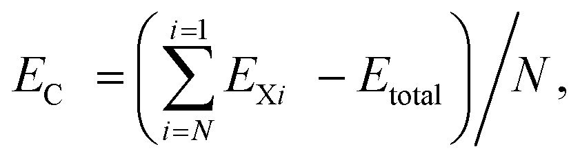 in terms of the total energy of SrFBiS2 or BiOBiS2 nanosheets (Etotal), the total energies of free constituent atoms (Exi) and the total number of the atoms in the cell (N). We find that the calculated cohesive energies are all positive and in the range of 4–5 eV, indicating a strong cohesion relative to the free atoms of the constituents. This value is comparable to most of the MX2 (M, transition metal; X, chalcogen atom) monolayers; the cohesive energies per atom of most MX2 monolayers are in the range of 3–7 eV.40 Although a comparable value of EC alone is not sufficient to indicate whether a given nanosheet structure can form, the binding energy, Eb, to its bulk phase is usually taken to be a good criterion to check the stability of the nanosheets exploited from the layered bulk phase. Because the layered bulk compound is stable, if the binding energy is small, the exfoliated nanosheet could be stable. The binding energy, Eb, is obtained by subtracting the total energies of the constituent triple layer, Esheet, from the total energies of the corresponding bulk phases, Ebulk Specifically, Eb = (Ebulk − Esheet)/N. The calculated binding energy for SrFBiS2 and BiOBiS2 is only −17 and −12 meV. On the other hand, for most of the MX2 monolayers, the binding energy is significantly lower than the cases of SrFBiS2 and BiOBiS2; for example, the counterpart of MoS2 is −73 meV.41 This indicates that compared to layered MoS2, the van der Waals interactions between SrFBiS2 or BiOBiS2 nanosheets are even weaker. Given the present analysis, SrFBiS2 and BiOBiS2 can be readily exfoliated into stable nanosheets. Details of exfoliation strategies are summarized in ref. 39.
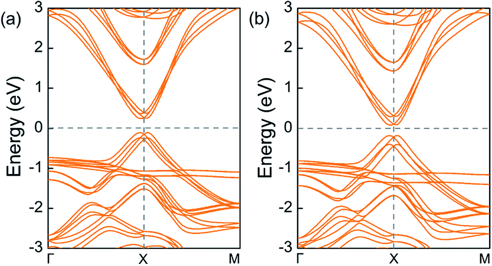
Fig. 2 depicts the respective band structures for both the systems. In the absence of SOI, they show semiconducting behavior with a direct energy gap of 0.89 and 1.00 eV for SrFBiS2 and BiOBiS2 nanosheets, respectively. As shown in Fig. 2, the smallest bandgap is found to be between the bands α and β at the X point of the Brillouin zone. We find that the valence and conduction bands near the Fermi level of both the materials is mainly located on the BiS2 layers, while the SrF and BiO layers make little contribution, which can be omitted. In that case, the SrF and BiO layers in SrFBiS2 and BiOBiS2 nanosheets, respectively, can be regarded as a potential barrier thwarting the wave function overlap of the opposite BiS2 layers. Based on this discussion, together with the fact that bands α and β are derived from BiS2 layers, they should be two-fold degenerate without considering the spin. A further examination of the bands indicates that for the k-point along the X–M direction, the bands α and β are nearly two-fold degenerate bands. While for the k-point along the X–Γ direction, the bands α and β are two-fold degenerate bands. Evidently, the band structures from the two surfaces are significantly analogous.
 | ||
| Fig. 2 Electronic structure of (a and b) SrFBiS2 and (c and d) BiOBiS2 nanosheets with and without SOI. The Fermi energy is set to 0 eV. | ||
Turning on SOI, the band structures of both the materials undergo a drastic change. As shown in Fig. 2, the bandgap of SrFBiS2 and BiOBiS2 nanosheets is closed to 0.48 and 0.50 eV, respectively, which are nearly one time smaller than that obtained without SOI [as shown in Fig. 2(a) and (c)]. This is mainly because of the strong SOI of the constituent atoms in both the materials. Note that, the valence and conduction bands near the Fermi level of both the materials are mainly located on the BiS2 layers, indicating that all the bands near the Fermi level are essentially p-type. Under the crystal field, the p states would split because of the negative crystal-field splitting of the VBM and positive crystal-field splitting of CBM. Without SOI, the VBM and CBM both become pz type. For the convenience of our discussion, we refer to them as pvz and pcz, respectively. By introducing SOI, both the spin and orbital mixing are allowed. Consequently, pvz and pcx split again into the corresponding states of  and
and  . This effect thereby reduces the bandgap of SrFBiS2 (BiOBiS2) nanosheets from 0.89 (1.00) eV to 0.48 (0.50) eV.
By looking at the band dispersions near the Fermi level of the SrFBiS2 and BiOBiS2 nanosheets in the presence of SOI, the conduction band minimum (CBM) and valence band maximum (VBM), which disperse from the X-point toward the zone boundaries, are spin split and are located away from the X-point, see Fig. 2(b) and (d). This result strongly suggests that a typical Rashba effect in SrFBiS2 and BiOBiS2 nanosheets. That is, Rashba spin splitting occurs not only to an electron at CBM, but also to a hole at VBM. In the standard Rashba–Bychkov model for a two-dimensional electron gas,42 the strength of Rashba splitting is characterized by three parameters: the momentum offset (k0), the Rashba energy (ER), and the Rashba coupling constant (αR). They are related by ER = ℏ2k02/2m* and k0 = m*αR/ℏ2. When k0 and ER are determined, αR can be readily evaluated. The results obtained for SrFBiS2 and BiOBiS2 nanosheets, as listed in Table 1, are considerably larger than the typical values for Rashba splitting in conventional semiconductor quantum wells.11,43 They are comparable to systems with enhanced Rashba splitting.44,45 For example, these results for VBM along the X–M directions show that (k0, ER, αR) = (0.029 Å−1, 36.1 meV, 2.53 eV Å) and (k0, ER, αR) = (0.018 Å−1, 18.1 meV, 2.06 eV Å) for SrFBiS2 and BiOBiS2 nanosheets, respectively. Table 1 also indicates that slight anisotropic Rashba spin splitting emerges in both the materials. More importantly, different from most of the previous materials with a comparable effect, one distinct advantage of both the materials here is their two-dimensional configurations, which can provide opportunities to satisfy people's requirements of ultrathinness and flexibility in high-level integrated electronic systems. Overall, SrFBiS2 and BiOBiS2 nanosheets will have important roles in spintronic applications, as they guarantee a large Rahsba effect, while keeping the size at a minimum, down to 1 nm.
| VBM | CBM | ||||||
|---|---|---|---|---|---|---|---|
| k 0 | E R | α R | k 0 | E R | α R | ||
| SrFBiS2 | X–Γ | 0.034 | 39.8 | 2.30 | 0.026 | 23.2 | 1.79 |
| X–M | 0.029 | 36.1 | 2.53 | 0.018 | 17.1 | 1.89 | |
| BiOBiS2 | X–Γ | 0.023 | 14.7 | 1.25 | 0.011 | 3.8 | 0.68 |
| X–M | 0.018 | 18.1 | 2.06 | 0.008 | 2.8 | 0.70 | |
As mentioned above, SrFBiS2 (BiOBiS2) nanosheets have a triple-layer structure with a SrF (BiO) layer sandwiched between two BiS2 layers, suggesting that both the materials are centrosymmetric systems. We note that the strength of the Rashba effect is associated with, besides a strong atomic spin–orbit coupling atomic contribution, a potential gradient. In other words, the Rashba effect requires the breaking of inversion symmetry. At this point, because the condition is not satisfied in SrFBiS2 and BiOBiS2 nanosheets, the spin degeneracy in both the materials was supposed to be preserved upon the introduction of SOI, making them no-Rashba-type systems. Yet, we find that this is not the case. In contrast, Rashba spin splitting indeed occurs not only to an electron at CBM, but also to a hole at the VBM for both the materials. In fact, this discrepancy can be easily understood by looking at the special atomic configurations of the SrFBiS2 and BiOBiS2 nanosheets. In detail, structural analysis indicates that the structures of the SrFBiS2 (BiOBiS2) nanosheets can be described in terms of a ionic-like model, where the covalent coupling of Sr (Bi) and F (O) atoms forms positive (Sr2F2)2+ [(Bi2O2)2+] layers, whereas the covalent coupling of Bi (Bi) and S (S) atoms forms negative (BiS2)− [(BiS2)−] layers; hence, the Sr2F2–BiS2 (Bi2O2–BiS2) contacts could be considered as ionic. Because of this intriguing configuration, the crystal structure possesses two ionic-like strong local dipole moments along the stacking direction with opposite directions, from the Sr2F2 to BiS2 layers and Bi2O2 to two BiS2 layers for the SrFBiS2 and BiOBiS2 nanosheets, respectively. Because the local dipole moments are shifted in opposite directions, a vector sum of the dipole moments results in a net dipole moment of zero. However, in SrFBiS2 (BiOBiS2) nanosheets, the SrF (BiO) layer acts as a blocking barrier, although the thickness of both the materials is only 1 nm. Therefore, the wave function of the opposite BiS2 layers has little interaction with each other, indicating that the local dipole moment from one BiS2 layers could not be affected by that of the other BiS2 layers. These two individual dipole moments behave like two local structural inversion symmetry. To be more specific, the BiS2 layers can be regarded as two individual Rashba systems. With these analyses, the reason for large Rashba spin splitting in SrFBiS2 and BiOBiS2 nanosheets can be easily understood, although they are global inversion symmetric. In both materials, they hold two remarkable counter-helical Rashba spin splittings from opposite nanosheet surfaces, which are degenerated as a result of the global inversion symmetry. Because of their peculiar structure, different from most of the previously studied Rashba systems, we could obtain two Rashba spin splittings with a small perturbation, such as a tiny electric field.
To elucidate the two sets of Rashba spin splittings in more detail, we applied an external electric field (E-field) perpendicular to the nanosheet plane. Taking SrFBiS2 nanosheets as an example, we applied an external electric field to study the dependence of the electric and spintronic character on the external electric field. Because of the lattice symmetry, only one direction of the E-field perpendicular to the planes of SrFBiS2 nanosheets is considered. Here, we define the positive direction of the E-field as pointing along the +z direction. In Fig. 3a, we present the band structures of the SrFBiS2 nanosheets under E-field = 0.05 V Å−1. Remarkably, the degenerate Rashba bands are split and significantly separated from each other under an external electric field. This confirms that there are indeed two individual Rashba systems, or in other words, two individual Rashba spin splittings in the SrFBiS2 nanosheets, which originate from the slight coupling between the BiS2 layers. Such separation is caused by the potential difference between the two opposite BiS2 layers provoked by the electric field. This indicates that the two degenerate and individual spin states belonging to the top and bottom BiS2 layers are separated not only spatially, but also energetically. This demonstrates that two sets of Rashba spin splittings in one system appear simultaneously, which is different from most of the previously studied Rashba systems. More interestingly, by enhancing the E-field, the potential difference between the two opposite BiS2 layers increases in energy, yielding an enhanced separation of the degenerate Rashba bands. On the other hand, with increasing E-field, the band gap of the SrFBiS2 nanosheets rapidly decreases, see Fig. 4a. As a result, the band gap of the SrFBiS2 nanosheets close to 53 meV is established, see the SrFBiS2 nanosheets with E-field = 0.2 V Å−1 in Fig. 4a, as an example. Such promising bandgap modulation in the SrFBiS2 nanosheets arises from the Stark effect, which has been estimated in previous systems.22,46 In detail, under an external E-field, the electrostatic energy difference between the top and bottom BiS2 layers is provoked. This makes the bands in the top and bottom BiS2 layers shift in opposite directions. Therefore, the highest occupied orbital level and the lowest unoccupied orbital level of the SrFBiS2 nanosheets obtain from different BiS2 layers. Consequently, moving of energy bands in opposite directions results in a decrease in bandgap. One important question should be clarified, whether—and to what extent—the strength of the Rashba effect in the SrFBiS2 nanosheets can be tuned by adjusting the external E-field. This topic is of fundamental relevance because the large Rashba effect is highly desirable for enhancing the coupling between electron spins and the electricity relevant for spintronic functions. To clarify this concern, we investigated the effect of an E-field on the above three quantities. From the corresponding results displayed in Fig. 4, one can see that, in contrast to the significant variation of the bandgap, the Rashba parameters remain almost the same as the case without an E-field. An explanation of this interesting feature is sought in its peculiar atomic configuration. In the SrFBiS2 nanosheets, the Sr2F2–BiS2 bonding is ionic. Owing to this intriguing configuration, the crystal structure possesses two strong intrinsic E-fields with opposite directions, even when no external E-field is applied. Namely, compared to the giant intrinsic E-field, the applied external E-field is negligible. Bearing in mind that the Rashba spin splitting in the SrFBiS2 nanosheets derives from the giant intrinsic E-field, one can readily understand why the external E-field cannot significantly affect the Rashba effect, although the bandgap can be effectively tuned by the external E-field. The robust Rashba spin splitting in response to an external electric field in these novel nanosheets, together with their ultrathin thickness down to 1 nm, will greatly broaden the scientific impact of Rashba systems in spintronic applications.
 | ||
| Fig. 3 Electronic structure of SrFBiS2 nanosheets under (a) E-field = 0.05 V Å−1 and (b) E-field = 0.1 V Å−1. The Fermi energy was set to 0 eV. | ||
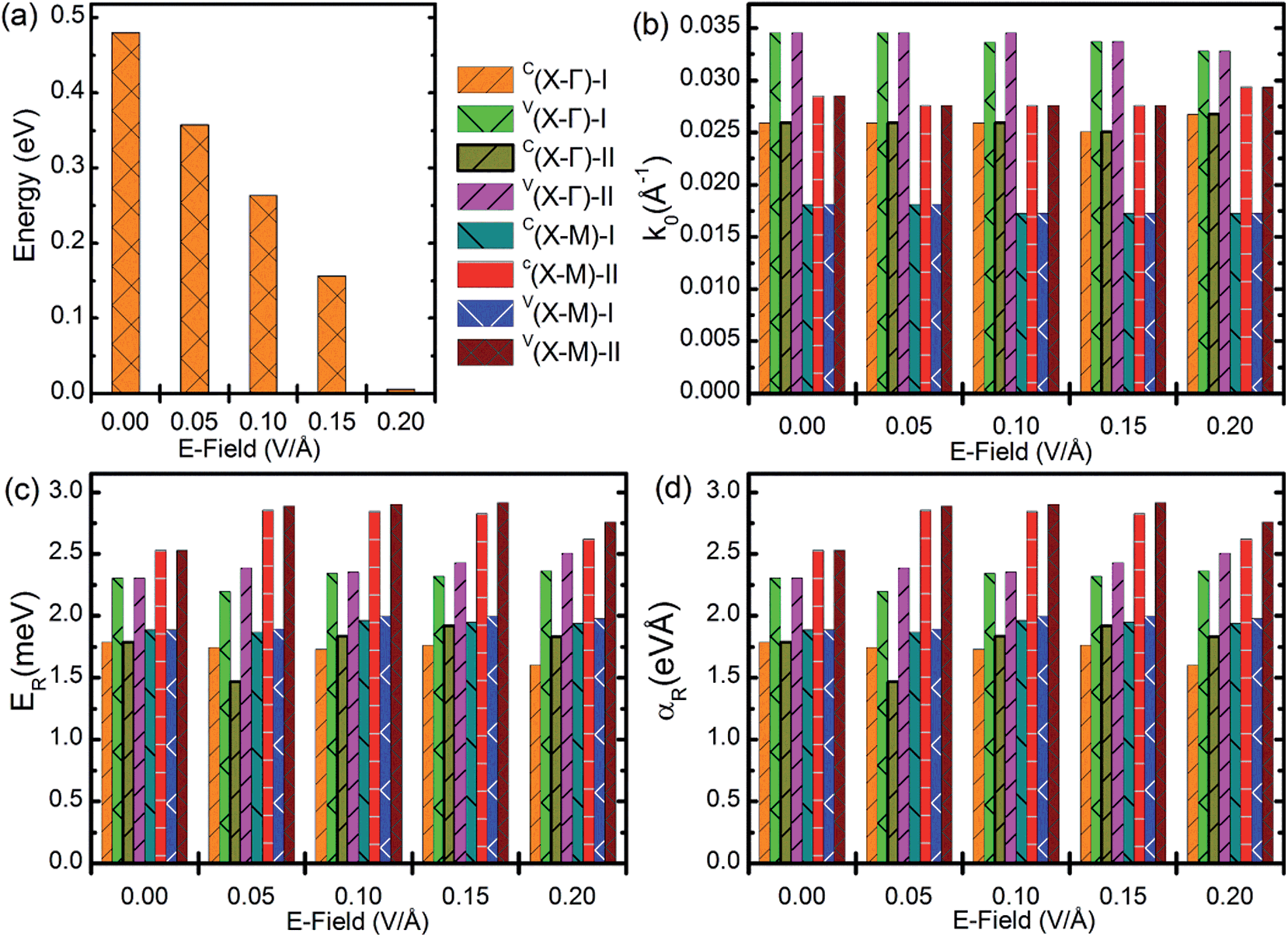 | ||
| Fig. 4 (a) Energy gap of SrFBiS2 nanosheets with SOI under different E-field conditions. (b) Momentum offset k0 of SrFBiS2 nanosheets under different E-field conditions. (c) Rashba energy ER of SrFBiS2 nanosheets under different E-field conditions. (d) Rashba parameterαR of SrFBiS2 nanosheets with SOI under different E-field conditions. I and II correspond to two sets of Rashba spin splittings, respectively. | ||
Finally, it should be noted that materials with analogous structures, but with compositional differences to SrFBiS2 and BiOBiS2 may show similar Rashba-type spin splitting.
IV. Summary
In conclusion, using first-principles calculations, we presented the findings of a huge spin–orbit interaction effect in two novel 2D nanosheets, SrFBiS2 and BiOBiS2, where the carriers not only at CBM, but also at VBM are ruled by large Rashba-like spin splitting. In the SrFBiS2 (BiOBiS2) nanosheets, there are two strong polar fields from the SrF (BiO) layer to the BiS2 layers. Although the thickness of both the materials is only 1 nm, the SrF (BiO) layer acts as a blocking barrier. Therefore, the local dipole moment from one BiS2 layers could not be affected by that of the other BiS2 layers, indicating that the two BiS2 layers can be regarded as two individual Rashba systems. Therefore, both the materials hold two remarkable Rashba spin splittings corresponding to two top and bottom BiS2 layers, which are degenerated as a result of the strong inversion symmetry. Upon applying an external E-field, the two degenerate and individual spin states belonging to the top and bottom BiS2 layers are separated not only spatially, but also energetically, thus we could obtain two sets of the Rashba spin splittings in a single system. More interestingly, although a reasonable external E-field can effectively tune the bandgap of SrFBiS2 and BiOBiS2 nanosheets, it cannot change the Rashba spin splitting significantly. This is because intrinsic polar field is so large that a reasonable external E-field cannot enhance or diminish the polar field related to the Rashba splitting. These findings make them promising platforms for the Rashba effect.Acknowledgements
This work is supported by the National Basic Research Program of China (973 program, 2013CB632401), National Science foundation of China under Grant 21333006, 11174180, and the Fund for Doctoral Program of National Education 20120131110066, the Natural Science Foundation of Shandong Province under Grant number ZR2011AM009, and the National Natural Science Foundation of China (Grant no. 51102153).Notes and references
- Y. Kato, R. C. Myers, A. C. Gossard and D. D. Awschalom, Nature, 2004, 427, 50 CrossRef CAS PubMed.
- M. S. Bahramy, R. Arita and N. Nagaosa, Phys. Rev. B: Condens. Matter Mater. Phys., 2011, 84, 041202 CrossRef.
- G. A. H. Schober, H. Murakawa, M. S. Bahramy, R. Arita, Y. Kaneko, Y. Tokura and N. Nagaosa, Phys. Rev. Lett., 2007, 108, 247208 CrossRef.
- K. Ishizaka, M. S. Bahramy, H. Murakawa, M. Sakano, T. Shimojima, T. Sonobe, K. Koizumi, S. Shin, H. Miyahara, A. Kimura, K. Miyamoto, T. Okuda, H. Namatame, M. Taniguchi, R. Arita, N. Nagaosa, K. Kobayashi, Y. Murakami, R. Kumai, Y. Kaneko, Y. Onose and Y. Tokura, Nat. Mater., 2011, 10, 521 CrossRef CAS PubMed.
- M. S. Bahramy, B.-J. Yang, R. Arita and N. Nagaosa, Nat. Commun., 2012, 3, 679 CrossRef CAS PubMed.
- H. X. Fu, Phys. Rev. B: Condens. Matter Mater. Phys., 2013, 87, 075139 CrossRef.
- S. Datta and B. Das, Appl. Phys. Lett., 1990, 56, 665 CrossRef CAS PubMed.
- E. I. Rashba, Phys. Solid State, 1960, 2, 1109 Search PubMed.
- Y. A. Bychkov and E. I. Rashba, JETP Lett., 1984, 39, 78 Search PubMed.
- R. C. Casella, Phys. Rev. Lett., 1960, 5, 371 CrossRef.
- J. Nitta, T. Akazaki, H. Takayanagi and T. Enoki, Phys. Rev. Lett., 1997, 78, 1335 CrossRef CAS.
- S. LaShell, B. A. McDougall and E. Jensen, Phys. Rev. Lett., 1996, 77, 3419 CrossRef CAS.
- Y. M. Koroteev, G. Bihlmayer, J. E. Gayone, E. V. Chulkov, S. Blügel, P. M. Echenique and P. Hofmann, Phys. Rev. Lett., 2004, 93, 046403 CrossRef.
- C. R. Ast, J. Henk, A. Ernst, L. Moreschini, M. C. Falub, D. Pacilé, P. Bruno, K. Kern and M. Grioni, Phys. Rev. Lett., 2007, 98, 186807 CrossRef.
- D. D. Sante, P. Barone, R. Bertacco and S. Picozzi, Adv. Mater., 2013, 25, 509 CrossRef PubMed.
- S. Datta and B. Das, Appl. Phys. Lett., 1990, 56, 665 CrossRef CAS PubMed.
- J. Sinova, d. Culcer, Q. Niu, N. A. Sinitsyn, T. Jungwirth and A. H. MacDonald, Phys. Rev. Lett., 2004, 92, 126603 CrossRef.
- E. Bauer, G. Hilscher, H. Michor, C. Paul, E. W. Scheidt, A. Gribanov, Y. Seropegin, H. Noël, M. Sigrist and P. Rogl, Phys. Rev. Lett., 2004, 92, 027003 CrossRef CAS.
- H. Min, J. E. Hill, N. A. Sinitsyn, B. R. Sahu, L. Kleinman and A. H. MacDonald, Phys. Rev. B: Condens. Matter Mater. Phys., 2006, 74, 165310 CrossRef.
- C.-C. Liu, W. Feng and Y. Yao, Phys. Rev. Lett., 2011, 107, 076802 CrossRef.
- H. Zeng, J. Dai, W. Yao, D. Xiao and X. Cui, Nat. Nanotechnol., 2012, 7, 490 CrossRef CAS PubMed.
- Q. H. Liu, Y. Z. Guo and A. J. Freeman, Nano Lett., 2013, 13, 5264 CrossRef CAS PubMed.
- D. Marchenko, A. Varykhalov, M. R. Scholz, G. Bihlmayer, E. I. Rashba, A. Rybkin, A. M. Shikin and O. Rader, Nat. Commun., 2012, 3, 1232 CrossRef CAS PubMed.
- G. Kresse and J. Furthmüller, Comput. Mater. Sci., 1996, 6, 15 CrossRef CAS.
- G. Kresse and J. Furthmüller, Phys. Rev. B: Condens. Matter Mater. Phys., 1996, 54, 11169 CrossRef CAS.
- P. E. Blöchl, Phys. Rev. B: Condens. Matter Mater. Phys., 1994, 50, 17953 CrossRef.
- G. Kresse and D. Joubert, Phys. Rev. B: Condens. Matter Mater. Phys., 1999, 59, 1758 CrossRef CAS.
- J. P. Perdew, K. Burke and M. Ernzerhof, Phys. Rev. Lett., 1996, 77, 3865 CrossRef CAS.
- H. J. Monkhorst and J. D. Pack, Phys. Rev. B: Condens. Matter Mater. Phys., 1976, 13, 5188 CrossRef.
- A. D. Corso and A. M. Conte, Phys. Rev. B: Condens. Matter Mater. Phys., 2005, 71, 115106 CrossRef.
- Y. L. Chen, M. Kanou, Z. K. Liu, H. J. Zhang, J. A. Sobota, D. Leuenberger, S. K. Mo, B. Zhou, S.-L. Yang, P. S. Kirchmann, D. H. Lu, R. G. Moore, Z. Hussain, Z. X. Shen, X. L. Qi and T. Sasagawa, Nat. Phys., 2013, 9, 704 CrossRef CAS.
- S. V. Eremeev, I. P. Rusinov, I. A. Nechaev and E. V. Chulkov, New J. Phys., 2013, 15, 075015 CrossRef.
- H. C. Lei, K. F. Wang, M. Abeykoon, E. S. Bozin and C. Petrovic, Inorg. Chem., 2013, 52, 10685 CrossRef CAS PubMed.
- W. A. Phelan, D. C. Wallace, K. E. Arpino, J. R. Neilson, K. J. Livi, C. R. Seabourne, A. J. Scott and T. M. McQueen, J. Am. Chem. Soc., 2013, 135, 5372 CrossRef CAS PubMed.
- K. S. Novoselov, A. K. Geim, S. V. Morozov, D. Jiang, Y. Zhang, S. V. Dubonos, I. V. Grigorieva and A. A. Firsov, Science, 2004, 306, 666 CrossRef CAS PubMed.
- J. N. Coleman, M. Lotya, A. O'Neill, S. D. Bergin, P. J. King, U. Khan, K. Young, A. Gaucher, S. De, R. J. Smith, I. V. Shvets, S. K. Arora, G. Stanton, H.-Y. Kim, K. Lee, G. T. Kim, G. S. Duesberg, T. Hallam, J. J. Boland, J. J. Wang, J. F. Donegan, J. C. Grunlan, G. Moriarty, A. Shmeliov, R. J. Nicholls, J. M. Perkins, E. M. Grieveson, K. Theuwissen, D. W. McComb, P. D. Nellist and V. Nicolosi, Science, 2011, 568, 331 Search PubMed.
- Y. D. Ma, Y. Dai, M. Guo, L. Yu and B. B. Huang, Phys. Chem. Chem. Phys., 2013, 15, 7098 RSC.
- Y. D. Ma, Y. Dai, M. Guo, C. W. Niu, Y. T. Zhu and B. B. Huang, ACS Nano, 2012, 6, 1695 CrossRef CAS PubMed.
- V. Nicolosi, M. Chhowalla, M. G. Kanatzidis, M. S. Strano and J. N. Coleman, Science, 2013, 340, 1226419 CrossRef.
- C. Ataca, H. Şahin and S. Ciraci, J. Phys. Chem. C, 2012, 116, 8983 CAS.
- C. Ataca and S. Ciraci, J. Phys. Chem. C, 2011, 115, 13303 CAS.
- Y. A. Bychkov and E. I. Rashba, J. Phys. C: Solid State Phys., 1984, 17, 6039 CrossRef.
- Y. S. Gui, C. R. Becker, N. Dai, J. Liu, Z. J. Qiu, E. G. Novik, M. Schäfer, X. Z. Shu, J. H. Chu, H. Buhmann and L. W. Molenkamp, Phys. Rev. B: Condens. Matter Mater. Phys., 2004, 70, 115328 CrossRef.
- S. Mathias, A. Ruffing, F. Deicke, M. Wiesenmayer, I. Sakar, G. Bihlmayer, E. V. Chulkov, Y. M. Koroteev, P. M. Echenique, M. Bauer and M. Aeschlimann, Phys. Rev. Lett., 2010, 104, 066802 CrossRef CAS.
- Z. Y. Zhu, Y. C. Cheng and U. Schwingenschlogl, Phys. Rev. B: Condens. Matter Mater. Phys., 2011, 84, 153402 CrossRef.
- Y. D. Ma, Y. Dai, Y.-B. Lu and B. B. Huang, J. Mater. Chem. C, 2014, 2, 1125 RSC.
| This journal is © The Royal Society of Chemistry 2014 |