 Open Access Article
 This Open Access Article is licensed under a
 Creative Commons Attribution 3.0 Unported Licence
Role of vacancies to p-type semiconducting properties of SiGe nanowires†
Rulong
Zhou
*a,
Bingyan
Qu
a,
Bo
Zhang
a,
Pengfei
Li
b and
Xiao Cheng
Zeng
*bc
aSchool of Science and Engineering of Materials, Hefei University of Technology, Hefei, Anhui 230009, P. R. China. E-mail: rlzhou@hfut.edu.cn
bDepartment of Chemical Physics, University of Science and Technology of China, Hefei, Anhui 230026, P. R. China. E-mail: xzeng1@unl.edu
cDepartment of Chemistry and Nebraska Center for Materials and Nanoscience, University of Nebraska-Lincoln, Lincoln, Nebraska 68588, USA
First published on 6th June 2014
Abstract
Many experiments have shown that both composition-randomly-distributed Si1−xGex nanowires (NW) and the Ge/Si core/shell NW possess excellent p-type semiconducting properties without relying on any doping strategy. Vacancies in both NW are believed to play a key role in the p-type semiconducting properties. To gain deeper insights into the role of vacancies, we performed first-principle calculations to systematically study the effects of single Si or Ge vacancies in four distinct SiGe NW, namely, randomly-distributed triangular-prism (RTP) NW, fused triangular-prism (FTP) NW, the GecoreSishell NW and SicoreGeshell NW. We find that the tendency for vacancy formation depends strongly on the structures of the NW. The defective RTP, FTP and GecoreSishell NW show promising p-type semiconducting properties while the defective SicoreGeshell NW does not. The Si vacancies in the inner region are attributed to the p-type properties of the RTP NW, and both the Si and Ge vacancies at the core/shell interfaces are attributed to the p-type properties of the FTP and the GecoreSishell NW. Our results show how the vacancies affect the electronic structures and the semiconducting properties of different SiGe NW, and offer an explanation of why the synthesized Si1−xGex and GecoreSishell NW possess excellent p-type semiconducting properties without relying on any doping strategy.
Introduction
Semiconductor nanowires (NW) are one of the most important one-dimensional (1-D) nanostructures because of their unique properties1 and good potentials for applications in many fields such as field-effect transistors (FET),2,3 solar cells,4 integrated circuits,5 and biological or chemical sensors.6–11 Among the 1-D nanostructures, Si NW are regarded as the most promising one for nanoelectronic devices because of the existing and mature Si-based semiconductor technology. However, previous experimental and theoretical studies have found that the semiconducting performance of Si NW is not as good as bulk Si because it is more difficult to realize efficient electron- or hole-doping in Si NW than in the bulk Si, implying that Si NW may not be the best candidate nanostructures for nanoelectronic devices. Among others, one reason for the relatively low semiconducting performance of doped Si NW is that ionization of the dopants in the Si NW is usually much harder than that in Si bulk because of the quantum confinement in the Si NW. To date, reducing the ionization energies of dopants in Si NW is still an active area of research.Furthermore, the search for other types of semiconductor nanostructures to use as alternatives to the Si NW has also been an active area of research in recent years. SiGe NW have aroused extensive attention because of their novel electronic properties.12–25 In fact, composition-randomly-distributed SiGe NW (referred to as Si1−xGex) have been successfully fabricated in the laboratory.16–21 Importantly, the band gaps of Si1−xGex NW can be modulated over a wide range by tuning the composition of x and the area of the NW cross-sections. Furthermore, Si1−xGex NW possess p-type semiconducting properties without relying on any doping strategy, possibly because of the oxidation at the Si/Ge interfaces as explained in the literature. The GecoreSishell NW have attracted even more attention because of their high-density free hole gas revealed in the experiments (without implementation of any doping strategy), as well as recently established high-performance FET based on GecoreSishell NW.22–25
Inspired by these previous experimental findings on the SiGe core/shell NW, much of the recent research efforts have been devoted to the origin of the high-density free hole gas in the GecoreSishell NW, and how to realize efficient electron and hole doping in the NW. The band offset at the radial heterojunction between the Ge core and the Si shell, the Si dangling bonds at the surface, as well as metal impurities (transition metal particles are usually used as catalyst for the growth of SiGe NW) were thought to be possible sources for contributing to the high-density hole gas in the GecoreSishell NW.26–28 Amato et al. studied structure stabilities, electronic properties, and quantum confinement effects of the different types of SiGe NW based on first-principle calculations.29–33 They predicted that the GecoreSishell NW are very stable energetically, and that efficient electron and hole doping can be easily realized because of the band offset in the type-II heterojunction of the GecoreSishell NW.34,35 Following Amato's work, we have systematically studied substitution doping in various compositionally abrupt Si/Ge NW using the first-principle method because of the presence of type-II band offsets in other types of compositionally abrupt Si/Ge NW in addition to the GecoreSishell NW.36 In our previous study, the core/shell Gecore/Sishell and Sicore/Geshell NW, as well as the fused triangular-prism SiGe NW with much larger diameters, were considered. The effects of dopants Al, B, N, O or P, were explored. Based on the first-principle calculations, substitution of Ge by the pentavalent P at the interfacial region of Ge/Si NW results in an easy injection of high-density free-electron-like carriers, whereas substitution of Si by trivalent Al or B at the interfacial region results in an easy injection of high-density free-hole-like carriers. However, introduction of the pentavalent N has little effect on the conductivity of the three types of SiGe NW. For the divalent O dopant, only substitution of Si by O in the fused triangular-prism SiGe NW can result in high-density free-hole-like carriers at low temperatures. The efficient doping suggested from the calculation was later realized by experiments in Gecore/Sishell37 and Ge/SixGe1−x core/shell NW.38
Note that in the fabricated Si1−xGex NW and the Gecore/Sishell NW, the p-type semiconducting characteristics are achieved without relying on any doping strategy. Although the oxidation at the interfaces and Au impurities are thought to be possible reasons, vacancies at the interfaces may play an even more important role as vacancies are unavoidable in the growth of SiGe NW. However, few studies have been reported on how different types of vacancies in different types of SiGe NW can influence the electronic properties of SiGe NW. To this end, we have studied the effects of vacancies on the electronic properties of the following four types of SiGe NW: (1) randomly-distributed triangular-prism (RTP) NW, (2) the fused triangular-prism (FTP) NW, (3) the GecoreSishell NW, and (4) SicoreGeshell NW (see Fig. 1).
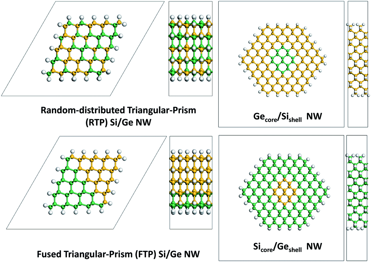 | ||
| Fig. 1 Model structures of randomly distributed triangular-prism (RTP) Si/Ge NW, Gecore/Sishell NW, fused triangular-prism (FTP) Si/Ge NW, random-distributed, and Sicore/Geshell NW, respectively. Color code: Si (gold), Ge (green), H (white). | ||
Computational details and models of SiGe nanowires
Our first-principle calculations were performed within the framework of density functional theory (DFT) as implemented in the Siesta 3.1 code.39 We used a norm-conserving pseudopotential for the core electrons and expanded the one-electron wavefunction of the valence electrons with a double-zeta basis set plus polarization functions. The Perdew–Burke–Ernzerhof (PBE)40 exchange-correlation functional within the generalized gradient approximation (GGA) was employed. A real-space grid with an equivalent cutoff of 180 Ry was adopted to expand the electron density for numerical integration. The periodic boundary condition was applied in all spatial directions, with the vacuum region among NW >15 Å, to neglect the interaction among the periodic images. For the randomly distributed and FTP NW, three unit cells along the axial direction (lattice constants c are about 12.0 Å) were included in the supercell, which ensures that the interaction among the periodic images of the impurity could be neglected.41 For the core/shell NW, supercells containing two unit cells along the axial direction (c ∼ 8.0 Å with which the interaction between periodic images is weak) are selected to reduce computational cost. For structural relaxation, 1 × 1 × 8 and 1 × 1 × 6 meshes within the Monkhorst–Pack special k-point scheme42 in the Brillioun zone were considered for the core/shell and triangular-prism NW, respectively. Denser k grids of 1 × 1 × 16 and 1 × 1 × 12 were used for the core/shell and triangular-prism NW, respectively, in the calculation of electronic structures. Both mesh cutoff and the k points were tested carefully to make sure no significant changes in the total energy when their values are increased.All the SiGe NW are oriented along the 〈110〉 direction (see Fig. 1), i.e., the most common growth orientation for Si and Ge NW.43 The diameter of the core/shell and lateral length scale of the triangular-prism SiGe NW are about 30 Å and 15 Å, respectively. For the core/shell NW, the diameter of the core is about 10 Å. In the triangular-prism NW, all the side surfaces are the {111} crystal planes which ensure high stability of the NW structures. For the core/shell NW, a hexagon-like interface is selected to lower the computational cost. The dangling bonds on the surface are saturated with hydrogen atoms for all the NW, which is an effective way to remove surface states within the band gap of the materials. The lattice constant along the growth orientation and the atomic positions of all the NW are fully relaxed without symmetry constraints, using the conjugate-gradient algorithm. The geometric optimization is completed when the maximum component of the stress tensors and the maximum force on each atom are less than 0.5 GPa and 0.02 eV Å−1, respectively.
Single atomic vacancies of Si and Ge at different sites in the Gecore/Sishell, Sicore/Geshell, FTP and RTP Si/Ge NW are considered. Positions of the vacancies are as shown in Fig. 2. For the segregated Si/Ge NW, i.e., Gecore/Sishell, Sicore/Geshell, and FTP Si/Ge NW, the vacancies near the interface between the Si and Ge parts are mainly considered, while for the RTP Si/Ge NW, the Si (Ge) vacancies with different coordination surroundings are considered, e.g., the vacancies of Si which are coordinated with four Ge atoms, three Ge and one Si, two Ge and two Si, one Ge and three Si, or four Si. For the Gecore/Sishell and Sicore/Geshell NW, five different Si (Ge) vacancies, denoted as VSi1 to VSi5 (VGe1 to VGe5), are studied. For the FTP Si/Ge NW, five Si (Ge) vacancies from the center to the surface of the NW, denoted as VSi1 to VSi5 (VGe1 to VGe5), are investigated. The notations of the vacancies are different for the RTP Si/Ge NW, where VSi0, VSi1, …, VSi4 represents the Si vacancies coordinated with zero, one, …, or four Ge atoms, while VGe0, VGe1, …, VGe4 represents Ge vacancies coordinated with zero, one, …, or four Si atoms. According to our notation scheme, VGe0 and VSi4 in the RTP NW have the same surrounding conditions, i.e., both are surrounded by four Ge atoms. The same conditions are true for VGe1 and VSi3, VGe2 and VSi2, VGe3 and VSi1, VGe4 and VSi0.
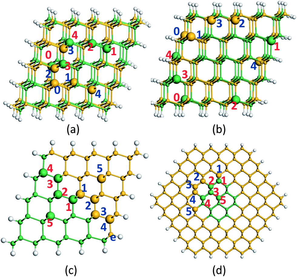 | ||
| Fig. 2 Positions of the vacancies in (a) within the RTP Si/Ge NW (b) surface of the RTP Si/Ge NW (c) the FTP Si/Ge NW, and (d) the Gecore/Sishell NW. Positions of the vacancies of Ge are marked with red numbers, while those of Si are marked with blue numbers. Distribution of the vacancies in the Sicore/Geshell NW is similar to that in the Gecore/Sishell NW. | ||
Results and discussion
1. Relative stabilities of Ge and Si vacancies at different sites
First, we evaluated the relative possibilities of Ge and Si vacancy formation at different sites in the Si/Ge NW by calculating the formation energies of vacancies based on the following formula:| Ef = Etot − Eperfect + μSi (or μGe) |
| Vacancy site | Formation energy (eV) | |||||||||
|---|---|---|---|---|---|---|---|---|---|---|
| Body of RTP NW | VGe0 | VGe1 | VGe2 | VGe3 | VGe4 | VSi0 | VSi1 | VSi2 | VSi3 | VSi4 |
| 2.524 | 2.792 | 2.834 | 3.313 | 2.971 | 3.029 | 2.497 | 2.773 | 2.584 | 2.355 | |
| Surface of RTP NW | VGe0 | VGe1 | VGe2 | VGe3 | VGe4 | VSi0 | VSi1 | VSi2 | VSi3 | VSi4 |
| 1.965 | 2.158 | 2.439 | 2.484 | 2.951 | 2.555 | 2.592 | 2.691 | 2.180 | 2.451 | |
| FTP NW | VGe1 | VGe2 | VGe3 | VGe4 | VGe5 | VSi1 | VSi2 | VSi3 | VSi4 | VSi5 |
| 3.137 | 2.205 | 2.206 | 1.814 | 2.594 | 3.061 | 3.385 | 2.580 | 2.169 | 3.784 | |
| Gecore/Sishell | VGe1 | VGe2 | VGe3 | VGe4 | VGe5 | VSi1 | VSi2 | VSi3 | VSi4 | VSi5 |
| 2.482 | 2.089 | 1.899 | 2.100 | 1.726 | 2.372 | 1.919 | 1.948 | 0.532 | 3.051 | |
| Sicore/Geshell | VGe1 | VGe2 | VGe3 | VGe4 | VGe5 | VSi1 | VSi2 | VSi3 | VSi4 | VSi5 |
| 2.467 | 2.605 | 2.483 | 2.588 | 2.593 | 2.412 | 2.440 | 2.728 | 3.238 | 2.754 | |
For all the Si/Ge NW considered, the formation energies of Si or Ge vacancies are all positive (or endothermic). Thus, the higher the formation energy is, the harder it is for it to form. The formation energies exhibit different trends for different types of NW. For the RTP NW, the formation energies of Si vacancies tend to be a bit lower than those of Ge vacancies under the same surrounding conditions within the body of the NW, namely, VSi1vs. VGe3, VSi2vs. VGe2, VSi3vs. VGe1, VSi4vs. VGe0, except for VSi0vs. VGe4. However, the trend is reversed when the vacancies are on the surface. It is surprising that the formation of the Si vacancy costs less energy than that of Ge under the same surrounding conditions in the body of the RTF NW, even though the bonding strength of Si is usually stronger than that of Ge. A possible reason is that local structural relaxation around the Si vacancy is more substantial and thereby results in more energy gain than that around the Ge vacancy when both are in the body. On the other hand, on the surface, local structural relaxation around either the Si or Ge vacancy is comparable in energy gain, so the effect of the bond strength because of losing an atom is more substantial. Obviously, the formation energies of Ge vacancies have an upward trend with increasing number of surrounding Si atoms, while the trend of the formation energies of Si vacancies is downward with increasing number of surrounding Ge atoms. These trend changes are entirely due to the stronger bonding of Si over Ge. The formation of vacancies on the surfaces is usually easier than that in the body because of higher freedom for the surrounding atoms of the vacancies on the surface than in the body.
For the FTP NW, the formation energies of Si vacancies tend to be a bit higher than those of Ge vacancies at similar sites, again because of the stronger bonding of Si over Ge. When the vacancies are located on the surface, the formation energies tend to decrease. As shown in Table 1, the formation energies of Ge and Si vacancies in the FTP NW are slightly lower than those at similar places (see Fig. 2) in the RTP NW. So, vacancies are easier to generate near the flat interface.
For the core/shell NW, it seems more difficult to generate a vacancy in the core than in the shell, as shown in Table 1, contrary to the trend for the substituted dopants for which the substitution in the core is slightly preferred over the shell.36 Among the four types of Si/Ge NW, formation of vacancies in the Gecore/Sishell NW seems the easiest. The lowest formation energies of Ge and Si vacancies near the interface of the Gecore/Sishell NW are 1.726 and 0.532 eV, respectively (see Table 1). It should be noted that the Gecore/Sishell NW is also the most stable type of Si/Ge NW according to previous calculations.31–33 Thus, it is expected that in the realistic Gecore/Sishell NW more vacancies would be formed at the core/shell interfaces. This is possibly the main reason for the high-density of the hole gas detected in the Gecore/Sishell NW.22–25
2. Electronic structures
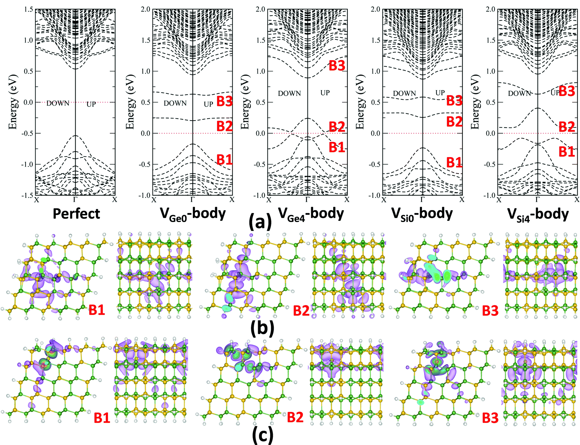 | ||
| Fig. 3 (a) Computed band structures of the RTP Si/Ge NW with a Ge and Si single vacancy in the body. Wavefunction iso-surface of the defect bands near the Fermi level for (b) the VGe0-body, and (c) the VGe4-body. The iso-surface value is 0.05. In (a), Down and Up refer to the spin-up and spin-down channel, respectively. In (b) and (c), the left panel in each pair of panels is axial view while the right panel is side view of the NW. | ||
For the Si vacancy, the band structures of the VSi0-body system are very similar to those of the VGe0-body system. Near the energy gap, there are two localized bands (B2, B3) and one delocalized band (B1) originated from the Si vacancy. The band structures of the VSi4-body system are similar to those of the VGe4-body system. An obvious difference between the band structures of the VSi4-body and the VGe4-body is that the gap between B1 and B2 for the VSi4-body system is a bit larger than that of the VGe4-body system. So, generation of carriers would be a bit harder with the Si vacancies. The band structures of the VSi1-body to the VSi3-body systems are all similar to those of the VSi4-body system (see ESI Fig. S1†).
Interestingly, the band structures of VGe0 and VSi4, and those of VGe4 and VSi0 are quite different while the vacancy surroundings in these systems are the same (four Ge atoms for VGe0 and VSi4, four Si atoms for VSi0 and VGe4, respectively). The local structure relaxation at the vacancy sites may be the main reason for this difference. So the electronic properties of the compositionally-random-distribution SiGe NW can be hard to predict. Relative formation abilities of different vacancies may give some guidance about their electronic properties. Referring to Table 1, because the formation energy of the VGe0-body is the lowest while that of the VGe4-body is the highest, there is a greater possibility that VGe0-body vacancies will be generated. Moreover, for the Si vacancies, the generation of VSi4-body vacancies has the greatest possibility while that of the VSi0-body vacancies is hardest. So, in the RTF NW, if the vacancies are mainly Ge vacancies, the NW should be insulating, while if the vacancies are mainly Si vacancies, the NW would be semiconducting. Generation of the VSi4-body vacancies is slightly easier than the VGe0-body vacancies, so that the defective RTF NW is more likely to be semiconducting if the vacancies are located in the body of the NW.
Next, we studied how the vacancies on the surfaces of the RTP NW influence their electronic structures. The band structures of VGe2-surf and VGe4-surf systems, as well as VSi0-surf and VSi4-surf systems, are shown in Fig. 4. The band structures of other systems are shown in ESI Fig. S2.† From the band structures, one can see that VGe0-surf, VGe1-surf, VGe3-surf and VSi3-surf systems cannot conduct current at low temperatures because the defective bands are strongly localized as in the VGe0-body system. The band structures of VGe2-surf, VSi0-surf, VSi1-surf and VSi2-surf systems are similar to each other and to the band structure of VGe4-body system. The B1 and B2 bands cross one another and also repel each other, resulting in a small band gap (about 0.2 eV in this case). The Fermi level is just located within the small band gap, implying that holes can be generated at finite temperatures. In summary, all these vacancy systems show p-type semiconducting properties.
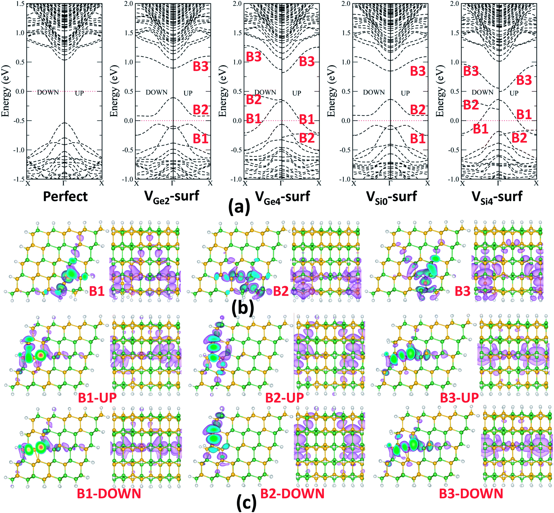 | ||
| Fig. 4 (a) Computed band structures of the RTP Si/Ge NW with a Ge and Si single vacancy on the surface. Wavefunction iso-surface of the defect bands near the Fermi level for (b) the VGe2-surf, and (c) the VGe4-surf systems. The iso-surface value is 0.05. In (a), Down and Up refer to the spin-up and spin-down channel, respectively. In (b) and (c), the left panel in each pair of panels is axial view while the right panel is side view of the NW. | ||
A very different and interesting behavior was also noticed in the band structures of the VGe4-surf and VSi4-surf systems. As shown in Fig. 4, the Fermi level crosses the B1 band for both systems. Because the B1 band suggests that there will be good conductivity because of the extensively delocalized distribution of the wavefunctions along the axial direction, VGe4-surf and VSi4-surf NW are predicted to be conductors. Moreover, the spin polarized B2 band splits and the spin-down band moves up relatively. In contrast to the VGe2-surf and VSi0-surf systems, there is no gap opening between bands B1 and B2 for the VGe4-surf and VSi4-surf systems. The reason for the spin splitting may be the strong repulsion between the conduction band B1 and the non-conduction band B2. Interestingly, the spin splitting only occurs in the VGe4-surf and VSi4-surf systems, in which the vacancy sites are surrounded by four Si atoms or four Ge atoms, and this only occurs for the highly localized B2 bands.
Note also that the formation energies of VGe0-surf and VGe1-surf vacancies are obviously lower than those of other Ge vacancies, and the formation energy of VSi3-surf is obviously lower than those of other Si vacancies. For VGe0-surf, VGe1-surf, and VSi3-surf systems, computed band structures show that they are all insulators. Thus, the vacancies on the surface of a RTF NW are of no help to the conductivity of the NW.
Seong et al. reported that the synthesized SixGe1−x NW exhibit a p-type feature and they attributed this feature to the oxidation of Ge at the interfaces between SixGe1−x and SiOx oxidation surfaces.21 According to our calculations, the point vacancy defect may be another reason for their p-type semiconducting properties. The contribution of the vacancies to the p-type semiconducting properties was not considered in ref. 21 because the density of vacancies is much lower compared to that which is seen in oxidation. For an oxidation-free SixGe1−x NW, the vacancies can lead to p-type semiconducting properties.
 | ||
| Fig. 5 Computed band structures of the FTP Si/Ge NW with a Ge and a Si single vacancy at various sites. | ||
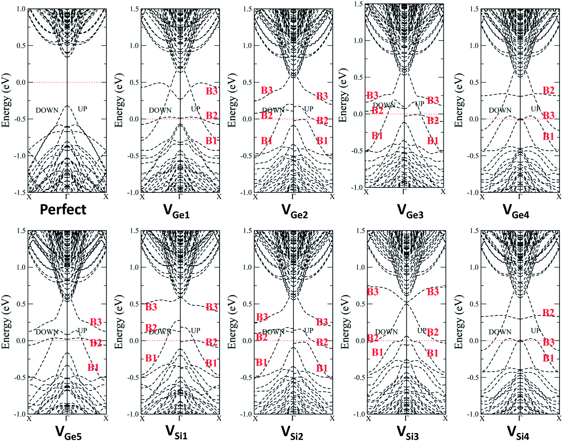
As seen in Fig. 5, in most systems, the vacancies in the FTP Si/Ge NW introduce three defect bands within the band gap of the perfect FTP/SiGe NW. The electronic properties of each defect band can be understood from their wavefunction distributions. In Fig. 6, the wavefunction iso-surfaces corresponding to the defect bands of VGe1, VGe4, VSi1 and VSi4 systems are shown. Apparently, in all systems, B1 bands correspond to the conducting bands as the band lines disperse over extensive energy ranges and the associated wave functions are delocalized along the axial direction. Furthermore, for most systems the B1 band should lead to hole conduction because their band lines tilt downwards from the center of the first Brillouin zone to the surface (Γ to X), except for those of the VSi4 system. The B2 bands for all systems are normally very flat and localized. As shown in Fig. 6, the wavefunctions of the B2 band are distributed dispersedly along the interface, but are localized along the axial direction. So, the B2 bands for all systems cannot lead to carrier conduction. The wavefunctions of the B3 bands are also mainly localized around the vacancy sites, and exhibit little delocalization along the axial direction in some systems. So, the B3 bands may give minor conduction of holes or electrons.
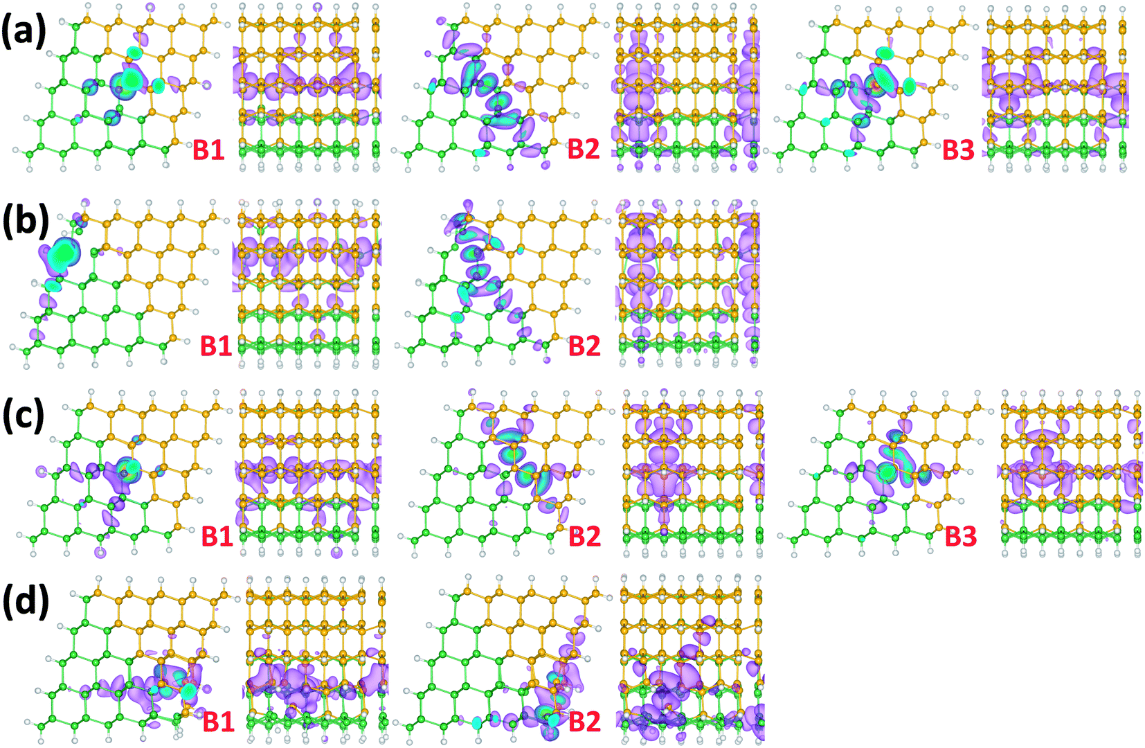 | ||
| Fig. 6 Computed wavefunction iso-surface corresponding to the defect bands for the (a)VGe1, (b) VGe4, (c) VSi1 and (d) VSi4 vacancy in the FTP Si/Ge NW. The iso-surface value is 0.05. The left panel in each pair of panels is axial view while the right panel is side view of the NW. | ||
In addition, spin splitting is seen for the VGe1, VGe5, VSi1, VSi2 and VSi5 systems but not others. Again, the spin splitting mainly occurs in the highly delocalized B2 bands. For some systems, the B3 bands exhibit spin splitting too. The Fermi levels for these five systems all cross the corresponding conduction B1 bands. For the VGe2, VGe3 and VGe4 systems, Fig. 5 clearly shows that the Fermi levels cross both the top valence band and the B1 defect band, resulting in carrier conduction. The B2 and B3 bands for the VGe4 system are very high compared to those for other Ge vacancy systems. The B3 band (not marked in Fig. 5) even merges with the conduction bands for the VGe4 system. For the VSi3 system, the maximum of the valence band and the minimum of the B2 band are almost the same. The Fermi level is just located above the maximum of the valence band. So, the VSi3 system may also have good conductivity.
Again, VSi4 system is quite different. As shown in Fig. 5, the B1 band for the VSi4 system is close to the conduction bands and tilts upwards, suggesting that there is good conductivity of the electrons but not the holes. Both B1 and B2 bands are located very high, far from the top valence band. A relatively big band gap (∼0.5 eV) is seen between the top valence band and the B1 band, and the Fermi level is located at the center of the gap. Contrary to other systems, the VSi4 system is an insulator at low temperatures. As shown in Fig. 6(d), the wavefunctions of the B2 band for the VSi4 system are mainly contributed by the vacancy states and the surface states, but not the interface states.
In summary, with vacancies in the FTP Si/Ge NW, except in the VSi4 system, all the systems are semiconducting. Because the formation of Ge vacancies is easier than that of Si vacancies in the FTP Si/Ge NW, the defective FTP Si/Ge NW is likely to have a high possibility of exhibiting p-type semiconducting properties.
 | ||
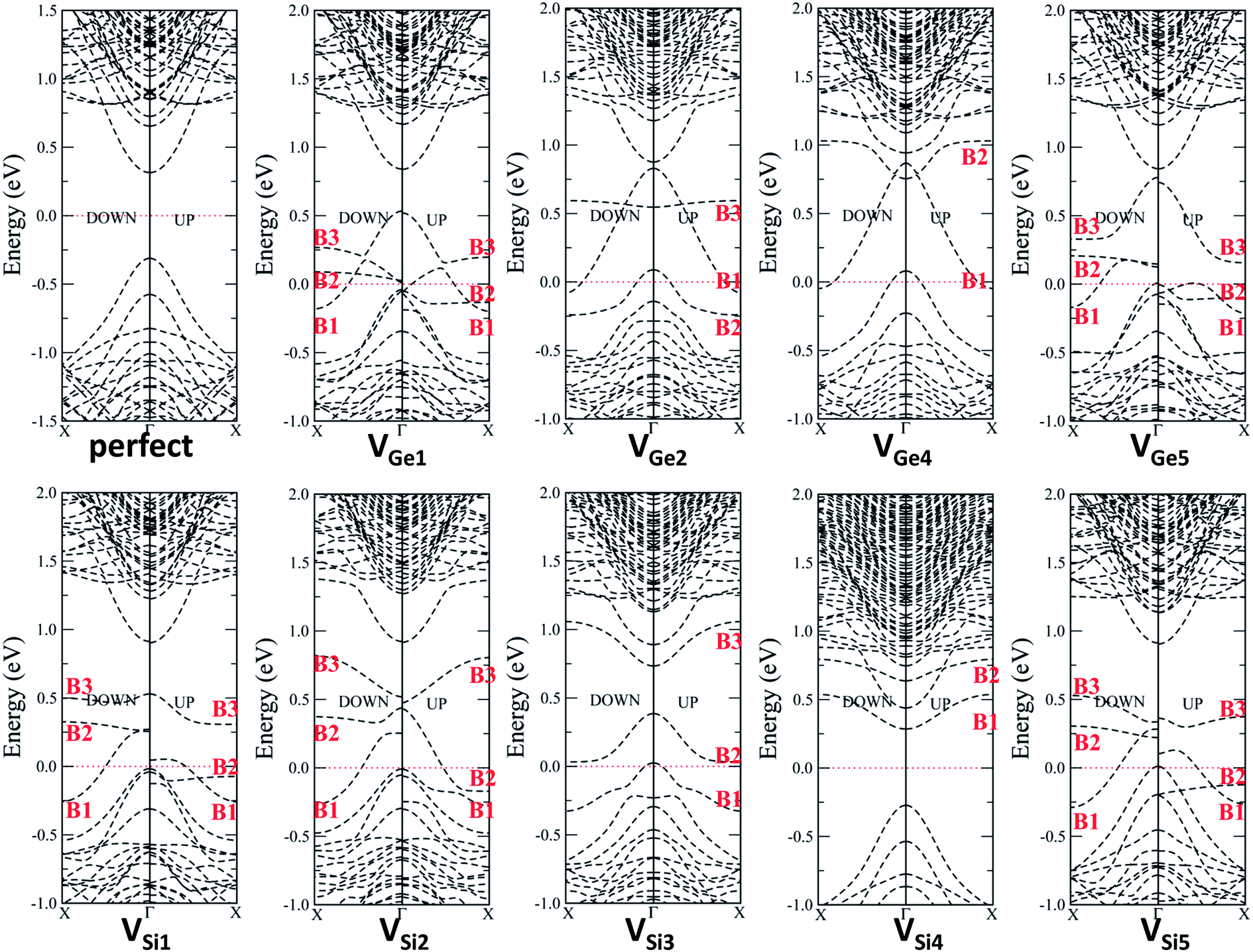
| Fig. 7 Computed band structures of the Gecore/Sishell NW with a Ge and Si single vacancy at various sites in the intersection area. | ||
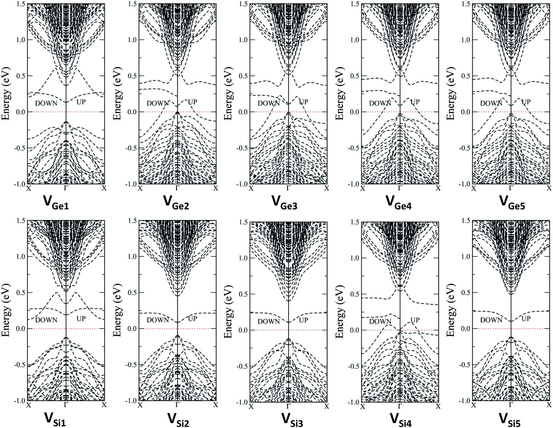
Compared to the band structures of the perfect Gecore/Sishell NW, one can easily see that the defects result in three bands in the gap region, called B1, B2, and B3 bands according to their wavefunction distributions (Fig. 8). The B1 band is highly delocalized. It disperses over the band gap for the Gecore/Sishell NW. So, it is a conducting band. Because it tilts downwards along the direction Γ → X, the conducting carriers should be holes. The B2 band is the flattest among the three defect bands. It is also localized and cannot lead to carrier conduction. The wavefunctions of the B2 band are localized along the axial direction and slightly delocalized along the radial direction. The wavefunction distribution of the B3 band is between those of the B1 and B2 bands. In some cases, it is quite flat while in other cases it is not. Normally, the B3 band tilts upwards firstly and then turns downwards, along the direction Γ → X in the Brillouin zone. Because of the high localization, in some systems, the spin polarized B2 and B3 bands are split.
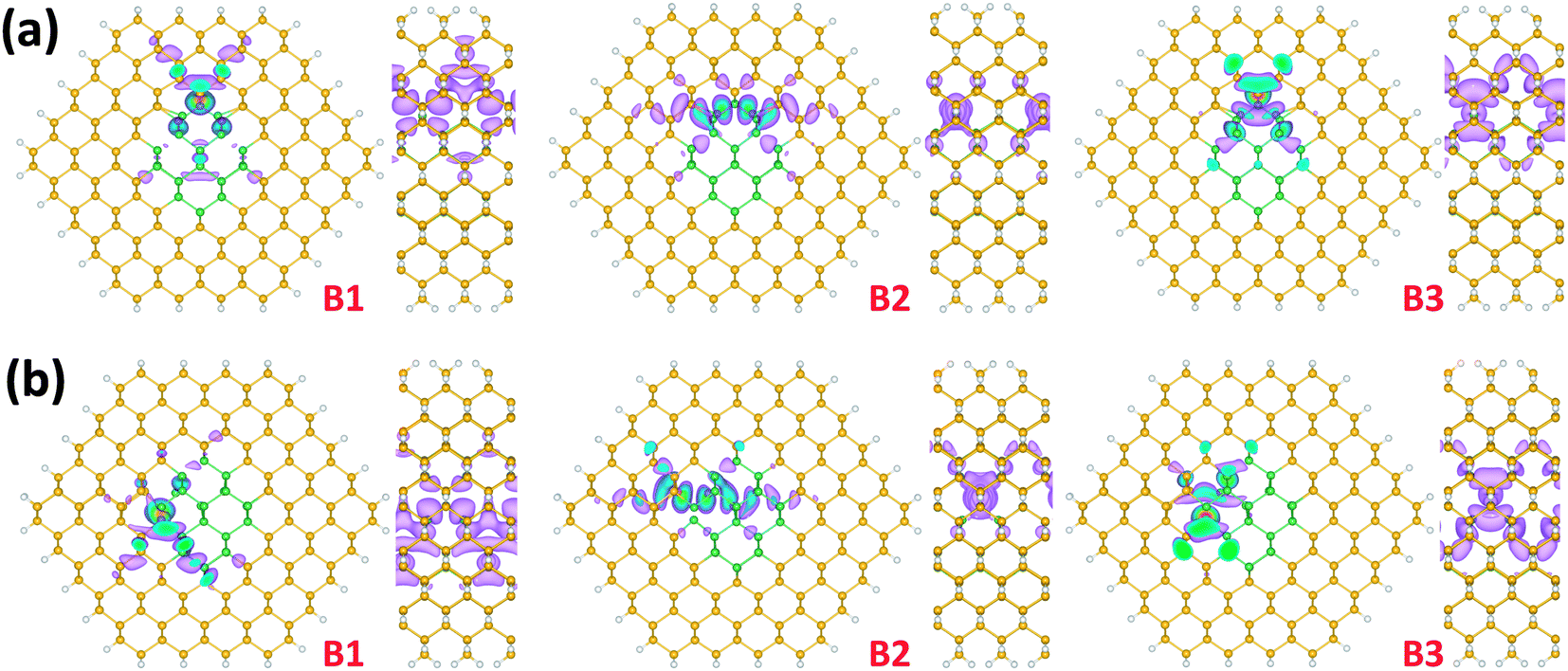 | ||
| Fig. 8 Computed wavefunction iso-surface of the defect bands for (a) VGe1, and (b) the VGe4 vacancy in the Gecore/Sishell NW. The iso-surface value is 0.05. The left panel in each pair of panels is axial view while the right panel is side view of the NW. | ||
For all systems, the Fermi levels cross at least the B1 band. Because the B1 band suggests high conductivity for holes, all the systems should have good conductivities. In experiments, a high density of hole carriers are found in the core of the Gecore/Sishell NW.22–25 Park et al.28 studied the Si dangling bond on the surface and the Au impurity within the Si shell of the Gecore/Sishell NW to explain why a high density of holes is present in the Gecore/Sishell NW. However, the dangling bonds at the interfaces were not considered. Vacancies are expected to be formed more easily at the interfaces than in the inner part of core or shell during the growth, because of the mismatch of the lattice constants and the constraint stresses. The hole carriers generated due to the ionization of the vacancies at the interfaces are easier to transfer to the core region, compared to those generated on the surfaces. Therefore, the vacancies at the interfacial region of the Gecore/Sishell NW are more likely to give rise to a high-density hole gas as demonstrated experimentally.
For the Sicore/Geshell NW, the difference in stress at the interface region makes the band structures of Sicore/Geshell NW much different from those of the Gecore/Sishell NW (see Fig. 9). Apparently, with the Ge vacancies, most systems are still conducting, except for the VGe1 system which is not. However, with the Si vacancies, all the systems are not conducting because of the lack of band crossing through the Fermi level. By comparing the band structures of the Sicore/Geshell NW and the Gecore/Sishell NW, one can see that for the non-conducting systems, the B1 band is either shifted upwards, leaving a big gap from the Fermi level, or downwards into the valence bands. For the conducting systems, VGe2 to VGe5 and VSi4, the formation energies of the vacancies are all much higher than those for the Gecore/Sishell NW. So vacancies in the Sicore/Geshell NW are not as important a contribution as those in the Gecore/Sishell NW to the conductivity.
 | ||
| Fig. 9 Computed band structures of the Sicore/Geshell NW with a Ge and Si single vacancy at various sites in the intersection area. | ||
Conclusion
We have studied the effects of single vacancies on semiconducting properties of four different types of SiGe NW, i.e., RTP NW, the FTP NW, the GecoreSishell and the SicoreGeshell NW. Si and Ge vacancies at different sites are investigated. The calculated formation energies indicate that the formation tendency of single Si or Ge vacancies is strongly dependent on the structures of the NW. The formation of vacancies at the interface of the GecoreSishell NW entails least energy among all the NW considered. The computed band structures suggest that the defective RTP, FPT and GecoreSishell NW exhibit p-type semiconducting properties, whereas the semiconducting properties of the defective SicoreGeshell NW are much less apparent. For the RTP NW, the hole-carriers are likely originated from the Si vacancies located in the inner area, while in the FPT and GecoreSishell NW both the Si and Ge vacancies at the interfaces can generate high-density hole carriers. The hole injection in the GecoreSishell NW is likely to be the easiest among all the NW considered. Our theoretical results are consistent with experimental observations, thereby providing a compelling explanation on why the experimentally synthesized Si1−xGex and GecoreSishell NW can exhibit remarkable p-type semiconducting properties without relying on any doping strategy.Acknowledgements
This work is supported by the National Natural Science Foundation of China (Grant no. 11104056), the Natural Science Foundation of Anhui Province (Grant no. 11040606Q33). XCZ is supported by ARL (Grant no. W911NF1020099) and a grant from USTC for (1000 Talents Program) Qianren-B summer research.References
- D. D. D. Ma, C. C. Lee, F. C. K. Au, S. Y. Tong and S. T. Lee, Science, 2003, 299, 1874–1877 CrossRef CAS PubMed.
- Y. Cui and C. M. Lieber, Science, 2001, 291, 851–853 CrossRef CAS PubMed.
- J. Xiang, W. Lu, Y. J. Hu, Y. Wu, H. Yan and C. M. Lieber, Nature, 2006, 441, 489–493 CrossRef CAS PubMed.
- T. J. Kempa, B. Z. Tian, D. R. Kim, J. S. Hu, X. L. Zeng and C. M. Lieber, Nano Lett., 2008, 8, 3456–3460 CrossRef CAS PubMed.
- S. W. Nam, X. C. Jiang, Q. H. Xiong, D. Ham and C. M. Lieber, Proc. Natl. Acad. Sci. U. S. A., 2009, 106, 21035–21038 CrossRef CAS PubMed.
- Y. Cui, Q. Q. Wei, H. K. Park and C. M. Lieber, Science, 2001, 293, 1289–1292 CrossRef CAS PubMed.
- P. Alivisatos, Nat. Biotechnol., 2004, 22, 47–52 CrossRef CAS PubMed.
- G. F. Zheng, F. Patolsky, Y. Cui, W. U. Wang and C. M. Lieber, Nat. Biotechnol., 2005, 23, 1294–1301 CrossRef CAS PubMed.
- J. Hahm and C. M. Lieber, Nano Lett., 2004, 4, 51–54 CrossRef CAS.
- F. Patolsky, G. F. Zheng, O. Hayden, M. Lakadamyali, X. W. Zhuang and C. M. Lieber, Proc. Natl. Acad. Sci. U. S. A., 2004, 101, 14017–14022 CrossRef CAS PubMed.
- W. U. Wang, C. Chen, K.-H. Lin, Y. Fang and C. M. Lieber, Proc. Natl. Acad. Sci. U. S. A., 2005, 102, 3208–3212 CrossRef CAS PubMed.
- M. Amato, M. Palummo, R. Rurali and S. Ossicini, Chem. Rev., 2014, 114, 1371–1412 CrossRef CAS PubMed.
- M. Amato, S. Ossicini and R. Rurali, Nano Lett., 2012, 12, 2717–2721 CrossRef CAS PubMed.
- L. Zhang, M. d'Avezac, J.-W. Luo and A. Zunger, Nano Lett., 2012, 12, 984–991 CrossRef CAS PubMed.
- T. Markussen, Nano Lett., 2012, 12, 4698–4704 CrossRef CAS PubMed.
- J. E. Yang, C. B. Jin, C. J. Kim and M. H. Jo, Nano Lett., 2006, 6, 2679–2684 CrossRef CAS PubMed.
- X. Zhang, K.-K. Lew, P. Nimmatoori, J. M. Redwing and E. C. Dickey, Nano Lett., 2007, 7, 3241–3245 CrossRef CAS PubMed.
- C. Qi, G. Goncher, R. Solanki and J. Jordan, Nanotechnology, 2007, 18, 075302 CrossRef PubMed.
- U. Givan and F. Patolsky, Nano Lett., 2009, 9, 1775–1779 CrossRef CAS PubMed.
- T. Shimizu, Z. Zhang, S. Shingubara, S. Senz and U. Gösele, Nano Lett., 2009, 9, 1523–1526 CrossRef CAS PubMed.
- H. K. Seong, E. K. Jeon, M. H. Kim, H. Oh, J. O. Lee, J. J. Kim and H. J. Choi, Nano Lett., 2008, 8, 3656–3661 CrossRef CAS PubMed.
- J. Xiang, W. Lu, Y. J. Hu, Y. Wu, H. Yan and C. M. Lieber, Nature, 2006, 441, 489–493 CrossRef CAS PubMed.
- W. Lu, J. Xiang, B. P. Timko, Y. Wu and C. M. Lieber, Proc. Natl. Acad. Sci. U. S. A., 2005, 102, 10046–10051 CrossRef CAS PubMed.
- S. X. Zhang, F. J. Lopez, J. K. Hyun and L. J. Lauhon, Nano Lett., 2010, 10, 4483–4487 CrossRef CAS PubMed.
- L. Y. Li, D. J. Smith, E. Dailey, P. Madras, J. Drucker and M. R. McCartney, Nano Lett., 2011, 11, 493–497 CrossRef CAS PubMed.
- L. Yang, R. N. Musin, X. Q. Wang and M. Y. Chou, Phys. Rev. B: Condens. Matter Mater. Phys., 2008, 77, 195325 CrossRef.
- A. Nduwimana, R. N. Musin, A. M. Smith and X. Q. Wang, Nano Lett., 2008, 8, 3341–3344 CrossRef CAS PubMed.
- J. S. Park, B. Ryu, C. Y. Moon and K. J. Chang, Nano Lett., 2010, 10, 116–121 CrossRef CAS PubMed.
- M. Amato, M. Palummo and S. Ossicini, Mater. Sci. Eng., B, 2012, 177, 705–711 CrossRef CAS PubMed.
- M. Palummo, M. Amato and S. Ossicini, Phys. Rev. B: Condens. Matter Mater. Phys., 2010, 82, 073305 CrossRef.
- M. Amato, M. Palummo and S. Ossicini, Phys. Rev. B: Condens. Matter Mater. Phys., 2009, 80, 235333 CrossRef.
- M. Amato, M. Palummo and S. Ossicini, Phys. Rev. B: Condens. Matter Mater. Phys., 2009, 79, 201302 CrossRef.
- M. Amato, M. Palummo and S. Ossicini, Phys. Status Solidi B, 2010, 247, 2096–2101 CrossRef CAS.
- M. Amato, S. Ossicini and R. Rurali, Nano Lett., 2011, 11, 594–598 CrossRef CAS PubMed.
- M. Amato, M. Palummo and S. Ossicini, J. Comput. Electron., 2012, 11, 272–279 CrossRef CAS.
- P. Li, R. Zhou and X. C. Zeng, Nanoscale, 2013, 5, 3880–3888 RSC.
- N. Fukata, M. Mitome, T. Sekiguchi, Y. Bando, M. Kirkham, J. Hong, Z. L. Wang and R. L. Snyder, ACS Nano, 2012, 6, 8877–8895 Search PubMed.
- D. C. Dillen, K. Kim, E.-S. Liu and E. Tutuc, Nat. Nanotechnol., 2014, 19, 116–120 CrossRef PubMed.
- D. S. Portal, P. Ordejon, E. Artacho and J. M. Soler, Int. J. Quantum Chem., 1997, 65, 453–461 CrossRef.
- J. P. Perdew and A. Zunger, Phys. Rev. B: Condens. Matter Mater. Phys., 1981, 23, 5048–5079 CrossRef CAS.
- E. Durgun, N. Akman, C. Ataca and S. Ciraci, Phys. Rev. B: Condens. Matter Mater. Phys., 2007, 76, 245323 CrossRef.
- H. J. Monkhorst and J. D. Pack, Phys. Rev. B: Solid State, 1976, 13, 5188–5192 CrossRef.
- Y. Wu, Y. Cui, L. Huynh, C. J. Barrelet, D. C. Bell and C. M. Lieber, Nano Lett., 2004, 4, 433–436 CrossRef CAS.
Footnote |
| † Electronic supplementary information (ESI) available: Computed band structures of the random-distributed triangular-prism (RTP) Si/Ge NW with Ge and Si single vacancy in the body and on the surface. See DOI: 10.1039/c4tc00958d |
| This journal is © The Royal Society of Chemistry 2014 |