 Open Access Article
 This Open Access Article is licensed under a
 Creative Commons Attribution 3.0 Unported Licence
Heteroatom modified graphenes: electronic and electrochemical applications
Martin
Pumera
*
Division of Chemistry & Biological Chemistry, School of Physical and Mathematical Sciences, Nanyang Technological University, 637371, Singapore. E-mail: pumera@ntu.edu.sg; pumera.research@outlook.com
First published on 2nd July 2014
Abstract
Graphene exhibits zero band gap, very small electrical resistivity, fast heat dissipation, and fast heterogeneous electron transfer properties. These features, coupled with affordable preparation cost and high surface area, predetermine graphene materials for application in electronic and electrochemical devices. Doping graphene with electron-withdrawing or -donating heteroatoms leads to tailoring of graphene electronic and electrochemical properties. Here, we discuss doping of graphene-based materials with main group heteroatoms (s and p blocks). We will also discuss the application of such doped graphenes in electronic, sensing, and energy storage/generation devices.
 Martin Pumera | Prof. Martin Pumera has been a faculty member at Nanyang Technological University, Singapore since 2010. He received his PhD at Charles University, Czech Republic, in 2001. After two postdoctoral stays (in the USA and Spain), he joined the National Institute for Materials Science, Japan, in 2006 for a tenure-track arrangement and stayed there until Spring 2008 when he accepted a tenured position at NIMS. In 2009, Prof. Pumera received an ERC-StG award. Prof. Pumera has broad interest in nanomaterials and microsystems, in the specific areas of electrochemistry and synthetic chemistry of carbon nanomaterials, nanomotors, nanotoxicity, and energy storage devices. He is an associate editor of Science and Technology of Advanced Materials, and a member of Editorial board of Chem.–Eur. J., Electrochem. Commun., Electrophoresis, Electroanalysis, The Chemical Records, ChemElectroChem and eight other journals. He has published over 270 peer-reviewed articles and has h-index 44. |
1. Introduction
Graphene exhibits zero band gap and fast electron transfer at the defect sites/edges of the sheets.1,2 By doping graphene with heteroatoms, one can tailor the band gap by providing or withdrawing electrons from the graphene structure and by providing electrochemically active/inactive sites. Here, we will discuss doping of graphene with main group elements, that is, with group I A to VII A (s- and p-block) including hydrogen. We intentionally excluded transition metals (d-block elements). In addition, we will discuss the methods of preparation of doped graphenes because these methods have a strong influence on the way the heteroatom is implanted into the graphene and on its properties. We will also discuss theoretical studies; however, the main focus of the article will be on experimental studies.2. Group I A: alkali metals
Potassium-doped graphene oxides exhibited faster electron transfer rates towards ferro/ferricyanide than did non-doped graphene oxides. Graphite oxide, prepared by the Hummers or Hofmann method, was mixed with metallic (elemental) potassium in a glove box and subjected to thermal exfoliation. The resulting materials contained ∼0.5 at% of K and also a much higher amount of oxygen-containing groups than those of the control experiment in the absence of elemental K. The reason is that potassium is bonded in alcoholates and thus prevents these groups from vaporization. Despite a larger amount of oxygen-containing groups, the K-doped graphene oxide exhibited faster heterogeneous electron transfer than did the control sample of thermally reduced graphene oxide.3 It also showed an electrocatalytic effect towards the reduction of NO2− and SO32− ions.43. Group II A: alkaline earth metals
Doping graphene by the second main group (II A) to alter electronic or electrochemical properties is very rare. In a theoretical and experimental study on the electron transport properties of Ca-doped graphene, it was concluded that the theoretical results significantly differed from the measurements.5 There is certainly much more to do in the field of doping graphene with second main group elements, as they show strong interactions with oxygen-containing groups of graphene oxide; such interaction gains intensity with increasing atomic weight of the II A group element.64. Group III A: the boron group
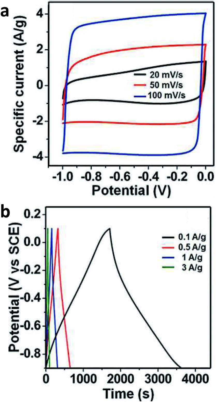
Boron is a common atom for doping graphene for electrochemical and electronic purposes. In general, boron is considered a p-type dopant. However, this is only true if the boron atom is integrated into the graphene lattice. When boron is incorporated as a –BH2 group, the electron-withdrawing effect is not strong. There are different methods of doping graphene with boron. The synthetic methodology influences the way boron is incorporated and thus the resulting electronic and electrochemical properties. Hydroboration with BH3 in tetrahydrofuran leads to –BH2 group doped graphenes as this mechanism prohibits direct doping of the graphene lattice and it is a simple addition reaction on the C![[double bond, length as m-dash]](https://www.rsc.org/images/entities/char_e001.gif) C bond (Fig. 1).7 Such graphenes exhibited high electrochemical weight capacitance (Fig. 2).8 Boron was doped by the thermal exfoliation/reduction of graphite oxide (which was prepared by the Staudenmaier method) in a BF3 atmosphere at 800 °C. In such a case, boron was directly incorporated into the graphene lattice.9 Such graphene demonstrated fast heterogeneous electron transfer, faster than for N-doped graphene. Similarly, B-doped graphene exhibited higher electrical conductivity than did N-doped graphene.9 Graphenes doped with increasing amounts of boron in their lattice showed inhibition of ORR with increased amounts of B as well as decreased capacitance.10 This is opposite to graphene doped with boron groups in the –BH2 form.8 The role of B (and N) doping in increasing the capacitance of graphene was recently questioned.11 B-doped graphenes exhibited higher resistance to electrode fouling during electrochemical analysis of biomarkers when compared to undoped graphene materials.12 In other reports, it was claimed that boron was doped by heating B2O3 at 1200 °C with graphene oxide. One should note that B2O3 sublimes (and does not decompose to B and O) at ∼1500 °C. In this work, electrocatalysis towards an oxygen reduction reaction was reported.13 In a different study, H3BO3 was heated to 900 °C in the presence of graphene, doping by B and electrocatalysis of ORR were reported.14 In a similar manner, at this temperature, H3BO3 loses water and transforms into B2O3.15
C bond (Fig. 1).7 Such graphenes exhibited high electrochemical weight capacitance (Fig. 2).8 Boron was doped by the thermal exfoliation/reduction of graphite oxide (which was prepared by the Staudenmaier method) in a BF3 atmosphere at 800 °C. In such a case, boron was directly incorporated into the graphene lattice.9 Such graphene demonstrated fast heterogeneous electron transfer, faster than for N-doped graphene. Similarly, B-doped graphene exhibited higher electrical conductivity than did N-doped graphene.9 Graphenes doped with increasing amounts of boron in their lattice showed inhibition of ORR with increased amounts of B as well as decreased capacitance.10 This is opposite to graphene doped with boron groups in the –BH2 form.8 The role of B (and N) doping in increasing the capacitance of graphene was recently questioned.11 B-doped graphenes exhibited higher resistance to electrode fouling during electrochemical analysis of biomarkers when compared to undoped graphene materials.12 In other reports, it was claimed that boron was doped by heating B2O3 at 1200 °C with graphene oxide. One should note that B2O3 sublimes (and does not decompose to B and O) at ∼1500 °C. In this work, electrocatalysis towards an oxygen reduction reaction was reported.13 In a different study, H3BO3 was heated to 900 °C in the presence of graphene, doping by B and electrocatalysis of ORR were reported.14 In a similar manner, at this temperature, H3BO3 loses water and transforms into B2O3.15
 | ||
| Fig. 1 Boron doping of graphene by hydroboration (resulting in addition of a –BH2 group to the graphene structure). (A) BH3–THF adduct and (B) preparation of boron-doped graphene. (C) General scheme of hydroboration of CC. (A and B) reprinted with permission from ref. 8. | ||
 | ||
| Fig. 2 Boron-doped graphene for supercapacitors. The electrochemical performance of a B-rG-O electrode in 6 M KOH solution using a two-electrode configuration, showing (a) CV curves at various scan rates, line segments connecting points added as a guide to the eye, and (b) galvanostatic charge/discharge curves at different current densities. Reprinted with permission from ref. 8. | ||
5. Group IV A: carbon group
It has been calculated that doping graphene with IV group elements (carbon group) increases its band gap to 2.13 eV for Si, while when doped with Ge or Sn, the band gap is about half of this value.16 Doping graphene with these elements is very rare; it is certainly an interesting area for investigation. It should be mentioned that Si strongly dopes the graphene layer that is in contact with the Si wafer. However, it does not influence the electronic properties of subsequent layers.176. Group V A: pnictogens
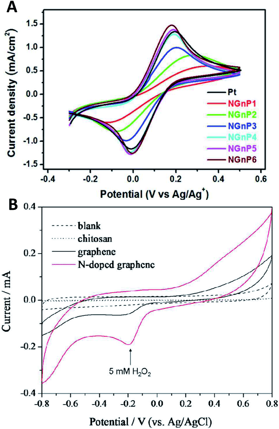
Group V A elements are, in principle, electron donors. However, similar to group III A, the electron-donating/withdrawing effect depends on the chemical bonding arrangement.18 Nitrogen doping is very widely used for tailoring the electronic and electrochemical properties of graphene. Nitrogen can be incorporated into the graphene lattice in various forms, such as quaternary nitrogen, pyridinic N, pyrrolic N, aromatic amine, hydroazone, pyrazole and pyrazoline groups; these groups can exhibit completely contrasting electronic properties, such as an electron-donating group (amine) or as an electron-withdrawing group (quaternary nitrogen), see Fig. 3. Even though the way nitrogen is incorporated into the graphene lattice significantly influences the properties of the doped graphene, it is difficult to gain full control over the chemical configuration of the doped nitrogen. Nitrogen-doped graphenes were demonstrated to act as electrocatalysts for hydrogen peroxide reduction, which is very important in biosensing applications. Nitrogen-doped graphenes showed fast heterogeneous electron transfer (HET) rates to Co(bpy)33+/2+ which is immensely important for applications in solar cells; the HET rates increased with the increased level of N doping, as indicated in Fig. 4A.19 Nitrogen-doped graphenes also exhibited higher currents for hydrogen peroxide reduction, which is of very high importance in the biosensing set-up, where H2O2 is often an enzymatic product (Fig. 4B).20 N-doped graphenes were reported to be very powerful for ORR.21 It was suggested that quaternary nitrogen plays a major role in ORR.22 Co-doped B and N graphenes reportedly exhibit even higher electrocatalysis for ORR.23 N-doped graphene was also shown to exhibit high capacitance.24,25 It was demonstrated that such increased capacitance is due to the so-called quantum capacitance.26 N-doped graphene was also shown to be a superior metal-free counter electrode in organic dye-sensitized solar cells19 as well as a metal-free electrode for electrocatalytic water oxidation.27 | ||
| Fig. 3 Nitrogen-doped graphene containing various groups which are either electron-donating or electron-withdrawing. Some of these groups are shown in the scheme above. Note that reduction of graphene oxide with hydrazine will dope the graphene with nitrogen containing moieties which are shown in blue color. (A) Quaternary nitrogen; (B) pyridinic N; (C) pyrrolic N; (D) aromatic amine; (E) hydroazone; (F) pyrazole and (G) pyrazoline groups at the graphene fragment. | ||
 | ||
| Fig. 4 Electrochemistry at nitrogen-doped graphenes. (A) Cyclic voltammograms obtained at a scan rate of 10 mV s−1 for the oxidation and reduction of the Co(bpy)33+/2+ redox couple using the Pt and NGnP working electrodes, in 0.1 M LiClO4; increasing numbers at labels indicate increasing doping levels. (B) Hydrogen peroxide reduction is catalyzed at N-doped graphene. Reprinted with permission from ref. 19 and 20, respectively. | ||
Phosphorus was doped into graphene by mixing graphene oxide with phosphoric acid and drying, which was reported to have an electrocatalytic effect in ORR.28 It is possible to simultaneously reduce GO and dope with phosphorus via refluxing it with P4/KOH.29
7. Group VI A: chalcogens
Oxygen is very often part of graphene structure because one of the main routes of graphene synthesis is via graphite oxide,30–32 graphene oxide with consecutive reduction. Oxygen moieties on graphene are considered unwanted and major efforts are being made to remove them.33 The oxygen-containing groups present on the graphene surface are of a wide variety, both electron withdrawing and donating. These include hydroxyl, aldehyde, ketone, peroxide, epoxide, carbonyl, ester, lactone, etc.34 It is extremely challenging to selectively remove/introduce particular groups.35 It was demonstrated that heterogeneous electron transfer rates increase with a decrease in the amount of oxygen-containing groups.36 It is possible to tune the amount of oxygen-containing groups (epoxy, peroxy, and aldehyde) by electrochemical reduction and consequently tuning HET rates.37 The electrical conductivity of graphene oxide increases upon the removal of oxygen from the graphene structure; this is the basis for claims of the restoration of sp2 CC bonds upon removal of these groups. However, the real reason for increased conductivity is not fully known.
Sulfur-doped graphenes can be fabricated by either thermal exfoliation of graphite oxide in sulfur-containing gas (i.e., H2S, CS2 or SO2)38 or by carbonizing graphene with organic molecules containing sulfur, i.e., styrene sulfonate or benzyl disulfide.39,40 The amount of sulfur incorporated into the graphene lattice by the method using graphite oxide and H2S, CS2 or SO2 gas as precursors for thermal exfoliation/doping depends mostly on the method the graphite oxide was prepared (whether by Hummers, Hofmann, or Staudenmaier method) rather than on the type of gas (Fig. 5a).
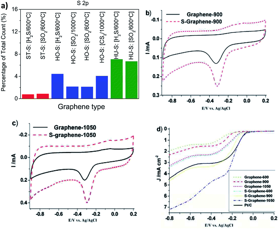 | ||
| Fig. 5 Sulfur doping of graphene. (a) Exfoliation of graphite oxide (ST, Staudenmaier; HO, Hofmann; HU, Hummers) in sulfur containing gas (CS2, H2S or SO2). It is obvious that the amount of sulfur doped depends more on the starting graphite oxide than on the sulphur containing gas composition. (b–d) Oxygen reduction on sulfur-doped graphenes (number codes associated with graphene are related to the annealing temperature which influences the final composition of S-doped graphene and its performance); (b) graphene-900 and S-graphene-900, and (c) graphene-1050 and S-graphene-1050; (d) linear scanning voltammograms of various graphenes and a Pt/C catalyst on a glass carbon rotating disk electrode saturated in O2 at a rotation rate of 1600 rpm. Reprinted with permission from ref. 38 (a) and ref. 40 (b–d). | ||
When the amount of sulfur in the graphene lattice was increased, the electrical resistivity increased as well.38 During exfoliation in an atmosphere containing sulfur gas, different sulfur-containing moieties, such as –SH or –SO3−, are introduced, depending on the exfoliation conditions. Increased capacitance of sulfur-doped graphenes compared to undoped ones was reported.39 Sulfur-doped graphenes were also shown to act as metal-free electrocatalysts for oxygen reduction (Fig. 5b–d).40 Graphenes co-doped with both sulfur and nitrogen also show electrocatalytic effects towards oxygen reduction.41,42 Selenium-doped graphene also exhibited electrocatalysis in ORR.43
8. Group VII A: halogens
Halogen atoms exhibit both the electron-withdrawing effect due to electronegativity and the resonance donating effect due to the existence of lone pair of electrons. The electronic structure of graphene changes significantly depending on the halogen atom. Fluorinated graphene has a wide band gap of 3.1 eV, while chlorinated graphene has a much smaller band gap of 0.9 eV and brominated graphene has almost zero band gap (Fig. 6).44 It was found experimentally that with increasing halogen size (and decreasing electronegativity), the electrical resistivity of halogen-doped graphene decreases;44,45 this is consistent with theoretical results. | ||
| Fig. 6 Halogenation of graphene changes its electronic structure and opens the band gap. The electronic band structure in the vicinity of the band gaps of (a) H-, (b) F-, (c) Cl- and (d) Br-doped graphene along the lines connecting the high-symmetry points K, Γ, and M in the Brillouin zone. Reprinted from ref. 44 with permission. | ||
The electrochemical properties of halogen (X = Cl, Br, I) doped graphenes show the fastest heterogeneous electron transfer for Cl-doped graphene and the slowest for I-doped graphene (Fig. 7).45 This is consistent with the trend of decreasing electronegativity (3.16 for Cl, 2.96 for Br and 2.66 for I). Similarly, the fast HET was shown on F-doped graphites (electronegativity of F is 3.98), where HET increased with increased fluorination of graphite.46 The fluorination (which in general can be carried out with XeF2,47–50 CF4 (ref. 51–54) plasma, SF6, SF4, MoF6 (ref. 55) or fluoropolymers56) leads to inhomogeneously functionalized materials with conductive network even at high fluorination levels.58 Cl-doped graphene showed p-doped semiconductor characteristics.45 For Br-doped graphene oxides, the amount of residual oxygen-containing groups was found to be the governing factor for the decreased conductivity of Br-graphene oxide.57
 | ||
| Fig. 7 Experimental doping of graphene with halogens via thermal exfoliation of graphite oxide in the halogen gas (Cl, Br, I) containing atmosphere (A). With smaller atomic number of the halogen the heterogeneous electron transfer rates (k0) at doped graphenes increase (B and C). Reprinted from ref. 45 with permission. | ||
Doping of graphene with halogen atoms can be accomplished in various ways, i.e., doping starting graphite and exfoliating it to halogenated graphene, exfoliating graphite to graphene and consequently doping it, or anything in between. One can first dope graphite (i.e., by fluorination, which is an industrial process to obtain CFx) and consequently exfoliate the resulting material.44 It is possible to dope graphenes during thermal exfoliation of graphite oxide in an atmosphere containing halogen gas (Cl, Br, I at 1000 °C).45 Alternatively, graphite oxide can first be exfoliated by ultrasonication and by introducing Cl2 gas, which leads to a reaction with GO thereby doping it with Cl. A Cl2 plasma treatment of graphene will dope graphene with Cl2 at 10 mTorr.58 The p-doped graphene with Cl exhibited increased electrical conductivity with a short plasma treatment (10 s), after which the conductivity decreased with increasing plasma treatment (30 s) (Fig. 8).58
 | ||
| Fig. 8 Halogen-doped field-effect transistors. (a) Ids–Vg characteristics of a GNR device before and after plasma treatment taken at a source drain bias (Vds) of 1 mV in ambient air. (b) Sheet resistance of a single sheet of CVD-grown graphene as a function of time. Reprinted from ref. 58 with permission. | ||
9. Hydrogen
Note that for the purpose of general discussion, it is useful to treat hydrogen as part of group VII A because it has more characteristics common with halogens than it does with alkali metals. The hydrogenation of graphene opens the zero band gap and completely changes its electronic properties. It was theoretically calculated that the band gap of fully hydrogenated graphene (such a material is called graphane59) is 3.7 eV.60 One can change the band-gap by tuning the level of hydrogenation. Single-layer graphene hydrogenated in low pressure (0.1 mbar) H2 plasma exhibited ∼ two orders of magnitude lower conductivity than did pristine graphene (Fig. 9).61 Similarly, CVD graphene/graphane transition led to a change from metallic to semiconducting properties of the material.62 Hydrogenation of up to 10% of H coverage led to a two orders-of-magnitude increase in the sheet resistance of graphene, a one order-of-magnitude decrease in carrier mobility, and semiconducting behavior after hydrogenation.63 The electrochemical properties of hydrogenated graphenes depend on the degree of hydrogenation. At low hydrogenation levels (∼3.5 at% of H), heterogeneous electron transfer to ferro/ferricyanide is slower than that in graphene.64,65 However, with increasing hydrogenation, HET rate dramatically increases.66 This is likely due to a large increase in the number of defects in graphene sheets induced by hydrogenation, which are beneficial to HET.67 Hydrogenation can be in general carried out by low pressure H2 plasma hydrogenation,61 high pressure (hundreds of atm) hydrogenation64 or wet chemistry hydrogenation, which involves either the Birch reaction in liquid ammonia68 or hydrogenation with nascent hydrogen.69 Hydrogenated graphene has been proven to be highly useful for the electrochemical detection of biomarkers. However, it was inefficient (when compared to graphene) in the detection of nitroaromatic compounds, such as 2,4,6-trinitrotoluene (TNT). This is likely because, in TNT detection on graphene, the adsorption of TNT on the graphene surface by π–π interactions is involved and it leads to enhancement of the electrochemical signal.70 Due to significant damage of the sp2 carbon network in hydrogenated graphene, TNT adsorption does not occur on hydrogenated graphene and the use of hydrogenated graphene results in poor performance in TNT sensing.71 | ||
| Fig. 9 Hydrogenated graphene. (I) Schematic representation of the crystal structure of graphene and theoretically predicted graphane (fully hydrogenated graphene). Carbon atoms are shown as blue spheres, and hydrogen atoms are shown as red spheres. (II) Metal–insulator transition in hydrogenated graphene. (A) Temperature dependence of graphene's resistivity. Red circles, blue squares, and green triangles are for pristine, hydrogenated, and annealed graphene, respectively. The solid line is a fit using the variable-range hopping dependence exp[(T0/T)1/3]. (B) Characteristic exponent T0 found from this fitting at different carrier concentrations. (III) Controlling the electronic properties of graphene by hydrogenation. The electric field effect for one of our devices at zero B at various temperatures T (left column) and for B = 14 T at 4 K (right). (A and B) The sample before its exposure to atomic hydrogen; curves in (A) for three temperatures (40, 80, and 160 K) practically coincide. (C and D) After the atomic hydrogen treatment. In (C), the temperature increases from the top; T = 4, 10, 20, 40, 80, and 160 K. (E and F) The same sample after annealing. (E) T = 40, 80, and 160 K, from top to bottom. (Inset) Optical micrograph of a typical Hall bar device. The scale is given by its width of 1 μm. Reproduced from ref. 61 with permission. | ||
10. Conclusions & outlook
The doping of graphene with main group elements can strongly influence its electronic and electrochemical properties by introducing n- or p-doping. Doped graphenes exhibit industrially important electronic and electrochemical properties, such as increased capacitance, electrocatalysis of oxygen reduction reactions, and electrocatalytic reduction of biomarkers. We have shown that with the exception of I A, II A, VII A, and hydrogen elements, the classical semiconductor industry division of the boron group as p- (hole) doping and the nitrogen and chalcogen group as n- (electron) doping is not generally applicable to graphene. This is because doping elements are very often not fully integrated into the lattice and they are added onto it forming groups that can be of various types, either electron withdrawing or donating. It must be understood that in many research reports, the exact nature of the bonding arrangement of the dopants, which is crucial for understanding the resulting properties, is not accessed. Having said that, even when the bonding arrangement is investigated, one should realize that in typical graphene doped with III, V, or VI main group elements, several types of bonding arrangements typically coexist. It remains a challenge in this field to create procedures that will lead to the doping of graphene with a single type of dopant bonding arrangement.Acknowledgements
M.P. acknowledges Nanyang Technological University and Singapore Ministry of Education Academic Research Fund AcRF Tier 1 (2013-T1-001-014, RGT1/13) for the funding support.References
- (a) M. Pumera, Electrochem. Commun., 2013, 36, 14 CrossRef CAS PubMed; (b) M. Pumera, Chem. Rec., 2012, 12, 201 CrossRef CAS PubMed; (c) A. Ambrosi, C. K. Chua, A. Bonanni and M. Pumera, Chem. Rev., 2014 DOI:10.1021/cr500023c.
- T. Ando, NPG Asia Mater., 2009, 1, 17 CrossRef.
- A. Y. S. Eng, H. L. Poh, J. Luxa, Z. Sofer and M. Pumera, RSC Adv., 2013, 3, 10900 RSC.
- X.-R. Li, J. Liu, F.-Y. Kong, X.-C. Liu, J.-J. Xu and H.-Y. Chen, Electrochem. Commun., 2012, 20, 109 CrossRef CAS PubMed.
- J. Katoch and M. Ishigami, Solid State Commun., 2010, 152, 60 CrossRef PubMed.
- Z. Sofer, L. Wang, K. Klimova and M. Pumera, RSC Adv., 2014, 4, 26673–26676 RSC.
- P. Lazar, R. Zboril, M. Pumera and M. Otyepka, Phys. Chem. Chem. Phys., 2014 10.1039/c4cp01638f.
- J. Han, L. L. Zhang, S. Lee, J. Oh, K.-S. Lee, J. R. Potts, J. Ji, X. Zhao, R. S. Ruoff and S. Park, ACS Nano, 2013, 7, 19 CrossRef CAS PubMed.
- H. L. Poh, P. Simek, Z. Sofer, I. Tomandl and M. Pumera, J. Mater. Chem. A, 2013, 1, 13146 CAS.
- L. Wang, Z. Sofer, P. Šimek, I. Tomandl and M. Pumera, J. Phys. Chem. C, 2013, 117, 23251 CAS.
- A. Ambrosi, H. L. Poh, L. Wang, Z. Sofer and M. Pumera, ChemSusChem, 2014, 7, 1102 CrossRef CAS PubMed.
- S. M. Tan, H. L. Poh, Z. Sofer and M. Pumera, Analyst, 2013, 138, 4885 RSC.
- Z.-H. Sheng, H.-L. Gao, W.-J. Bao, F.-B. Wang and X.-H. Xia, J. Mater. Chem., 2012, 22, 390 RSC.
- Y. Zheng, Y. Jiao, L. Ge, M. Jaroniec and S. Z. Qiao, Angew. Chem., Int. Ed., 2013, 52, 3110 CrossRef CAS PubMed.
- C. E. Housecroft and A. G. Sharpe, Inorganic Chemistry, Pearsons Education Limited, 3rd edn, 2008, p. 347 Search PubMed.
- D. Kaplan, V. Swaminathan, G. Recine, R. Balu and S. Karna, J. Appl. Phys., 2013, 113, 183701 CrossRef PubMed.
- M. Kalbac, H. Farhat, J. Kong, P. Janda, L. Kavan and M. S. Dresselhaus, Nano Lett., 2011, 11, 1957 CrossRef CAS PubMed.
- L. Wang, Z. Sofer, J. Luxa and M. Pumera, J. Mater. Chem. C, 2014, 2, 2887 RSC.
- M. J. Ju, J. C. Kim, H.-J. Choi, I. T. Choi, S. G. Kim, K. Lim, J. Ko, J.-J. Lee, I.-Y. Jeon, J.-B. Baek and H. K. Kim, ACS Nano, 2013, 7, 5243 CrossRef CAS PubMed.
- Y. Wang, Y. Shao, D. W. Matson, J. Li and Y. Lin, ACS Nano, 2010, 4, 1790 CrossRef CAS PubMed.
- C. H. Choi, M. W. Chung, H. C. Kwon, S. H. Park and S. I. Woo, J. Mater. Chem. A, 2013, 1, 3694 CAS.
- D. Geng, Y. Chen, Y. Chen, Y. Li, R. Li, X. Sun, S. Ye and S. Knights, Energy Environ. Sci., 2011, 4, 760 CAS.
- Y. Zheng, Y. Jiao, L. Ge, M. Jaroniec and S. Z. Qiao, Angew. Chem., Int. Ed., 2013, 52, 3110 CrossRef CAS PubMed.
- H. M. Jeong, J. W. Lee, W. H. Shin, Y. J. Choi, H. J. Shin, J. K. Kang and J. W. Choi, Nano Lett., 2011, 11, 2472 CrossRef CAS PubMed.
- L. Zhao, L.-Z. Fan, M.-Q. Zhou, H. Guan, S. Qiao, M. Antonietti and M.-M. Titirici, Adv. Mater., 2010, 22, 5202–5206 CrossRef CAS PubMed.
- L. L. Zhang, X. Zhao, H. Ji, M. D. Stoller, L. Lai, S. Murali, S. Mcdonnell, B. Cleveger, R. M. Wallace and R. S. Ruoff, Energy Environ. Sci., 2012, 5, 9618 CAS.
- Y. Zhao, R. Nakamura, K. Kamiya, S. Nakanishi and K. Hashimoto, Nat. Commun., 2013, 4, 2390 Search PubMed.
- C. H. Choi, M. W. Chung, H. C. Kwon, S. H. Park and S. I. Woo, J. Mater. Chem. A, 2013, 1, 3694 CAS.
- H. L. Poh, Z. Sofer, M. Novacek and M. Pumera, Chem.–Eur. J., 2014, 20, 4284 CrossRef CAS PubMed.
- L. Staudenmaier, Ber. Dtsch. Chem. Ges., 1898, 31, 1481 CrossRef CAS.
- U. Hofmann and E. Konig, Z. Anorg. Allg. Chem., 1937, 234, 311 CrossRef CAS.
- W. S. Hummers and R. E. Offeman, J. Am. Chem. Soc., 1958, 80, 1339 CrossRef CAS.
- C. K. Chua and M. Pumera, Chem. Soc. Rev., 2014, 43, 291 RSC.
- T. Szabo, O. Berkesi, P. Forgo, K. Josepovits, Y. Sanakis, D. Petridis and I. Dekany, Chem. Mater., 2006, 18, 2740 CrossRef CAS.
- (a) C. K. Chua and M. Pumera, Chem.–Eur. J., 2013, 19, 2005 CrossRef CAS PubMed; (b) C. K. Chua and M. Pumera, Chem.–Eur. J., 2014, 20, 1871 CrossRef CAS PubMed.
- A. Ambrosi, A. Bonanni, Z. Sofer, J. S. Cross and M. Pumera, Chem.–Eur. J., 2011, 17, 10763 CrossRef CAS PubMed.
- A. Ambrosi and M. Pumera, Chem.–Eur. J., 2013, 19, 4748 CrossRef CAS PubMed.
- H. L. Poh, P. Simek, Z. Sofer and M. Pumera, ACS Nano, 2013, 7, 5262 CrossRef CAS PubMed.
- M. Seredych and T. J. Bandosz, J. Mater. Chem. A, 2013, 1, 11717 CAS.
- Z. Yang, Z. Yao, G. Li, G. Fang, H. Nie, Z. Liu, X. Zhou, X. Chen and S. Huang, ACS Nano, 2012, 6, 205 CrossRef CAS PubMed.
- J. Liang, Y. Jiao, M. Jaroniec and S. Z. Qiao, Angew. Chem., Int. Ed., 2012, 51, 11496 CrossRef CAS PubMed.
- Y. Su, Y. Zhang, X. Zhuang, S. Li, D. Wu, F. Zhang and X. Feng, Carbon, 2013, 62, 296 CrossRef CAS PubMed.
- Z. Jin, H. Nie, Z. Yang, J. Zhang, Z. Liu, X. Xua and S. Huang, Nanoscale, 2012, 4, 6455 RSC.
- R. Zboril, F. Karlicky, A. B. Bourlinos, T. A. Steriotis, A. K. Stubos, V. Georgakilas, V. Safárová, D. Jancík, C. Trapalis and M. Otyepka, Small, 2010, 6, 2885 CrossRef CAS PubMed.
- H. L. Poh, P. Simek, Z. Sofer and M. Pumera, Chem.–Eur. J., 2013, 19, 2655 CrossRef CAS PubMed.
- X. Chia, A. Ambrosi, M. Otyepka, R. Zbořil and M. Pumera, Chem.–Eur. J., 2014, 20, 6665 CrossRef CAS PubMed.
- K.-J. Jeon, Z. Lee, E. Pollak, L. Moreschini, A. Bostwick, C.-M. Park, R. Mendelsberg, V. Radmilovic, R. Kostecki, T. J. Richardson and E. Rotenberg, ACS Nano, 2011, 5, 1042 CrossRef CAS PubMed.
- Q. Feng, N. Tang, F. Liu, Q. Cao, W. Zheng, W. Ren, X. Wan and Y. Du, ACS Nano, 2013, 7, 6729 CrossRef CAS PubMed.
- W.-K. Lee, J. T. Robinson, D. Gunlycke, R. R. Stine, C. R. Tamanaha, W. P. King and P. E. Sheehan, Nano Lett., 2011, 11, 5461 CrossRef CAS PubMed.
- V. Wheeler, N. Garces, L. Nyakiti, R. Myers-Ward, G. Jernigan, J. Culbertson, C. Eddy Jr and D. K. Gaskill, Carbon, 2012, 50, 2307 CrossRef CAS PubMed.
- M. Chen, H. Zhou, C. Qiu, H. Yang, F. Yu and L. Sun, Nanotechnology, 2012, 23, 115706 CrossRef PubMed.
- X. Yu, K. Lin, K. Qiu, H. Cai, X. Li, J. Liu, N. Pan, S. Fu, Y. Luo and X. Wang, Carbon, 2012, 50, 4512 CrossRef CAS PubMed.
- B. Wang, J. Wang and J. Zhu, ACS Nano, 2014, 8, 1862 CrossRef CAS PubMed.
- S. Guo, M. Ghazinejad, X. Qin, H. Sun, W. Wang, F. Zaera, M. Ozkan and C. S. Ozkan, Small, 2012, 8, 1073 CrossRef CAS PubMed.
- H. L. Poh, Z. Sofer, K. Klimova and M. Pumera, J. Mater. Chem. C, 2014, 2, 5198–5207 RSC.
- W. H. Lee, J. W. Suk, H. Chou, J. Lee, Y. Hao, Y. Wu, R. Piner, D. Akinwande, K. S. Kim and R. S. Ruoff, Nano Lett., 2012, 12, 2374 CrossRef CAS PubMed.
- O. Jankovský, P. Šimek, K. Klimová, D. Sedmidubský, S. Matějková, M. Pumera and Z. Sofer, Nanoscale, 2014, 6, 6065 RSC.
- J. Wu, L. Xie, Y. Li, H. Wang, Y. Ouyang, J. Guo and H. Dai, J. Am. Chem. Soc., 2011, 133, 19668 CrossRef CAS PubMed.
- M. Pumera and C. H. A. Wong, Chem. Soc. Rev., 2013, 42, 5987 RSC.
- J. O. Sofo, A. S. Chaudhari and G. D. Barber, Phys. Rev. B: Condens. Matter Mater. Phys., 2007, 75, 153401 CrossRef.
- D. C. Elias, R. R. Nair, T. M. G. Mohiuddin, S. V. Morozov, P. Blake, M. P. Halsall, A. C. Ferrari, D. W. Boukhvalov, M. I. Katsnelson, A. K. Geim and K. S. Novoselov, Science, 2009, 323, 610 CrossRef CAS PubMed.
- Y. Wang, X. Xu, J. Lu, M. Lin, Q. Bao, B. Ozyilmaz and K. P. Loh, ACS Nano, 2010, 4, 6146 CrossRef CAS PubMed.
- J. S. Burgess, B. R. Matis, J. T. Robinson, F. A. Bulat, F. K. Perkins, B. H. Houston and J. W. Baldwin, Carbon, 2011, 49, 4420 CrossRef CAS PubMed.
- H. L. Poh, F. Sanek, Z. Sofer and M. Pumera, Nanoscale, 2012, 4, 7006 RSC.
- H. L. Poh, Z. Sofer and M. Pumera, Electrochem. Commun., 2012, 25, 58 CrossRef CAS PubMed.
- A. Y. S. Eng, Z. Sofer, P. Simek, J. Kosina and M. Pumera, Chem.–Eur. J., 2013, 19, 15583 CrossRef CAS PubMed.
- T. J. Davies, M. E. Hyde and R. G. Compton, Angew. Chem., 2005, 117, 5251 CrossRef.
- A. Y. S. Eng, H. L. Poh, F. Sanek, M. Marysko, S. Matejkova, Z. Sofer and M. Pumera, ACS Nano, 2013, 7, 5930 CrossRef CAS PubMed.
- Z. Sofer, O. Jankovsky, P. Simek, L. Soferova, D. Sedmidubsky and M. Pumera, Nanoscale, 2014, 6, 2153 RSC.
- T. H. Seah, H. L. Poh, C. K. Chua, Z. Sofer and M. Pumera, Electroanalysis, 2014, 26, 62 CrossRef CAS.
- S. M. Tan, Z. Sofer and M. Pumera, Electroanalysis, 2013, 25, 703 CrossRef CAS.
| This journal is © The Royal Society of Chemistry 2014 |