 Open Access Article
 This Open Access Article is licensed under a Creative Commons Attribution-Non Commercial 3.0 Unported Licence
Electronic and transport properties of porous graphenes: two-dimensional benzo- and aza-fused π-conjugated-microporous-polymer sheets and boron–nitrogen co-doped derivatives†
Zhao-Di
Yang
ac,
Wenzhi
Wu
bc and
Xiao Cheng
Zeng
*c
aKey Laboratory of Green Chemical Engineering and Technology of College of Heilongjiang Province, College of Chemical and Environmental Engineering, Harbin University of Science and Technology, Harbin 150040, China
bState Key Laboratory of Mechanics and Control of Mechanical Structures, Key Laboratory for Intelligent Nano Materials and Devices of Ministry of Education, Nanjing University of Aeronautics and Astronautics, Nanjing 210016, China
cDepartment of Chemistry, University of Nebraska-Lincoln, Lincoln, Nebraska 68588, USA. E-mail: xzeng1@unl.edu
First published on 5th February 2014
Abstract
Inspired by recent successful synthesis of porous frameworks based on aza-fused conjugated-microporous-polymers (Angew. Chem. Int. Ed., 2011, 50, 8753–8757), we investigate electronic and electron transport properties of two-dimensional (2D) benzo-conjugated-microporous-polymer (benzo-CMP) and aza-CMP sheets and their boron-nitrogen (BN) co-doped derivatives using density-functional theory calculations and the non-equilibrium Green's function (NEGF) method. Both benzo-CMP and aza-CMP possess pore diameters about 12 Å and both are semiconductors with a direct bandgap of 0.92 and 1.07 eV, respectively. The BN co-doped derivatives possess smaller bandgaps (0.47 to 0.6 eV). Computed current–voltage (I–Vb) curves are consistent with the semiconducting properties for all 2D systems. The tunable electronic and electron transport properties via BN co-doping offered by benzo-CMP and aza-CMP may be exploited for applications in low-dimensional electronics.
Introduction
Two-dimensional (2D) materials such as graphene monolayers1–5 have attracted tremendous interest due to their unique electronic properties and potential applications in future electronic devices. However, for graphene, the zero bandgap is a major issue that hampers its practical application in nanoelectronics.6 One way to open the bandgap is to tailor the 2D graphene to 1D graphene nanoribbons (GNRs). As such, one can further modify GNRs' band structures, transport and optical properties through either doping or introducing defect and chemical functionalization.7–10 Another way to open the bandgap is to utilize the porous graphene. Bieri et al. have successfully synthesized 2D polyphenylene,11 a prototype of porous graphene with a direct bandgap in the range of 2.3–3.2 eV.12–15 In addition, the π-conjugated microporous polymers (CMPs) are a class of porous frameworks consisting of an extended π-conjugated system and inherent nanopores. The amorphous powders of CMPs have been investigated for possible applications as gas-storage agents, light-harvesting materials, catalysts, capacitors, and batteries.16–20 A 2D sheet of the CMPs can be categorized as “porous graphenes”.21 Recently, Jiang et al. synthesized porous frameworks based on aza-fused CMPs with a pore size of 1.4 nm. They demonstrated novel functions of aza-fused CMPs for potential applications in super-capacitor energy storage and electric power supply.22 The structure of the 2D sheet of aza-fused CMPs, denoted as aza-CMP in this study, is essentially a honeycomb network, which can be also viewed as an N-doped porous graphene (Fig. 1(b)). If all of the N atoms in aza-CMP are replaced by C atoms, it would resemble the structure of a graphene but with missing some phenyl rings in a periodic fashion, named as benzo-CMP in this study (Fig. 1(a)). This structure can also be viewed as five-fused-benzenes replacing each double bond in the graphene. Our ab initio calculations show that like 2D polyphenylenes, these two newly designed porous graphenes can possess a sizable bandgap and nanometer-scale pore size.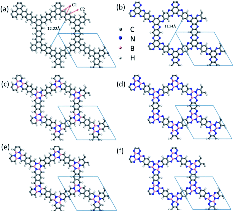 | ||
| Fig. 1 Atomic structures of 2D (a) benzo-CMP, (b) aza-CMP, (c) cis-BN-benzo-CMP, (d) cis-BN-aza-CMP, (e) trans-BN-benzo-CMP and (f) trans-BN-aza-CMP sheets in a 2 × 2 supercell. The rhombus in (a)–(f) represents the unit cell. The gray, white, blue and pink balls denote C, H, N and B atoms, respectively. | ||
Note that the hexagonal boron nitride (h-BN) monolayer has a 2D structure similar to the graphene and their lattice constant difference is only 2%. The h-BN monolayer is an insulator with a wide bandgap of ∼5.9 eV. Recently, planar graphene/h-BN heterostructures or hybrid graphene/h-BN domains have been fabricated as atomically thin integrated circuitry for electronic and optical applications.23–25 Our previous theoretical studies suggest that hybrid graphene/boron nitride nanoribbons can exhibit half-metallicity.26,27 Therefore, either BN co-doping or graphene/h-BN hybridization can be utilized to tune the electronic and transport properties of pure graphene and GNRs.23–27 In this article, we present computed electronic and transport properties of several porous graphene heterostructures, including 2D benzo-CMP and aza-CMP sheets as well as their BN co-doped derivatives (i.e., replacing C1 atoms in hexagonal rings by hexagonal BN rings; see Fig. 1).
Computational details
Geometry optimizations and electronic structure calculations are based on density functional theory (DFT) methods implemented in the SIESTA package.28 The generalized gradient approximation (GGA) in the Perdue–Burke–Ernzerhof (PBE) form is used to treat the exchange-correlation potential29 and the double-ζ polarized numerical atomic-orbital basis sets are selected for the DFT calculations. A real-space grid with an equivalent energy cutoff of 300 Ry is adopted to expand the electron density for numerical integration. The conjugate-gradient method is used to optimize the geometry and all the atoms in the unit cell are fully relaxed until the force on each atom becomes less than 0.01 eV Å−1. A vacuum layer larger than 10 Å is used to avoid interaction among periodic images. The Brillouin zone is sampled at 50 × 50 × 1 Monkhorst meshes. The electron transport properties are computed using the non-equilibrium Green's function (NEGF) method based on the Keldysh formalism, as implemented in the TranSIESTA program.30 The left and right electrodes are chosen to be the same as the scattering region. The current through the system is calculated according to the Landauer–Büttiker formula31| I = G0∫T(E, Vb)[fL(E) − fR(E)]dE |
Results and discussion
Geometrical structures and electronic properties of benzo-CMP and aza-CMP
We first examine the atomic structures of 2D benzo-CMP and aza-CMP, as shown in Fig. 1(a) and (b). Compared with the graphene whose unit cell contains two carbon atoms, the unit cell of 2D benzo-CMP can be constructed by replacing each double bond in the graphene with five fused-benzenes to form a planar graphene-like honeycomb structure, resulting in a wider pore diameter (12.22 Å) compared to that of the 2D polyphenylene (2.48 Å).14 The optimized lattice parameter is 17.27 Å. As shown in Fig. 1(a), there are two different carbon sites in benzo-CMP: each C1 atom is bonded with three carbon atoms and each C2 atom is bonded with two carbon atoms and one hydrogen atom. The bond length of C1–C1 (1.47 Å) is longer than that of C1–C2 (1.40 Å). Obviously, aza-CMP can be constructed by substituting some C2 by N atoms to form N-doped porous graphene, as shown in Fig. 1(b). The optimized lattice constant is 16.59 Å, which is smaller than that of benzo-CMP. The calculated diameter of the pores is 11.54 Å, within the range of experimental values (0.9–1.65 nm).22 Replacing C2 by N makes C1–N (1.327 Å) bond shorter than C1–C2 bond in benzo-CMP. So the pore diameter of aza-CMP is slightly smaller.Next, we compute the electronic properties of benzo-CMP and aza-CMP. The electronic band structure of benzo-CMP is plotted in Fig. 2(a), together with the density of states (DOS). In contrast to the graphene, benzo-CMP is a semiconductor with a direct bandgap of 0.92 eV at the Γ point. This bandgap is less than the bandgap of a polyphenylene network (∼2.35 eV).13–15 Note however that since the PBE/DFT calculation tends to underestimate the bandgap of semiconductors, the realistic bandgap of benzo-CMP may be somewhat larger than 0.92 eV. A partial density of states (PDOS) analysis shows that both C1 and C2 atoms in benzo-CMP contribute to the valence band maximum (VBM) and the conduction band minimum (CBM), and the contribution from C2 atoms is more pronounced than that from C1 atoms. The wavefunctions corresponding to the VBM and CBM states are plotted in the insets of Fig. 2(a). Blue and yellow iso-surfaces represent positive and negative signs of the wavefunction, respectively. It can be seen that the VBM of benzo-CMP is mainly contributed by the pz atomic orbitals of C2 atoms and the sp2 orbitals of C1–C2 bonds, whereas the CBM of benzo-CMP is mainly contributed by the pz atomic orbitals of C2 atoms and the π orbitals of C1 hexagonal rings. Such highly localized states for benzo-CMP are very different from the delocalized π and π* states for the graphene sheet, which lead to semiconducting characteristics for benzo-CMP. For comparison, the electronic band structures and DOS of aza-CMP are shown in Fig. 2(b). Clearly, the aza-CMP is also a semiconductor with a direct bandgap of 1.07 eV, which is slightly larger than that of the benzo-CMP (0.92 eV). Because the number of valence electrons of the nitrogen atom is one more than that of the carbon atom, the N substitution changes the original band filling, shifts the Fermi level upward to the valence band, and induces new electronic states within the valence bands (indicated by red arrows in Fig. 2(b)). Again, to obtain more detailed information about the characteristic semiconducting bands, the amplitude of the wavefunctions of the VBM and CBM are plotted in Fig. 2(b). Clearly, the states corresponding to the CBM of aza-CMP are mainly contributed by the pz atomic orbitals of C2 and N atoms and the π orbitals of C1 hexagonal rings, whereas the states of the VBM of aza-CMP are mainly contributed by the sp2 orbitals of C1–N and C1–C2 bonds, suggesting that the impurity states around the Fermi level due to N atoms are strongly hybridized with the states of C atoms.
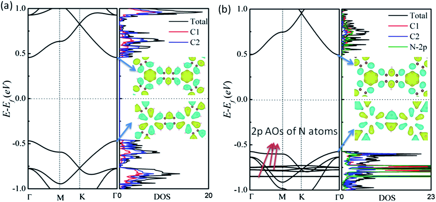 | ||
| Fig. 2 Computed band structures (left panel) and total density of states and partial density of states (right panel) of (a) benzo-CMP and (b) aza-CMP in their primitive unit cell. The wavefunctions of the lowest conduction band and the highest valence band are plotted in the insets, where the isosurface value is 0.05 e Å−3. | ||
Geometrical structures and electronic properties of BN co-doped derivatives
To explore the effect of BN doping on the structures and electronic properties of both benzo-CMP and aza-CMP, we examine several BN co-doped derivatives of benzo-CMP and aza-CMP. Here we use two hexagonal BN rings to replace C1 hexagonal rings in the unit cell. Due to different positions for B and N atoms on the two h-BN rings, four derivatives of the benzo-CMP and aza-CMP, namely, cis-BN-benzo-CMP, cis-BN-aza-CMP, trans-BN-benzo-CMP and trans-BN-aza-CMP, can be constructed, as shown in Fig. 1(c)–(f), respectively. Geometry optimizations show that their unit-cell lattice constant is 17.33 Å, 16.68 Å, 17.36 Å and 16.70 Å, respectively, which is slightly larger than the corresponding lattice constant of benzo-CMP (17.27 Å) or aza-CMP (16.59 Å) because the B–N bond length (1.499 or 1.481 Å) in the h-BN rings is longer than the C1–C1 bond (1.470 Å) in C1 hexagonal rings. Compared to the cis-BN co-doped derivatives with the trans-BN co-doped derivatives, hexagonal pores of the cis-BN-benzo-CMP and cis-BN-aza-CMP appear to be distorted. Electronegativity of C is lower than that of N and greater than that of B, so that the bond length of B–C2 is longer than that of N–C2. Indeed, the bond length of B–C2 and N–C2 in cis-BN-benzo-CMP is 1.492 and 1.352 Å, respectively. When two h-BN rings in the unit cell are arranged according to the cis-position, the difference in bond length results in distorted hexagonal pores. The same situation occurs in cis-BN-aza-CMP.The computed electronic band structures of the four different BN co-doped derivatives are shown in Fig. 3(a)–(d), respectively. It is obvious that BN co-doping plays an important role in tuning the bandgap of benzo-CMP and aza-CMP. They all display distinct semiconducting behaviors. Compared to benzo-CMP and aza-CMP, all four derivatives possess smaller bandgaps. In details, trans-BN-benzo-CMP has a direct bandgap of 0.57 eV, nearly the same as that of cis-BN-benzo-CMP (0.58 eV), while trans-BN-aza-CMP has the smallest bandgap with the value of 0.47 eV, notably less than that of cis-BN-aza-CMP (0.6 eV).
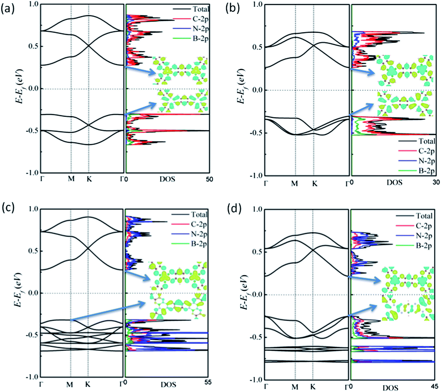 | ||
| Fig. 3 Computed band structures and total density of states and partial density of states of BN co-doped derivatives: (a) cis-BN-benzo-CMP, (b) trans-BN-benzo-CMP, (c) cis-BN-aza-CMP and (d) trans-BN-aza-CMP. The wavefunctions of the lowest conduction band and the highest valence band are plotted in the insets, where the isosurface value is 0.05 e Å−3. | ||
To clarify the influence of BN co-doping, the total density of states (TDOS) and PDOS of the four derivatives are shown in Fig. 3(a)–(d), respectively. For trans-BN-benzo-CMP and cis-BN-benzo-CMP, there is a peak at the bottom of the conduction band in PDOS of N and C atoms and a peak at the top of the valence band in PDOS of B and C atoms, which means that the N atoms mainly contribute to the bottom of the conduction band and B atoms mainly contribute to the top of valence band, consistent with the wavefunction distribution of the VBM and CBM shown in the insets of Fig. 3(a) and (b), respectively. Here one can see that the VBM is mainly contributed by the pz atomic orbitals of C2 atoms and the sp2 orbitals of B–C2 bonds, whereas the CBM is mainly contributed by the pz atomic orbitals of C2 atoms and the delocalized π orbitals of N atoms. It is known that the 2s- and the 2p-electronic orbital energies of C atoms are higher than those of N atoms but lower than those of B atoms. Therefore, the doping of B atoms will move the corresponding energy bands upward and the doping of N atoms will move the energy bands downward. As the VBM is mainly contributed by B atoms and the CBM is contributed by N atoms for trans-BN-benzo-CMP and cis-BN-benzo-CMP, as a result, the bottom of the conduction band moves downward and the top of the valence band moves upward, resulting in reduced bandgap in comparison with benzo-CMP. h-BN co-doping shows a similar influence for trans-BN-aza-CMP and cis-BN-aza-CMP. As shown in the total DOS and PDOS in Fig. 3(c) and (d), N atoms mainly contribute to the bottom of the conduction band and both B and N atoms contribute to the top of the valence band, consistent with the wavefunction distribution of the VBM and CBM shown in the insets of Fig. 3(c) and (d). From the wavefunction distribution of the VBM and CBM one can find that B atom contributions on h-BN rings to the top of the valence band are larger than the corresponding N atom contributions. Thus the influence of the B atoms shifts up the VBM and N atoms shifts down the CBM, which results in the reduced bandgap of trans-BN-aza-CMP and cis-BN-aza-CMP, compared to aza-CMP.
Transport properties
In addition to the electronic structures, we compute the electron transport properties and current–voltage (I–Vb) characteristics of the benzo-CMP and aza-CMP and their BN co-doped derivatives. A two-probe system is employed to compute the I–Vb curve. Here, we treat the trans-BN-aza-CMP as a prototype model for the discussion. As shown in Fig. 4(a), the semi-infinite left- and right-electrodes are in contact with a finite central scattering region with the same width. Both electrodes and the central region are made of the 2D trans-BN-aza-CMP sheet. The transmissions are in the z axis direction. Periodic boundary conditions are imposed on the plane normal to the z direction. The computed zero-bias transmission spectrum is shown in Fig. 4(b), which apparently mimics the band structure of the trans-BN-aza-CMP sheet. There is a region of zero transmission with a width of 0.49 eV located around the Fermi level, coinciding with the computed bandgap (0.47 eV) of the trans-BN-aza-CMP sheet. The current versus bias voltage curve is shown in Fig. 4(c), which displays typical semiconducting behavior, consistent with the zero-bias transmission spectrum shown in Fig. 4(b). The system exhibits a threshold voltage Vth = 0.6 V below which the current is nearly zero. | ||
| Fig. 4 (a) Schematic view of the two-probe trans-BN-aza-CMP device. (b) Computed transmission spectra of benzo-CMP, aza-CMP, cis-BN-benzo-CMP, trans-BN-benzo-CMP, cis-BN-aza-CMP and trans-BN-aza-CMP under zero bias voltage, respectively. (c) Variation of current as a function of the bias voltage (I–Vb curves). | ||
To further understand the semiconducting I–Vb characteristic of the 2D trans-BN-aza-CMP sheet, the transmission spectra at two typical bias voltages are presented in Fig. 5(a). It is known that the current is mainly attributed to the transmission coefficient around the Fermi level within the bias window. At zero bias, there is a transmission gap of 0.49 eV due to the bandgap of trans-BN-aza-CMP. When the bias is increased to Vth = 0.6 V, the valence band of the left electrode matches well with the bottom of the conduction band of the right electrode, as shown in Fig. 5(b). Consequently, the electrons can tunnel from the valence band of the left electrode to the conduction band of the right one, resulting in a transmission peak around the Fermi level within the bias window. Based on the Landauer–Büttiker formula, the current should flow. Compared with the case of 0.6 V bias, when the bias window widens from [−0.3, 0.3] V to [−0.5, 0.5] V under the bias of 1.0 V, the transmission coefficient becomes larger, leading to a notable increase in the current.
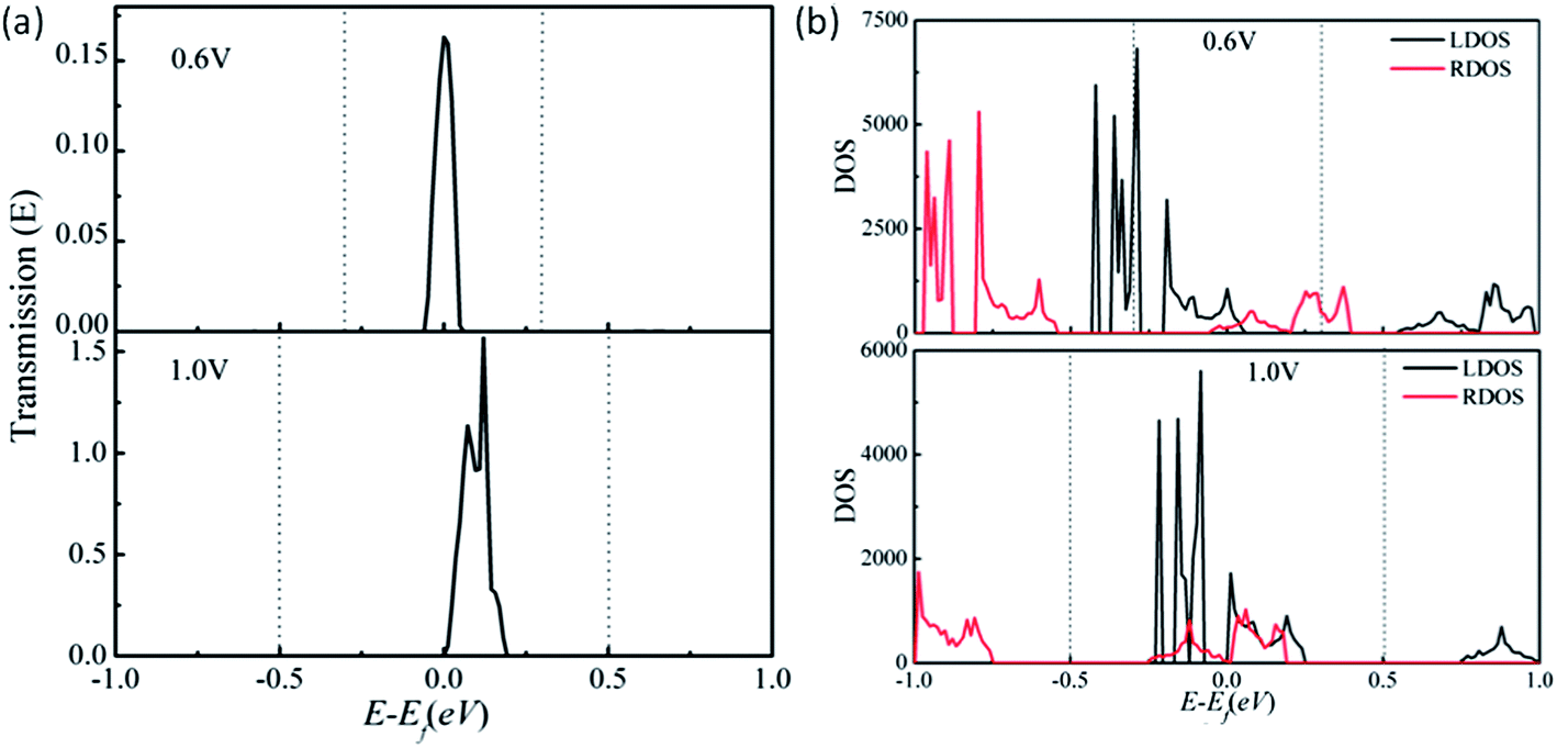 | ||
| Fig. 5 (a) Computed transmission spectra of trans-BN-aza-CMP for 0.6 and 1.0 V bias voltages, respectively. The dashed lines indicate the bias windows. (b) Density of states of the left (LDOS) and right (RDOS) electrodes under the 0.6 and 1.0 V bias voltages for the two-probe trans-BN-aza-CMP device. | ||
For comparison, the I–Vb curves of benzo-CMP, aza-CMP, cis-BN-benzo-CMP, trans-BN-benzo-CMP and cis-BN-aza-CMP at zero bias are presented in Fig. 4(c). As mentioned above, the benzo-CMP and aza-CMP are semiconductors with a direct bandgap of 0.92 and 1.07 eV, respectively. So, the current cannot be observed until the bias voltage exceeds 1.0 V for benzo-CMP. But the current does not arise even when the bias voltage reaches 1.2 V for aza-CMP. On the other hand, due to the smaller bandgaps for all the BN co-doped derivatives, smaller transmission gaps at zero bias voltage, i.e., 0.58, 0.58, 0.63 and 0.49 eV, are found for cis-BN-benzo-CMP, trans-BN-benzo-CMP, cis-BN-aza-CMP and trans-BN-aza-CMP, respectively, consistent with their corresponding band structures. When the bias is greater than Vth, the current arises. More specifically, obvious current is seen when the bias is greater than 0.6 V for trans-BN-benzo-CMP. Moreover, the transmission coefficient increases with increasing the bias voltage in the range of 0.6–1.0 V, which leads to the monotonic current increase in this bias window, similar to trans-BN-aza-CMP. For cis-BN-benzo-CMP and cis-BN-aza-CMP, the current also starts to arise when the bias exceeds 0.6 V. However, the current becomes constant (∼1.0 μA) from 0.6 to 1.0 V, consistent with the transmission spectra shown in Fig. S1 in the ESI.†
Conclusion
In conclusion, we have shown that 2D benzo-CMP and aza-CMP sheets and their BN co-doped derivatives possess distinct structural, electronic and transport properties that are notably different from those of graphene. Our DFT computations show that the benzo-CMP and aza-CMP, both being porous graphenes with a relatively large pore size, are semiconductors with a direct bandgap of 0.92 and 1.07 eV, respectively. The computed I–Vb curves are consistent with of the semiconducting characteristics. BN co-doped derivatives possess relatively small bandgaps (0.47–0.6 eV). The tunable electronic and transport properties of benzo-CMP and aza-CMP through BN co-doped derivatives may be exploited for applications in low-dimensional nanoelectronic devices.Acknowledgements
We are grateful to Professor Jian Zhang for valuable discussions. This work is supported by NSF (DMR-0820521), ARL (W911NF1020099), the Nebraska Research Initiative, the UNL Nebraska Center for Energy Sciences Research, UNL Holland Computing Center, and a grant from USTC for (1000plan) Qianren-B summer research.References
- K. S. Novoselov, A. K. Geim, S. V. Morozov, D. Jiang, Y. Zhang, S. V. Dubonos, I. V. Grigorieva and A. A. Firsov, Science, 2004, 306, 666–669 CrossRef CAS PubMed.
- A. K. Geim, Science, 2009, 324, 1530–1534 CrossRef CAS PubMed.
- A. H. Castro Neto, F. Guinea, N. M. R. Peres, K. S. Novoselov and A. K. Geim, Rev. Mod. Phys., 2009, 81, 109–162 CrossRef CAS.
- F. Bonaccorso, Z. Sun, T. Hasan and A. C. Ferrari, Nat. Photonics, 2010, 4, 611–622 CrossRef CAS.
- C. Berger, Z. Song, X. Li, X. Wu, N. Brown, C. Naud, D. Mayou, T. Li, J. Haas, A. N. Marchenkov, E. H. Conrad, P. N. First and W. A. de Heer, Science, 2006, 312, 1191–1196 CrossRef CAS PubMed.
- G. Brumfiel, Nature, 2009, 458, 390–391 CrossRef CAS PubMed.
- Y. An, X. Wei and Z. Yang, Phys. Chem. Chem. Phys., 2012, 14, 15802–15806 RSC.
- L. Kou, C. Tang, C. Chen and W. Guo, J. Appl. Physiol., 2011, 110, 124312 CrossRef PubMed.
- Y. Li, Z. Zhou, P. Shen and Z. Chen, ACS Nano, 2009, 3, 1952–1958 CrossRef CAS PubMed.
- X.-F. Li, L.-L. Wang, K.-Q. Chen and Y. Luo, J. Phys.: Condens. Matter, 2012, 24, 095801 CrossRef PubMed.
- M. Bieri, M. Treier, J. M. Cai, K. Ait-Mansour, P. Ruffieus, O. Groning, P. Groning, M. Kastler, R. Rieger, X. L. Feng, K. Mullen and R. Fasel, Chem. Commun., 2009, 45, 6919–6921 RSC.
- A. Du, Z. Zhu and S. C. Smith, J. Am. Chem. Soc., 2010, 132, 2876–2877 CrossRef CAS PubMed.
- M. Hatanaka, Chem. Phys. Lett., 2010, 488, 187–192 CrossRef CAS PubMed.
- Y. Li, Z. Zhou, P. Shen and Z. Chen, Chem. Commun., 2010, 46, 3672–3674 RSC.
- Y. Ding, Y. Wang, S. Shi and W. Tang, J. Phys. Chem. C, 2011, 115, 5334–5343 CAS.
- A. I. Cooper, Adv. Mater., 2009, 21, 1291–1295 CrossRef CAS.
- A. Thomas, Angew. Chem., Int. Ed., 2010, 49, 8328–8344 CrossRef CAS PubMed.
- X. Han, L. Li, Z. Huang, J. Liu and Q. Zheng, Chin. J. Chem., 2013, 31, 617–623 CrossRef CAS.
- X. Feng, Y. Liang, L. Zhi, A. Thomas, D. Wu, I. Lieberwirth, U. Kolb and K. Müllen, Adv. Funct. Mater., 2009, 19, 2125–2129 CrossRef CAS.
- L. Chen, Y. Honsho, S. Seki and D. Jiang, J. Am. Chem. Soc., 2010, 132, 6742–6748 CrossRef CAS PubMed.
- M. Hatanaka, J. Phys. Chem. C, 2012, 116, 20109–20120 CAS.
- Y. Kou, Y. Xu, Z. Guo and D. Jiang, Angew. Chem., Int. Ed., 2011, 50, 8753–8757 CrossRef CAS PubMed.
- Z. Liu, L. Ma, G. Shi, W. Zhou, Y. Gong, S. Lei, X. Yang, J. Zhang, J. Yu, K. P. Hackenberg, A. Babakhani, J.-C. Idrobo, R. Vajtai, J. Lou and P. M. Ajayan, Nat. Nanotechnol., 2013, 8, 119–124 CrossRef CAS PubMed.
- Y. Gao, Y. Zhang, P. Chen, Y. Li, M. Liu, T. Gao, D. Ma, Y. Chen, Z. Cheng, X. Qiu, W. Duan and Z. Liu, Nano Lett., 2013, 13, 3439–3443 CrossRef CAS PubMed.
- M. P. Levendorf, C.-J. Kim, L. Brown, P. Y. Huang, R. W. Havener, D. A. Muller and J. Park, Nature, 2012, 488, 627–632 CrossRef CAS PubMed.
- E.-J. Kan, X. Wu, Z. Li, X. C. Zeng, J. Yang and J. G. Hou, J. Chem. Phys., 2008, 129, 084712 CrossRef PubMed.
- Y. Liu, X. Wu, Y. Zhao, X. C. Zeng and J. Yang, J. Phys. Chem. C, 2011, 115, 9442–9450 CAS.
- J. M. Soler, E. Artacho, J. D. Gale, A. García, J. Junquera, P. Ordejón and D. Sánchez-Portal, J. Phys.: Condens. Matter, 2002, 14, 2745–2779 CrossRef CAS.
- J. P. Perdew, K. Burke and M. Ernzerhof, Phys. Rev. Lett., 1996, 77, 3865–3868 CrossRef CAS.
- M. Brandbyge, J. L. Mozos, P. Ordejón, J. Taylor and K. Stokbro, Phys. Rev. B: Condens. Matter Mater. Phys., 2002, 65, 165401 CrossRef.
- M. Büttiker, Y. Imry, R. Landauer and S. Pinhas, Phys. Rev. B: Condens. Matter Mater. Phys., 1985, 31, 6207–6215 CrossRef.
- A. Garcia-Lekue and L. W. Wang, Phys. Rev. B: Condens. Matter Mater. Phys., 2010, 82, 035410 CrossRef.
Footnote |
| † Electronic supplementary information (ESI) available: Computed transmission spectra and the corresponding DOS of the left electrode and the right electrode at different biases for (a) benzo-CMP, (b) aza-CMP, (c) cis-BN-benzo-CMP, (d) trans-BN-benzo-CMP, and (e) cis-BN-aza-CMP. See DOI: 10.1039/c3tc32363c |
| This journal is © The Royal Society of Chemistry 2014 |