 Open Access Article
 This Open Access Article is licensed under a
 Creative Commons Attribution 3.0 Unported Licence
Chemically amplified phenolic fullerene electron beam resist†
D. X.
Yang
ab,
A.
Frommhold
a,
X.
Xue
c,
R. E.
Palmer
b and
A. P. G.
Robinson
*a
aSchool of Chemical Engineering, University of Birmingham, Edgbaston, Birmingham, B15 2TT, UK. E-mail: a.p.g.robinson@bham.ac.uk
bNanoscale Physics Research Laboratory, School of Physics and Astronomy, University of Birmingham, Edgbaston, Birmingham, B15 2TT, UK
cNano-C Inc., 33 Southwest Park, Westwood, MA 02090, USA
First published on 18th December 2013
Abstract
Molecular resist materials for electron beam lithography have received significant interest as a route to reducing line width roughness and improving resolution. However, they have often required the use of hazardous solvents in their processing. A new family of fullerene based negative tone chemically amplified e-beam resists, using industry compatible solvents, has been developed. A sensitivity of ∼40 μC cm−2 was achieved at 20 keV. Isolated features with a line width of 13.6 nm as well as ∼20 nm lines on a 36 nm pitch have been patterned, whilst one variant has demonstrated resolution to 15 nm half-pitch at slightly higher dose.
Introduction
Since the invention and commercialization of the integrated circuit in the 1960s, the semiconductor industry has unremittingly sought to achieve increasingly complex circuits in smaller areas.1,2 This has led to the requirement for continuous shrinkage of the minimum lithographic feature size. The International Technology Roadmap for Semiconductors (ITRS)3 has specified 20 nm DRAM half-pitch (hp) and 14 nm Flash half-pitch as target resist requirements for 2016. Whilst it has been possible to extend current 193 nm photolithography far beyond expectation, to allow sub-30 nm patterning,4,5 this has been at the cost of greatly increased complexity of the patterning or post-exposure processing,6 which dramatically impacts yield and cost. Electron-beam lithography (EBL), traditionally considered to be high-resolution but slow, has primarily found application in the semiconductor industry for the fabrication of reticles.7 However, as resolution requirements have increased there has been increasing focus on EBL for volume production, with the development of a number of multi-beam and hybrid technologies.8–11 Due to the low-throughput, even for multi-beam EBL, the sensitivity of e-beam resists is considered a very important factor. For high voltage e-beam exposure, a 50–60 μC cm−2 resist sensitivity requirement has been set out by ITRS, whilst low voltage systems, such as MAPPER,11 require sensitivities of 30–60 μC cm−2.3It is well known that sub-20 nm resolution can be achieved in positive tone EBL resists. Poly(methyl methacrylate) (PMMA; various suppliers) has sub-10 nm sparse feature resolution with 30 keV electrons using standard developer at low temperature (4 °C),12 and 16 nm half-pitch using 80 keV electrons and an unconventional developer13 but in both cases requires a relatively high exposure dose (400 and 1200 μC cm−2 respectively). The ZEP series of resists (ZEP-520A, 7000; Nippon Zeon) have demonstrated both sub-20 nm dense feature resolution and high sensitivity, but not simultaneously (e.g. 40 nm half-pitch with 5 keV electrons and a dose of 2.6 μC cm−2;14 or 12 nm half-pitch at 25 keV with a dose of 300 μC cm−2).15
For negative tone resists the situation is worse – with high resolution resists typically requiring huge doses and fast resists failing to achieve high resolution. Hydrogen silsesqioaxene (HSQ) has amongst the highest dense feature resolution of any resist to date – sub-5 nm half-pitch.16 However the dose required is extremely poor (5000 pC cm−1 line dose at 10 keV;16 area dose of 2500–3000 μC cm−2 at 100 keV).17 Likewise, calixarene,18 negative tone PMMA,19 and polystyrene20 achieve impressive resolution whilst sacrificing speed.
For high-sensitivity negative tone commercial resists such as SU-8 (MicroChem) and AZnLOF 2020 (AZ Electronic Materials) the minimum resolved dense features reported thus far are 70 nm half-pitch21 and 50 nm half-pitch22 respectively. A non-commercial epoxy based negative tone high speed resist with 25 nm half-pitch resolution at 38 μC cm−2 sensitivity (at 100 keV) has demonstrated.21
Chemical amplification (CA), in which a catalytic reaction process is used to amplify the effect of each quantum of radiation, is an efficient approach to enhance resist sensitivity and thus throughput.23,24 The major issue for chemically amplified resists (CAR) is to simultaneously satisfy the manufacturing requirements for resolution, line width roughness, and sensitivity (RLS). Although the factors determining the RLS trade-off relationship are still under investigation,25,26 it has been shown that CARs based on molecular27,28 rather than polymeric resists have the potential for lower line width roughness (LWR)29 and higher resolution while maintaining good sensitivity. We have previously developed a series of chemically amplified e-beam resists based on fullerene derivatives containing polyethyleneglycol side chains,30,31 which have shown high sensitivity, high resolution, good LWR and excellent etch durability.32 However, in common with several other negative tone molecular resist materials33–35 it was necessary to use halogenated solvents for spin coating and development that were not acceptable (safe) for commercial use.
In this study we present a new family of phenol based fullerene derivatives, (Irresistible Materials Ltd) including a phenolic methanofullerene IM-MFP12-3 and a tert-butoxycarbonyl (tBOC) group protected derivative IM-MFPT12-2, as well as a longer side-chain version IM-MFPT12-8 (Fig. 1a). These materials are compatible with industry-friendly casting solvents – such as propylene glycol monomethyl ether (PGME) and ethyl lactate, – and developers, such as cyclohexanone, 2-heptanone and n-butyl acetate. The ability to use industrially approved solvents is critical for commercial acceptance. The tBOC protected fullerene derivatives were designed to work as a positive tone CAR by acid induced deprotection of the tBOC labile groups,36,37 but were also found to have excellent negative tone performance when combined with an epoxy crosslinker (shown in Fig. 1b, from Huntsman Advanced Materials) and triphenylsulfonium hexafluoroantimonate (Fig. 1c, from Midori Kagaku Co.) as photo-acid generator (PAG).38
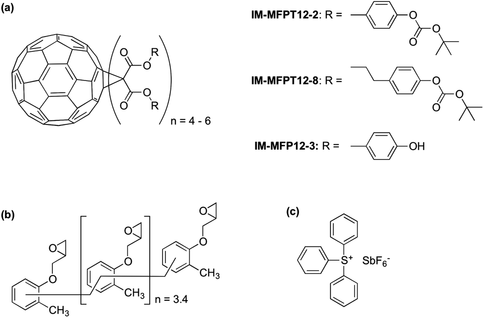 | ||
| Fig. 1 Resists were formulated from (a) IM-MFPT12-2 – a tert-butoxycarbonyl (tBOC) protected phenolic malonate C60; IM-MFPT12-8 – a tBOC protected propyl phenolic malonate C60; and IM-MFP12-3 – a phenolic malonate C60, (b) epoxy crosslinker, and (c) triphenylsulfonium hexafluoroantimonate photoacid generator. | ||
Experimental
Synthesis of fullerene derivatives
Synthesis of the IM-MFPT12-2, IM-MFPT12-8 and IM-MFP12-3, was achieved via the modified Bingel39,40 cyclopropanation reaction of a bismalonate ester, with the C60, to afford the methanofullerenes. The product of the reaction was purified by flash chromatography on silica gel. The expected structure was confirmed by mass spectrometry. All the reactions were carried out under a nitrogen atmosphere. Chemicals were purchased from Aldrich and used as received. Yields refer to chromatographically pure products. Thin-Layer Chromatography (TLC) was carried out on aluminum sheets coated with silica gel 60 (Merck 5554 mesh). Column chromatography was performed on silica gel 60 (Merck 230-400).IM-MFPT12-2 (Scheme 1): to a 250 mL round bottom flask was added 4-hydroxybenzyl alcohol (12.4 g, 100 mmol), dichloromethane (100 mL) and di-tert-butyldicarbonate (21.8 g, 100 mmol). The mixture was cooled to 0 °C in an ice bath. Potassium carbonate (37 g, 268 mmol) and 18-crown-6 (1.32 g, 5 mmol) dissolved in dichloromethane were added. The resulting mixture was stirred and warmed to room temperature overnight. The crude reaction mixture was filtered through a silica gel plug in a sintered glass funnel and rinsed with ethyl acetate. The resulting solvent was evaporated and the residue was purified via flash column chromatography on silica gel with ethyl acetate–hexane (40%) as eluent. The third fraction was combined and the solvent removed to give 9.8 g (yield: 45%) of 4-(t-butoxycarbonyl)benzyl alcohol 1 as a yellow oil. δH (300 MHz, CDCl3) 1.57 (9 H, s, CH3), 4.56 (2 H, s, CH2), 7.13 (2 H, d, ArH) and 7.32 (2 H, d, ArH). Dichloromethane (50 mL) was added to 1 (2.24 g, 10 mmol) in a 250 mL round bottom flask. To this was added, with stirring, pyridine (1.05 g, 13.3 mmol, 1.33 equiv.) and the solution was cooled to 0 °C in an ice bath. Malonyl dichloride (0.49 mL, 5 mmol, in DCM solution) was added dropwise. The initially clear solution became dark red upon complete addition of the malonyl dichloride. The mixture was stirred and warmed up to room temperature overnight, after which it was dark blue/green in color. The mixture was filtered through a silica gel plug and rinsed through with ethyl acetate. The filtrate was evaporated and the residue was purified via flash column chromatography on silica gel using ethyl acetate as eluent. The fractions were collected and solvent removed to give the t-butoxycarbonyl malonate 2 as yellow-reddish oil (1.73 g, 34% yield). δH (300 MHz, CDCl3) 1.55 (18 H, s, CH3), 3.44 (2 H, s, CH2), 5.14 (4 H, s, CH2), 7.14 (4 H, d, ArH) and 7.35 (4 H, d, ArH). To 1 L round bottom flask, [60]fullerene (0.85 g, 1.2 mmol), 9,10-dimethylancethracene (2.62 g, 13 mmol, 11 equiv.) and toluene (500 mL) were added. The resulting solution was stirred for one hour to completely dissolve the fullerene. Carbon tetrabromide (4.78 g, 13 mmol, 11 equiv.) and 2 (6.6 g, 13 mmol, equiv.) were added to the solution. DBU (8.3 mL, 53.2 mmol) was added dropwise and the resulting mixture was stirred at room temperature overnight – the initial purple solution had was dark red in color. The crude mixture was poured though a silica gel plug in a sintered glass funnel and rinsed with toluene to remove unreacted [60]fullerene. After that the plug was rinsed with dichloromethane–ethyl acetate–methanol (2![[thin space (1/6-em)]](https://www.rsc.org/images/entities/char_2009.gif) :2:1) to remove the red/brown band containing the crude products. The filtrate was evaporated and the resulting residue was purified via flash column chromatography with dichloromethane–ethyl acetate–methanol as eluent. (t-Butoxycarbonyl malonate)-methano-[60]fullerene: 3 (1.8 g, dark red/brown oil) was obtained.
:2:1) to remove the red/brown band containing the crude products. The filtrate was evaporated and the resulting residue was purified via flash column chromatography with dichloromethane–ethyl acetate–methanol as eluent. (t-Butoxycarbonyl malonate)-methano-[60]fullerene: 3 (1.8 g, dark red/brown oil) was obtained.
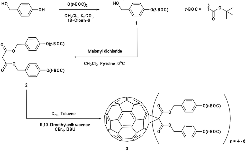 | ||
| Scheme 1 Synthesis of (t-butoxycarbonyl malonate)-methano-[60]fullerene (IM-MFPT12-2). | ||
IM-MFPT12-8 (Scheme 2): to a 250 mL round bottom flask was added 3-(4-hydroxyphenyl)-1-propanol (10 g, 65.7 mmol), dichloromethane (75 mL) and di-tert-butyldicarbonate (14.36 g, 65.7 mmol). The mixture was stirred and cooled to 0 °C in an ice bath. Potassium carbonate (24.37 g, 176 mmol) and 18-crown-6 (0.90 g, 3.4 mmol) dissolved in dichloromethane were added. The resulting mixture was stirred and warmed to room temperature overnight. The crude reaction mixture was filtered through a silica gel and rinsed with ethyl acetate. The resulting solvent was evaporated and the residue was purified via flash column chromatography on silica gel with ethyl acetate–hexane (40%) as eluent. The third fraction was combined and the solvent removed to give 15.7 g (yield: 95%) of 3-(4-t-butoxycarbonyl)phenyl-1-propanol 4 as a yellow oil. δH (300 MHz, CDCl3) 1.55 (9 H, s, CH3), 1.87 (2 H, m, CH2), 2.69 (2 H, t, CH2), 3.65 (2 H, t, CH2), 5.29 (1 H, s, OH), 7.06 (2 H, d, ArH) and 7.19 (2 H, d, ArH). Dichloromethane (275 mL) was added to 4 (13.71 g, 54.4 mmol) in a 500 mL round bottom flask. To this was added, with stirring, pyridine (5.72 g, 72.35 mmol, 1.33 equiv.) and the solution was cooled to 0 °C in an ice bath. Malonyl dichloride (2.65 mL, 27.2 mmol, in dichloromethane solution) was added dropwise. The initially clear solution became dark red upon complete addition of the malonyl dichloride. The mixture was stirred and warmed to room temperature overnight, after time it became dark blue/green in color. The mixture was filtered through silica gel with ethyl acetate. The filtrate was evaporated and the residue was purified via flash column chromatography on silica gel using ethyl acetate as eluent. The fractions were collected and solvent removed to give 3-(4-t-butoxycarbonyl)phenyl-1-propyl malonate 5 as yellow oil (9.56 g, 61% yield). δH (300 MHz, CDCl3) 1.55 (18 H, s, CH3), 1.86 (4 H, m, CH2), 2.69 (4 H, m, CH2), 3.66 (4 H, m, CH2), 7.07 (4 H, d, ArH) and 7.17 (4 H, d, ArH). In a round bottom flask, [60]fullerene (1 equiv.), 9,10-dimethylancethracene (22 equiv.) and toluene were added. The resulting solution was stirred for one hour to completely dissolve the fullerene. Carbon tetrabromide (22 equiv.) and 5 (22 equiv.) were added to the solution. 1,8-Diazabicyclo[5.4.0]undec-7-ene (108 equiv.) was added dropwise and the resulting mixture was stirred at room temperature overnight after which the initial purple solution was a dark red color. The crude mixture was poured though silica gel with toluene to remove unreacted [60]fullerene, and then rinsed with dichloromethane–ethyl acetate–methanol (2:2:1) to remove the red/brown band containing the crude products. The solvents were evaporated and the resulting residue [3-(4-t-butoxycarbonyl)phenyl-1-propyl malonate]-methano-[60]fullerene 6 (dark red/brown oil) was obtained. δH (300 MHz, CDCl3) 1.55 (s, CH3), 0.9–4.1 (m, CH2), 6.90–7.70 (m, ArH).
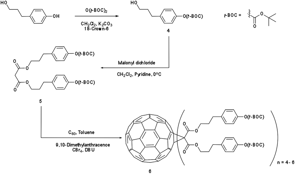 | ||
| Scheme 2 Synthesis of [3-(4-t-butoxycarbonyl)phenyl-1-propyl malonate]-methano-[60]fullerene (IM-MFPT12-8). | ||
IM-MFP12-3 (Scheme 3): in a 50 mL round bottom flask, 3 was dissolved in dichloromethane (10 mL) and stirred under nitrogen. Triflic acid (0.1 mol%) was added and stirred for 4 hours. The solvent was removed under vacuum and the resulting residue (3-phenol-1-propyl malonate)-methano-[60]fullerene 7 was obtained. δH (300 MHz, CDCl3) 0.9–4.0 (m, CH2), 6.8–7.8 (m, ArH), no singlet at 1.55.
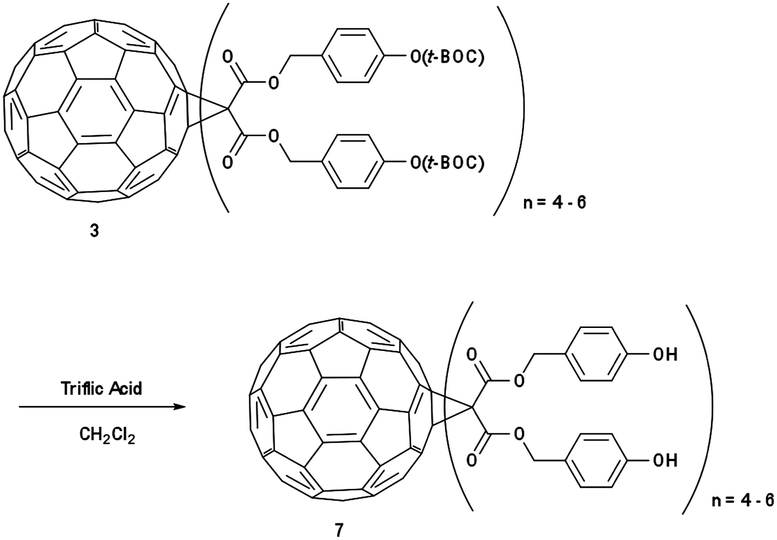 | ||
| Scheme 3 Synthesis of (3-phenol-1-propyl malonate)-methano-[60]fullerene (IM-MFP12-3). | ||
Resist film preparation
Silicon chips diced from a 100 mm wafer (Rockwood Electronic Materials, n-type, 〈100〉) were used as substrates for all of the samples. Chemicals were purchased from Aldrich except where mentioned, and used as received. The substrates were cleaned with a 15 min ultrasonic wash in acetone followed by 15 min in isopropyl alcohol (IPA). The substrates were subsequently dried with nitrogen before spin coating. The fullerene derivative, crosslinker and PAG were each dissolved in PGME with a 10–20 g l−1 concentration. The resist was then formulated by mixing the three solutions to give a ratio of one part fullerene derivative, two parts crosslinker and one part PAG by weight. By adjusting the concentration of the resist solution as well as the spin speed, a 30–50 nm resist film was prepared for sensitivity tests while a 20–30 nm film was spun for high-resolution tests. A 75 °C/5 min post-application bake (PAB) was applied after spin coating.Lithographic evaluation
An FEI XL30 SFEG field emission scanning electron microscope with ELPHY Plus pattern generator (Raith GmbH) was used for e-beam exposures. For sensitivity and contrast evaluation, a beam voltage of 20 keV was used to pattern a set of 75 × 75 μm squares with electron doses ranging from 0.5 μC cm−2 to 500 μC cm−2. The film thickness of each square remaining after development was measured using a surface profiler (Dektak 3st Auto). A sigmoid function was used to fit the response curve to extract the sensitivity (i.e. dose for the 50% remaining film thickness) and contrast (the slope of the linear rising portion of the curve). For all high-resolution tests, a 30 keV acceleration voltage was used with ∼40 pA beam current. Single pixel lines were patterned in these tests and the dosage was described as a line dose (pC cm−1).Various post exposure bake (PEB) conditions were used in this study. Three industry acceptable non-halogenated developers have been evaluated and compared to the monochlorobenzene (MCB) and IPA [1:1] developer used in previous studies. The development conditions were dip development for 20 s followed by a rinse in IPA for several seconds unless otherwise described. The LWR was measured using SuMMIT.
Plasma etching
Silicon etching was performed with an Oxford Instruments PlasmaPro NGP80 tool using inductively coupled plasma (ICP) technology. The gas mixture used was either SF6/CHF3 or SF6/C4F8. The process conditions were 15 sccm SF6, 50 sccm CHF3, 20 W RF power and 200 W ICP power at 15 mT chamber pressure and a temperature of 5 °C. Alternative conditions were 25 sccm SF6, 30 sccm C4F8, 20 W RF power and 220 W ICP power. The resist thickness was measured with the surface profiler prior to etching and remeasured after silicon etching. Afterwards the residual resist was stripped with oxygen plasma and the height of the silicon features measured again. The etch rate of the resist material was then calculated from these measurements.Results and discussions
Sensitivity and contrast evaluation
The response of the resists to electron irradiation was evaluated at 20 keV. Fig. 2a shows the responses of IM-MFP12-3, IM-MFPT12-2 and IM-MFPT12-8 after exposure and development for 20 s in MCB–IPA [1:1]. The sensitivities and contrasts (given in brackets), calculated from the fitted curves, were 32 μC cm−2 (1.0), 93 μC cm−2 (1.8) for IM-MFP12-3 and IM-MFPT12-2, respectively. The crosslinking reaction mechanism of the tBOC protected material IM-MFPT12-2 is still under investigation, but we speculate a two-step reaction in which the tBOC protection group is first removed catalytically by the PAG generated acid, leaving a phenol, which then crosslinks cationically with the epoxy.38,41 The additional deprotection step might result in the lower sensitivity and higher contrast of IM-MFPT12-2 compared with IM-MFP12-3.
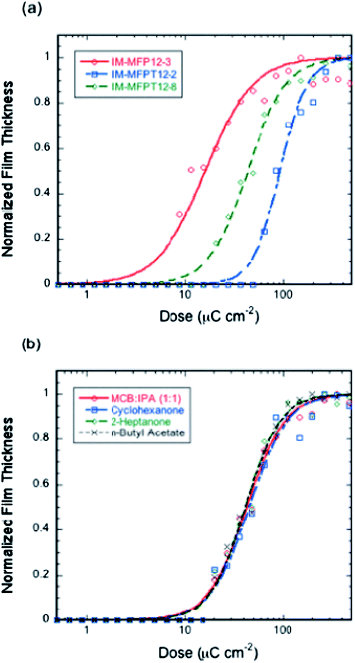 | ||
| Fig. 2 Response curves of (a) IM-MFPT12-2, IM-MFP12-3 and IM-MFPT12-8 resists with 1:2:1 compound ratio of fullerene, crosslinker and photo-acid generator; 75 °C/5 min post-application bake and 90 °C/2 min post-exposure bake; MCB–IPA [1:1] developer, and (b) IM-MFPT12-8 resist developed in MCB–IPA [1:1], cyclohexanone, 2-heptanone, or n-butyl acetate (all other conditions as for (a)). | ||
However, significant improvement of sensitivity was achieved for the tBOC protected material by using a longer side chain – IM-MFPT12-8. The sensitivity and contrast (given in brackets) of IM-MFPT12-8 were 43 μC cm−2 (1.3) as shown in Fig. 2a. The enhanced sensitivity might due to one or more of several effects. The higher flexibility of longer side chain compared with the shorter side chain, might be expected to reduce potential steric hindrance, and has been shown to help improve the crosslinking.42 Moreover, an increased chain length between the bulky side group and the main chain was also reported to improve the sensitivity of some other polymer based resists due to enhanced acid diffusion.43 It has also been shown that for chemically amplified resists exposed via high energy techniques (such as electron beam lithography) the ability of the non-PAG components to be deprotonated can have a large effect on sensitivity.44
In order to evaluate the industrial viability of the resists, a variety of non-halogenated developers have been tested. Fig. 2b shows the responses of IM-MFPT12-8 resist developed in three industrially acceptable negative tone developers – cyclohexanone, 2-heptanone and n-butyl acetate and, for comparison, MCB–IPA. All other process conditions for the four samples were identical. The sensitivity and contrast (in brackets) of the resist with cyclohexanone, 2-heptanone and n-butyl-acetate development were 46 μC cm−2 (1.3), 42 μC cm−2 (1.4), and 42 μC cm−2 (1.4), respectively, showing no significant variation in sensitivity or contrast, thus confirming the compatibility of the new resist with industrially friendly developers and casting solvents.
Etch durability
The etch durability of the resist material was determined by performing blanket etch tests on patterned squares of IM-MFPT12-8 as used for the sensitivity measurements. It was evaluated for both SF6/CHF3 and SF6/C4F8 mixed mode etch chemistries. As a control, Rohm and Haas SAL601, a high-durability novolac-based conventional resist, was etched as well. For SF6/CHF3 chemistry the resist was etched at a rate of 1.21 nm s−1 resulting in 5.64:1 selectivity over silicon while SAL601 had 1.43 nm s−1 etch rate with 4.79:1 selectivity. In SF6/C4F8 the IM-MFPT12-8 etched at 0.97 nm s−1 with 3.53:1 selectivity in contrast to the control, which was removed at a rate of 1.24 nm s−1 with 2.77:1 selectivity. The increase in selectivity between the two gas mixtures is caused by the higher silicon etch rate of the SF6/CHF3 gas mix. Comparing the results of the two materials, the fullerene resist shows a higher etch durability over the SAL601 control, which is attributed to its high degree of unsaturation, and conforms with results in previous fullerene based systems.32
Resolution evaluation
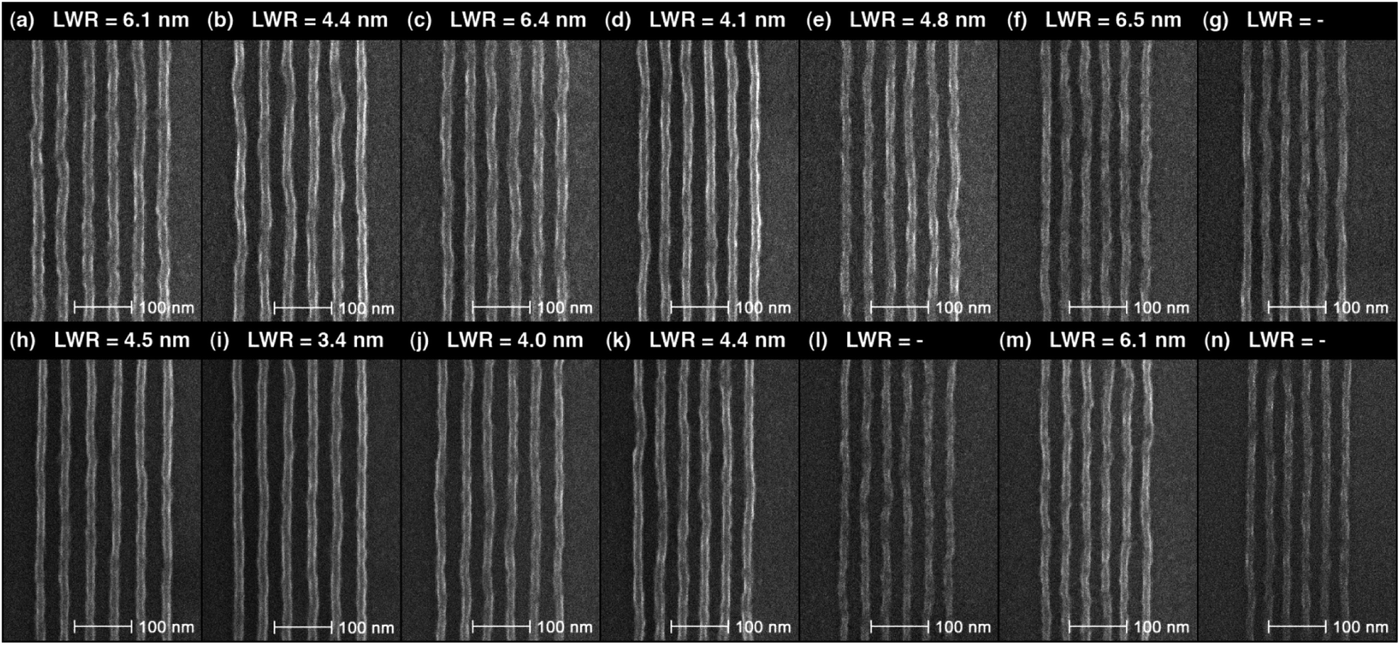
A series of single pixel lines was patterned at various pitches using a beam voltage of 30 keV to evaluate the resolution capability of the resists. Fig. 3 shows isolated features and ∼20 nm lines on a 50 nm pitch in the IM-MFPT12-8 resist with doses between 240 and 350 pC cm−1, using the four developers employed in the previous section. The resist film thickness was approximately 30 nm in this test and the lines were all clearly resolved without pattern collapse. | ||
| Fig. 3 SEM micrographs of patterns in IM-MFPT12-8 developed with (from left to right) MCB–IPA [1:1], cyclohexanone, 2-heptanone, or n-butyl acetate. Isolated features with doses: (a) 350 pC cm−1, (b) 260 pC cm−1, (c) 350 pC cm−1, and (d) 350 pC cm−1. Dense features of ∼20 nm lines on a 50 nm pitch at doses of (e) 240 pC cm−1, (f) 260 pC cm−1, (g) 290 pC cm−1, and (h) 350 pC cm−1. | ||
Table 1 shows the measured feature sizes and LWR (3σ) of the various lines in Fig. 3. Though with ∼1 nm variation in the values of line width and LWR, the overall performances of the four developers were similar. All the four developers showed the capability of resolving sub-15 nm sparse lines as well as 50 nm pitch semi-dense lines with low LWR. All four developers were seen to fully dissolve the unexposed fullerene at concentrations in excess of 100 g l−1, whilst residues were seen when dissolving unexposed epoxy at ∼30 g l−1 for the n-butyl acetate, ∼50 g l−1 for the 2-heptanone, ∼80 g l−1 for the MCB–IPA [1:1], and not seen for the cyclohexanone. Thus, whilst the interaction of the developers with multicomponent films is likely to be complex, it can be qualitatively postulated that cyclohexanone is more aggressive than MCB–IPA [1:1] and 2-heptanone, whilst n-butyl acetate is the poorest solvent for the epoxy component. The correlation of aggressive solvent with high resolution but reduced pattern quality has been noted elsewhere.45 Developer temperature and ultrasonic-assisted development have been shown to affect the quality of patterns in polymeric resists. Fig. S1 and S2 in the ESI† show that these techniques do not significantly affect the processing of this system, although elevated temperature development led to increased substrate residues.
| Developer | Isolated line linewidth [nm] | Isolated line LWR 3σ [nm] | Dense lines linewidth [nm] | Dense lines LWR 3σ [nm] |
|---|---|---|---|---|
| MCB–IPA [1:1] |
13.9 | 2.6 | 18.3 ± 0.1 | 3.8 ± 0.1 |
| Cyclo-hexanone | 13.6 | 3.5 | 17.0 ± 0.1 | 4.1 ± 0.2 |
| 2-Heptanone | 14.6 | 2.6 | 17.1 ± 0.1 | 4.0 ± 0.1 |
| n-Butyl acetate | 14.4 | 3.8 | 18.3 ± 0.1 | 5.1 ± 0.4 |
Post-development bake (hardbake) is sometimes applied to resists to improve resolution or etch selectivity. Whilst the etch performance of this material is excellent even without a post-development bake, it is seen (S3†) that a small reduction in line width and line edge roughness occurs for a 90 °C 5 min hardbake, possibly due to evaporation of residual developer. Such processing also improves the post development stability of line widths as shown in S4.† Post development swelling is most likely due to absorption of humidity and the heat treatment may lead to densification or additional crosslinking which reduces the uptake of water.
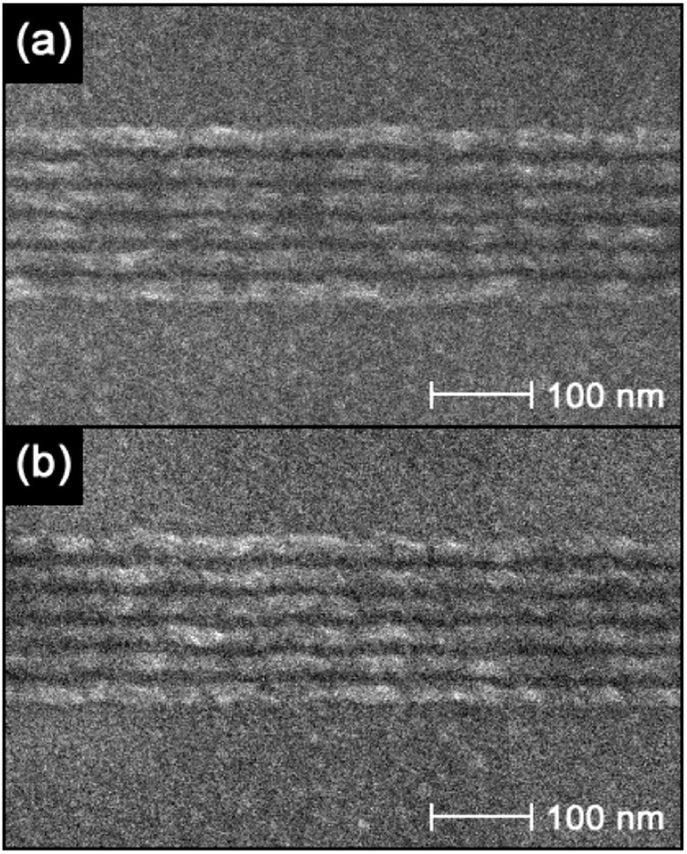
Dense single pixel lines at pitches from 48 nm down to 36 nm were patterned in IM-MFPT12-8 without PEB and with a 90 °C, 1 min PEB, and with MCB–IPA development in both cases, as shown in Fig. 4. Lines from 48 nm pitch down to 36 nm pitch were clearly resolved both with and without PEB, indicating a low activation energy for this resist. A 20–25 nm thickness film of IM-MFPT12-8 was used in this test to avoid pattern collapse in the dense patterns. However, such a thin film also increased LWR compared with the patterns on a 30 nm film. The exposure dose required for the samples without PEB (240–350 pC cm−1) was slightly higher than those with 90 °C, 1 min PEB (230–300 pC cm−1). The measured LWR (3σ) of the lines with various pitch sizes was also shown in Fig. 4. It was found that above 42 nm pitch, the PEB treated lines had smaller LWR than those without PEB. However, below 42 nm pitch, the LWR values reached a similar level for both two groups. This result indicates that, though the crosslinking happens before PEB, the baking process still helps smoothen the pattern edges as in the cases of some other polymer resists46 for instance by driving the crosslinking reaction to completion. On the other hand, the PEB process also increases acid diffusion which is particularly disadvantageous at small pitch sizes.47 In addition, exposure latitude also tends to be narrower with feature size shrink, making the line width and edge roughness more difficult to control,48 Therefore, the PEB process applied in this test did not effectively improve the LWR for dense lines below 42 nm pitch.
 | ||
| Fig. 4 SEM micrographs of single pixel lines written at decreasing pitches in IM-MFPT12-8, and (top; a–g) without PEB and, (bottom; h–n) with 90 °C, 1 min PEB and, in both cases, developed in MCB–IPA [1:1]. The pitches are (from left to right) 48 nm, 46 nm, 44 nm, 42 nm, 40 nm, 38 nm, and 36 nm. | ||
In contrast, the high-sensitivity deproctected derivative, IM-MFP12-3, showed no capability for sub-25 nm half-pitch patterning. However, the best resolution was achieved by mixing IM-MFPT12-2 with IM-MFP12-3. While keeping the 1:2:1 composition ratio of fullerene derivative, crosslinker and PAG constant, the fullerene derivative was changed to a mixture of 75% of IM-MFPT12-2 and 25% of IM-MFP12-3. As shown in Fig. 5, 16 nm and 15 nm half-pitch dense lines were obtained with line doses of 527 pC cm−1 and 478 pC cm−1, respectively. Though the roughness was relatively high due to the strong proximity effect for such dense features at 30 keV patterning, there was no obvious bridging or collapse.
 | ||
| Fig. 5 SEM Micrographs of dense single pixel features on (a) 32 nm, and (b) 30 nm pitches in a mixed IM-MFPT12-2–IM-MFP12-3 [3:1] resist, developed in MCB–IPA [1:1]. | ||
Conclusions
A phenol-based fullerene negative tone resist has been presented for next generation e-beam lithography. Chemical amplification was realized by mixing the fullerene derivative with an epoxy crosslinker and a photo-acid generator. The sensitivity of the IM-MFPT12-8 resist under 20 keV electron beam irradiation was measured to be 43 μC cm−2 with monochlorobenzene and isopropyl alcohol developer. Similar sensitivity were achieve with some more industrially preferred developers, specifically cyclohexanone (46 μC cm−2), 2-heptanone (42 μC cm−2) and n-butyl acetate (42 μC cm−2). Isolated features down to 13.6 nm line width and dense lines:spaces down to 18 nm half-pitch were achieved in the IM-MFPT12-8 resist under 30 keV electron beam exposure. The lithographic performance of the MFPT12-8 resist therefore exceeds the ITRS target of 20 nm DRAM half-pitch for 2016 in both sensitivity and resolution. The effect of post-exposure bake on the line width roughness was investigated, showing that the post-exposure bake reduces line width roughness at larger pitches. However, for pitches below 42 nm, similar line width roughness was observed with and without post-exposure bake. Finally, dense lines down to 15 nm half-pitch were achieved from a mixed IM-MFPT12-2–IM-MFP12-3 [3:1] resist at a slightly higher dose of 478 pC cm−1, which suggests that a partially deprotected tBOC material is worth further study. Plasma etching shows that this resist has high durability. In summary, this new phenol-based fullerene derivative has shown promising results including high sensitivity and resolution, low line width roughness, high etch resistance and industrial compatibility in processing. Further study is required to investigate the crosslinking mechanism of this novel fullerene derivative with tBOC protecting end groups.
Acknowledgements
The authors would like to thank the Engineering and Physical Sciences Research Council (EPSRC) for support of this project. The authors thank Irresistible Materials Ltd. for support and provision of resist materials. The Disco DAD 321 wafer dicer used in this research was obtained through the Birmingham Science City provided: Creating and Characterizing Next Generation Advanced Materials, with support from Advantage West Midlands (AWM) and part funded by the European Regional Development Fund (ERDF). D.X.Y. thanks The University of Birmingham and China Scholarship Council (CSC) for support.Notes and references
- G. E. Moore, Electronics, 1965, 38, 114 Search PubMed.
- G. E. Moore, ISSCC Digest of Technical Papers, 2003, vol. 46, p. 20 Search PubMed.
- International Technology Roadmap for Semiconductors, http://www.itrs.net, accessed online 2013.
- O. Nozawa, H. Shishido, M. Hashimoto, Y. Ohkubo and H. Mitsui, Proc. SPIE, 2010, 7823, 78230K CrossRef.
- T. Kimura, J. Photopolym. Sci. Technol., 2012, 25, 115 CrossRef CAS.
- C. Lapeyre, S. Barnola, I. Servin, S. Gaugiran, V. Salvetat, N. Magome, A. J. Hazelton and M. McCallum, Proc. SPIE, 2009, 7274, 72740W CrossRef.
- M. A. McCord and M. J. Rooks, in Handbook of microlithography, micromachining, and microfabrication, ed. P. Rai-Choudhury, IEE, London, UK, 1997, vol. 1, ch. 2, p. 143 Search PubMed.
- M. A. McCord, P. Petric, U. Ummethala, A. Carroll, S. Kojima, L. Grella, S. Shriyan, C. T. Rettner and C. F. Bevis, Proc. SPIE, 2012, 8323, 832311 CrossRef.
- C. Klein, H. Loeschner and E. Platzgummer, J. Micro/Nanolithogr., MEMS, MOEMS, 2012, 11, 031402 CrossRef.
- J. Belledent, M. Smayling, J. Pradelles, P. Pimenta-Barros, S. Barnola, L. Mage, B. Icard, C. Lapeyre, S. Soulan and L. Pain, Proc. SPIE, 2012, 8323, 83230F CrossRef.
- E. Slot, M. J. Wieland, G. De Boer, P. Kruit, G. F. Ten Berge, A. M. C. Houkes, R. Jager, T. Van De Peut, J. J. M. Peijster, S. W. H. K. Steenbrink, T. F. Teepen, A. H. V. Van Veen and B. J. Kampherbeek, Proc. SPIE, 2008, 6921, 69211P CrossRef.
- W. W. Hu, K. Sarveswaran, M. Lieberman and G. H. Bernstein, J. Vac. Sci. Technol., B: Microelectron. Nanometer Struct.–Process., Meas., Phenom., 2004, 22, 1711 CrossRef CAS.
- S. Yasin, D. G. Hasko and H. Ahmed, Microelectron. Eng., 2002, 61, 745 CrossRef.
- B. Shokouhi, J. Zhang and B. Cui, Micro Nano Lett., 2011, 6, 12 Search PubMed.
- J. Reinspach, M. Lindblom, O. von Hofsten, M. Bertilson, H. M. Hertz and A. Holmberg, J. Vac. Sci. Technol., B: Microelectron. Nanometer Struct.–Process., Meas., Phenom., 2009, 27, 2593 CrossRef CAS.
- J. K. Yang, B. Cord, H. Duan, K. K. Berggren, J. Klingfus, S. W. Nam, K. B. Kim and M. J. Rooks, J. Vac. Sci. Technol., B: Microelectron. Nanometer Struct.–Process., Meas., Phenom., 2009, 27, 6 CrossRef.
- J. Kim, W. Chao, B. Griedel, X. Liang, M. Lewis, D. Hilken and D. L. Olynick, J. Vac. Sci. Technol., B: Microelectron. Nanometer Struct.–Process., Meas., Phenom., 2009, 27, 2628 CrossRef CAS.
- J. Fujita, Y. Ohnishi, Y. Ochiai and S. Matsui, Appl. Phys. Lett., 1996, 68, 1297 CrossRef CAS.
- H. Duan, D. Winston, J. K. W. Yang, B. M. Cord, V. R. Manfrinato and K. K. Berggren, J. Vac. Sci. Technol., B: Microelectron. Nanometer Struct.–Process., Meas., Phenom., 2010, 28, C6C58 CAS.
- S. Ma, C. Con, M. Yavuz and B. Cui, Nanoscale Res. Lett., 2011, 6, 446 CrossRef PubMed.
- R. A. Lawson, L. M. Tolbert, T. R. Younkin and C. L. Henderson, Proc SPIE, 2009, 7273, 72733E CrossRef.
- E. Herth, E. Algre, P. Tilmant, M. Francois, C. Boyaval and B. Legrand, IEEE Trans. Nanotechnol., 2012, 11, 4 CrossRef.
- H. Ito, C. G. Willson and J. M. J. Frechet, Digest of Technical Papers, Symposium on VLSI Technology, 1982, pp. 86–87 Search PubMed.
- H. Ito and C. G. Willson, Polym. Eng. Sci., 1983, 23, 1012 CAS.
- T. H. Fedynyshyn, R. B. Goodman and J. Roberts, Proc. SPIE, 2008, 6923, 692319 CrossRef.
- J. T. Woodward, T. H. Fedynyshyn, D. K. Astolfi, S. C. Cann, J. M. Roberts and M. J. Leeson, Proc. SPIE, 2007, 6519, 651915 CrossRef.
- T. Kadota, H. Kageyama, F. Wakaya, K. Gamo and Y. Shirota, Chem. Lett., 2004, 33, 706 CrossRef CAS.
- H. M. Zaid, A. P. G. Robinson, R. E. Palmer, M. Manickam and J. A. Preece, Adv. Funct. Mater., 2007, 17, 2522 CrossRef CAS.
- D. Drygiannakis, G. P. Patsis, N. Tsikrikas, G. Kokkoris, A. Boudouvis, I. Raptis, E. Gogolides and P. Argitis, Microelectron. Eng., 2008, 85, 949 CrossRef CAS.
- J. Manyam, M. Manickam, J. A. Preece, R. E. Palmer and A. P. G. Robinson, Proc. SPIE, 2009, 7273, 72733D CrossRef.
- F. P. Gibbons, H. M. Zaid, M. Manickam, J. A. Preece, R. E. Palmer and A. P. G. Robinson, Small, 2007, 3, 2076 CrossRef CAS PubMed.
- J. Manyam, M. Manickam, J. A. Preece, R. E. Palmer and A. P. G. Robinson, Proc. SPIE, 2011, 7972, 79722N CrossRef.
- T. Tada, T. Kanayama, A. P. G. Robinson, R. E. Palmer, M. T. A. Allen, J. A. Preece and K. D. M. Harris, Microelectron. Eng., 2000, 53, 425 CrossRef CAS.
- H. Sailer, A. Ruderisch, D. P. Kern and V. Schurig, Microelectron. Eng., 2004, 73–74, 228 CrossRef CAS.
- R. A. Lawson, C.-T. Lee, L. M. Tolbert, T. R. Younkin and C. L. Henderson, Microelectron. Eng., 2009, 86, 734 CrossRef CAS.
- H. Oizumi, K. Tanaka, K. Kawakami and T. Itani, Jpn. J. Appl. Phys., 2010, 49, 06GF04 CrossRef.
- J. Manyam, A. Frommhold, D. X. Yang, A. McClelland, M. Manickam, J. A. Preece, R. E. Palmer and A. P. G. Robinson, Proc. SPIE, 2012, 8325, 83251U CrossRef.
- A. Frommhold, D. X. Yang, A. McClelland, X. Xiang, Y. Ekinci, R. E. Palmer and A. P. G. Robinson, J. Micro/Nanolithogr., MEMS, MOEMS, 2013, 12(3), 033010 CrossRef.
- C. Bingel, Chem. Ber., 1993, 126, 1957 CrossRef CAS.
- X. Camps and A. Hirsch, J. Chem. Soc., Perkin Trans. 1, 1997, 1595 RSC.
- F. P. Gibbons, A. P. G. Robinson, R. E. Palmer, S. Diegoli, M. Manickam and J. A. Preece, Adv. Funct. Mater., 2008, 18, 1977 CrossRef CAS.
- T. Karatsu, Y. Yoshimura, S. Miura, S. Yagai, A. Kitamura, J. Ozaki and H. Okamoto, J. Photopolym. Sci. Technol., 2011, 24, 5 CrossRef.
- I. Takemoto, Y. Fuji, I. Yoshida, K. Hashimoto, T. Miyagawa, S. Yamaguchi, K. Takahashi, S. Konishi and Y. Lee, J. Photopolym. Sci. Technol., 2005, 18, 3 CrossRef.
- H. Yamamoto, T. Kozawa, S. Tagaway, H. B. Cao, H. Deng and M. J. Leeson, Jpn. J. Appl. Phys, 2007, 46, L142 CrossRef CAS.
- D. L. Olynick, P. D. Ashby, M. D. Lewis, T. Jen, H. Lu, J. A. Liddle and W. Chao, J. Polym. Sci., Part B: Polym. Phys., 2009, 47, 2091 CrossRef CAS.
- D. S. H. Hsu, W. H. Hsieh, C. Y. Huang, W. B. Wu and C. L. Shih, Proc. SPIE, 2012, 8325, 83251M CrossRef.
- K. Cho, S. Tarutani, N. Inoue, H. Tsubaki and M. Neisser, Proc. SPIE, 2013, 8682, 868217 CrossRef.
- T. Kozawa, H. Oizumi, T. Itani and S. Tagawa, Jpn. J. Appl. Phys., 2011, 50, 126501 CrossRef.
Footnote |
| † Electronic supplementary information (ESI) available: Additional development and post-development processes. See DOI: 10.1039/c3tc31896f |
| This journal is © The Royal Society of Chemistry 2014 |