 Open Access Article
 This Open Access Article is licensed under a
 Creative Commons Attribution 3.0 Unported Licence
Structure–function relations in diF-TES-ADT blend organic field effect transistors studied by scanning probe microscopy†
Aaron B.
Naden
*,
Joachim
Loos
and
Donald A.
MacLaren
*
SUPA, School of Physics and Astronomy, University of Glasgow, Glasgow, G12 8QQ, UK. E-mail: a.naden.1@research.gla.ac.uk; dmaclaren@physics.org
First published on 13th November 2013
Abstract
We develop structure–property relations for organic field effect transistors using a polymer/small-molecule blend active layer. An array of bottom gate, bottom contact devices using a polymeric dielectric and a semiconductor layer of 2,8-difluoro-5,11-bis(triethylsilylethynyl)anthradithiophene (diF-TES-ADT) is described and shown to have good device-to-device uniformity. We describe the nucleation and growth processes that lead to the formation of four structurally distinct regimes of the diF-TES-ADT semiconductor film, including evidence of layer-by-layer growth when spin-coated onto silver electrodes and an organic dielectric as part of a polymer blend. Devices exhibiting a maximum saturation mobility of 1.5 cm2 V−1 s−1 and maximum current modulation ratio (Ion/Ioff) of 1.20 × 10⁵ are visualised by atomic force microscopy and appear to have excellent domain connectivity and aligned crystallography across the channel. In contrast, poorly performing devices tend to show a phase change in semiconductor crystallinity in the channel centre. These observations are enhanced by direct visualisation of the potential drop across the channel using Kelvin probe microscopy, which confirms the importance of large, well-aligned and well-connected semiconductor domains across the transistor channel.
Introduction
An essential component for the realisation of cheap, fully-flexible ‘plastic’ electronics is an organic field-effect transistor (OFET) using an organic semiconductor (OSC) thin film to form the basis of switching, logic, storage or sensor devices.1–3 Extensive research into the synthesis and processing of polycrystalline OSCs has enabled electron hole mobilities in excess of 1 cm2 V−1 s−1 to be demonstrated,4 rivalling the performance of hydrogenated amorphous silicon thin film devices.5 However, substantial challenges still remain in optimising physicochemical aspects including rheology and crystallisation kinetics, particularly when using solution-phase processing protocols, which offer the most cost-effective routes to mass production.6 Early studies focused on conductive polymers that are relatively easy to process and are robust to variations but gave typically poor electronic performance, including hole mobilities of around 0.1 cm2 V−1 s−1.7 Small molecules, on the other hand, can support remarkably high hole mobilities, but are notoriously difficult to process on large scales due to their tendency to crystallise rapidly.8 Substantial interest was therefore generated by recent progress in combining, as a blend, the large-area processability of polymers with the high mobility performance of small molecules. In this context, blends containing derivatives of pentacene9 or anthradithiophenes10 have shown great promise, with charge conduction enhanced by good π-orbital overlap between molecules.11 Of the small molecules currently known, the fluorinated anthradithiophene known as diF-TES-ADT [2,8-difluoro-5,11-bis(triethylsilylethynyl)anthradithiophene, Fig. 1a] is amongst the most promising p-type candidate OSCs. Fluorine–fluorine and fluorine–sulphur interactions between adjacent molecules are believed to improve crystallinity and stability,4 thereby improving π-orbital alignment and resulting in the single crystal form having a measured hole mobility of up to 6 cm2 V−1 s−1.12 Lower mobilities – typically between 0.1 and 1.0 cm2 V−1 s−1 – have been reported when diF-TES-ADT is spin-cast from solution, a processing step that can be applied on large scales.4 A number of studies have also explored the use of diF-TES-ADT in a blend, usually with conductive polytriarylamines (PTAAs), and have shown retention of diF-TES-ADT's intrinsic high performance, with mobilities above 2 cm2 V−1 s−1.13 Although a variety of different device architectures exist,10,14 most research using polymer/small molecule blends has employed so-called top gate devices, where the gate material is deposited last. The reasoning is twofold: firstly, the gate dielectric of a top-gate device is in closer proximity to the diF-TES-ADT since the blend is known to undergo vertical phase segregation;13 secondly, if the alternative bottom gate architecture is used, then there are known difficulties in uniformly spin-casting the diF-TES-ADT/PTAA blend onto the polymeric dielectric that is required for fully-flexible devices.10 Nevertheless, a strong advantage of bottom gate, bottom contact (BGBC) devices is that the most process-sensitive component – the semiconductor layer – is deposited in the final step, avoiding exposure to any potentially detrimental processing conditions that are required for other layers in the stack, such as metal electrodes. Here, we present a structural and functional study of such bottom-gate, bottom contact (Fig. 1b) OFETs using a diF-TES-ADT-containing blend that exhibits hole mobilities in excess of 1 cm2 V−1 s−1 with good device-to-device uniformity. We use optical and scanning probe microscopies to study the segregation, crystallisation and resulting function of diF-TES-ADT. Understanding the effect of processing on semiconductor crystallisation is essential since a high hole mobility across a device depends on both the nature of molecular packing at nanometric length-scales and the morphology and arrangement of domains that can span tens of microns.15 Furthermore, crystallisation – and hence optimised OFET function – is intimately related to subtle processing details, so that device-to-device variability remains problematic in OFET design and substantial characterisation is required for each new small molecule, process reagent or even blend ratio that is proposed. Our study is also a rare example of structural characterisation of diF-TES-ADT crystallisation out of a blend and atop a polymeric dielectric layer, which contrasts with the more common usage of hard inorganic dielectrics such as silica4 that show reduced mobility performance because of energetic disorder at the dielectric–semiconductor interface.16 Although the substrate influences the crystallisation of a thin film through surface energy differences, relative hydrophobicity and issues of dewetting,17 we show that good crystallographic control and grain growth can be maintained with high electronic mobility and reasonable variability. This is a critical step in the development of fully flexible, high mobility OFETs.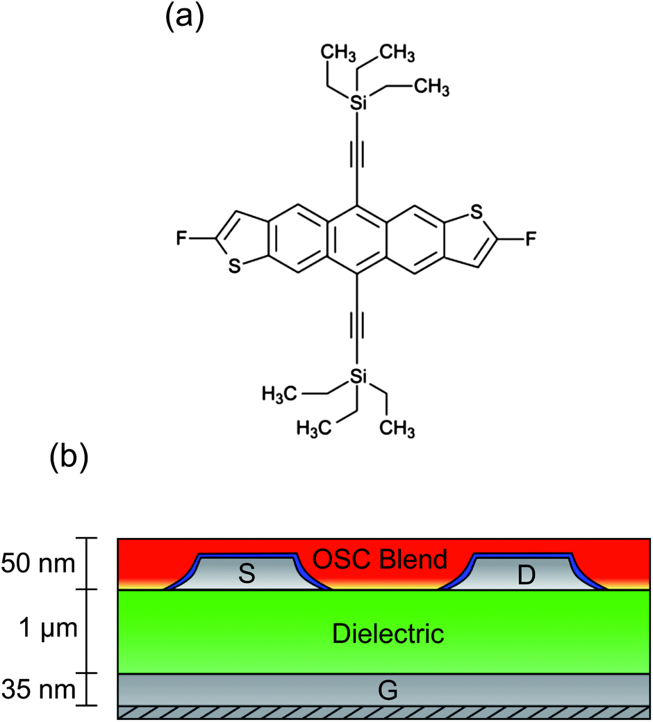 | ||
| Fig. 1 (a) Chemical structure of 2,8-difluoro-5,11-bis(triethylsilylethynyl)anthradithiophene (diF-TES-ADT). (b) Schematic cross section of the bottom gate, bottom contact (BGBC) device architecture. | ||
Experimental
Sample preparation
Bottom gate, bottom contact (BGBC) devices were fabricated on glass substrates. A silver bottom gate electrode was thermally evaporated through a shadow mask to a final thickness of approximately 35 nm. A 1 μm thick proprietary cross-linkable dielectric was spin-cast and cross-linked. Silver source and drain electrodes were evaporated under vacuum in an identical manner to above and were treated by immersion in a solution of 2,3,4,5,6-pentafluorobenzenethiol (PFBT) in isopropyl alcohol. The active layer was spin cast from a blend of 2,8-difluoro-5,11-bis(triethylsilylethynyl)anthradithiophene (diF-TES-ADT) and an insulating and amorphous polystyrene-type polymer binder, then annealed under ambient conditions, resulting in a film approximately 50 nm thick. Once dried, the blend has a relatively high diF-TES-ADT![[thin space (1/6-em)]](https://www.rsc.org/images/entities/char_2009.gif) :polymer mass ratio, which is substantially above the minimum threshold required for vertical phase segregation and lateral percolation, but which is expected to perform better than neat diF-TES-ADT.18 Vertical phase segregation was confirmed to have occurred using energy filtered transmission electron microscopy (EFTEM) and implies that the exact chemical nature of the dielectric is of limited importance to subsequent OSC crystallisation, since the binder segregates at the dielectric interface. As described elsewhere19 mesitylene was chosen as the solvent because it better solvates anthradithiophenes such as diF-TES-ADT and is slower to evaporate, giving more time for crystallisation of the small molecule OSC. Mesitylene is also preferable to the use of chlorinated solvents, whose usage still dominates the field but is environmentally undesirable, particular for large-scale manufacturing. Reference devices were fabricated as above but using 6,13-bis(triisopropylsilylethynyl)-pentacene (TIPS-PEN) as the semiconductor.
:polymer mass ratio, which is substantially above the minimum threshold required for vertical phase segregation and lateral percolation, but which is expected to perform better than neat diF-TES-ADT.18 Vertical phase segregation was confirmed to have occurred using energy filtered transmission electron microscopy (EFTEM) and implies that the exact chemical nature of the dielectric is of limited importance to subsequent OSC crystallisation, since the binder segregates at the dielectric interface. As described elsewhere19 mesitylene was chosen as the solvent because it better solvates anthradithiophenes such as diF-TES-ADT and is slower to evaporate, giving more time for crystallisation of the small molecule OSC. Mesitylene is also preferable to the use of chlorinated solvents, whose usage still dominates the field but is environmentally undesirable, particular for large-scale manufacturing. Reference devices were fabricated as above but using 6,13-bis(triisopropylsilylethynyl)-pentacene (TIPS-PEN) as the semiconductor.
Microscopy
A Meiji FU1000 was used for polarised optical microscopy under cross polarised conditions and an NT-MDT Solver Px Next was used for atomic force microscopy (AFM), using NSG11 and NSG03 tips (also purchased from NT-MDT) for tapping mode AFM. Pt-coated DPE18 tips purchased from MikroMasch were used for scanning Kelvin probe microscopy (KPM). Focused ion beam (FIB) preparation of cross-sectional transmission electron microscopy (TEM) specimens was performed using standard techniques on an FEI Nova Dual Beam instrument, with ion beam accelerating voltages of 16, 8 and finally 5 kV. In order to prevent charging of the sample in the FIB, layers of carbon and aluminium around 30 nm thick were deposited on top of the sample, with the carbon layer ensuring no implantation of aluminium into the active layer of the device. Cross-sectional lamellae were thinned to ca. 60 nm thick for TEM analysis. TEM was performed on an FEI Tecnai T20 instrument operating at 200 kV and equipped with a LaB6 electron source and Gatan Imaging Filter. The latter was used for energy filtered TEM, using a standard three-window technique to extrapolate a power-law background trend under the electron energy loss feature of interest.Electrical characterisation
An Agilent 4155C Semiconductor Parameter Analyser was used to measure transfer characteristics. Saturation and linear mobilities were derived as described elsewhere,20 with the drain current (ID) measured at a drain voltage (VD) of −60 V and −5 V, respectively.Results and discussion
Electrical characteristics
We first consider OFET electrical characteristics and their statistics, based on our characterisation of 86 devices with channel length of 50 μm and width of 1 mm, using the architecture sketched in Fig. 1b. Devices of 50 μm channel length gave the optimum performance and will be described in detail here. Devices with shorter channel lengths were also fabricated but exhibited substantially reduced hole mobilities: the maximum measured μsat was 0.83 and 0.48 cm2 V−1 s−1 for 20 μm and 10 μm channel length devices, respectively. This result differs from the more usual reduction in mobility with channel length due to contact resistance arising from injection barriers21 but which correlates with structural features observed using scanning probe microscopy, as explored in the ESI.† To illustrate the variability of device performance, Fig. 2a shows the distribution of hole mobilities measured in the saturation regime, μsat, for 50 μm devices. The majority of OFETs exhibit saturation mobilities in excess of 1 cm2 V−1 s−1, with a maximum of 1.5 cm2 V−1 s−1 and standard deviation of 0.2 cm2 V−1 s−1. The maximum measured linear mobility was 1.2 cm2 V−1 s−1 and all but one device showed good transistor characteristics. There was no strong correlation between a device's location on the substrate and its electrical performance. To our knowledge, this performance exceeds that previously published for BGBC devices incorporating diF-TES-ADT as a blend. Fig. 2b provides further characterisation of a typical device. It depicts the drain current, ID (left-hand ordinate), measured as a function of gate voltage, VG, when the drain voltage, VD, was held at −5 V (linear regime) and −60 V (saturation regime) with respect to the source. The linear regime occurs when VD < VG and the drain current increases linearly with gate voltage, whereas the saturation regime corresponds to VD > VG, at which point the drain current saturates.20 Also plotted (right hand ordinate) are the derived saturation (μsat) and linear (μlin) mobility characteristics of the same device, which are representative of the average performance. The device shows a threshold voltage, Vth, of ∼ −14 V and the gate voltage required to turn the device ‘off’ is ∼ +1 V. There is minimal hysteresis and no observed degradation in performance over several cycles. This performance is in contrast to that of Fig. 2c, measured from the statistical ‘outlier’ device that had substantially impaired electrical performance. The data of Fig. 2c show a much poorer defined switching threshold, a reduction in drain current, pronounced hysteresis in I–V response, and substantially reduced on–off ratios and mobilities. In this case the peak saturation mobility was 0.08 cm2 V−1 s−1. The reduced drain currents (implying an undesirable increased resistance) and slower response to an applied bias of this device make it unsuitable for use. Both aspects can be explained in terms of structural characteristics of the OSC film, as will be explored below. Hysteresis in particular has been ascribed to charge trapping and then charge liberation at domain boundaries and defects as VG is cycled.22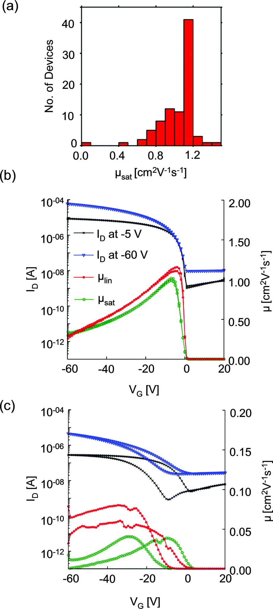 | ||
| Fig. 2 (a) Histogram showing the statistical distribution of measured saturation mobilities measured from 86 devices. (b) and (c) I–V graphs showing the modulus of the drain current (left-hand ordinate) and mobility (right-hand ordinate) of a high and a low performance device, respectively. | ||
Morphological characterisation
A low magnification polarised optical microscopy (POM) image of a typical OFET device is presented in Fig. 3a. Contrast in the image is dominated by reflection from the bottom electrode and birefringence of the semiconductor (noting that the dielectric layer is amorphous and flat and therefore can be disregarded in this context). The image is therefore immediately interpretable as indicating a number of small crystalline grains decorating the silver electrodes in addition to larger, planar crystalline semiconductor domains that lie roughly normal to the electrode boundaries, extend up to ∼40 μm into the channel and meet at well-defined domain boundaries along the channel centre. Crystals are typically much broader than those observed in comparable 6,13-bis(triisopropylsilylethynyl)pentacene [TIPS-PEN] devices6 (see ESI, Fig. S2†) and there is greater directionality to the grains spreading into the channel and interleaving than in recent studies showing crystallisation on SiOx,13,23 however their structures are quite similar to those seen with neat diF-TES-ADT.4 Grain nucleation within the channel seems to be almost completely suppressed, which is desirable as homonucleation within the channel has been shown to be problematic.24,25 Colour and contrast variations between domains hint at slight domain-by-domain differences in molecular orientation, providing a rapid, qualitative assessment of the connectivity of domains within the channel and of the impact of domain boundaries on the hole mobilities measured above. Similar colours between neighbouring crystalline domains suggest better molecular alignment across the boundary and better electrical characteristics if considering charge transport via the hopping mechanism.26,27Fig. 3a already demonstrates the high quality nature of these OFET devices.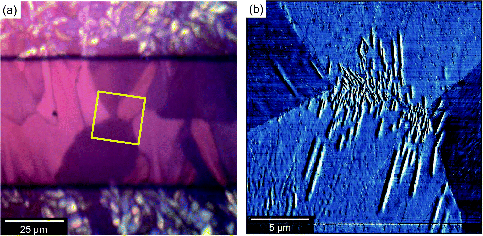 | ||
| Fig. 3 (a) Polarised optical micrograph showing the channel of an L = 50 μm device. Small semiconductor grains can be seen on top of the electrodes and large domains can be seen to extend into the channel. (b) An AFM phase image corresponding to the region indicated by the yellow box in (a). Some domain-by-domain contrast can be seen in agreement with the colour contrast in (a). | ||
Atomic force microscopy (AFM) provides an enhanced overview of the morphology of the OSC surface, which is uppermost in BGBC devices and so is immediately accessible to scanning probe microscopies. An AFM image of a typical device is presented in the middle portion of Fig. 4. The upper portion of Fig. 4 is a POM image of the same area. The area spans outwards from the source electrode into the ‘bulk’ (i.e. on the other side of the electrode to the channel), so as to show the full extent of crystallisation without interaction with domains extending in the opposite direction, from an opposing electrode. The figure shows a large domain extending from a nucleation point on top of the electrode (left), out and across the dielectric. There are distinctive ribbed thickness variations within the AFM image but the domain boundaries that are clear in the POM image are harder to discern, indicating an almost continuous film. On the basis of this and higher magnification images, we identify four distinct structural regimes consistent with a crystal nucleation and growth mechanism and illustrated in the cross-sectional cartoon of Fig. 4c. The long axis of this figure can be considered as a ‘timeline’ of sorts, due to the sequential formation of the different crystal regimes, which we will now address in turn.
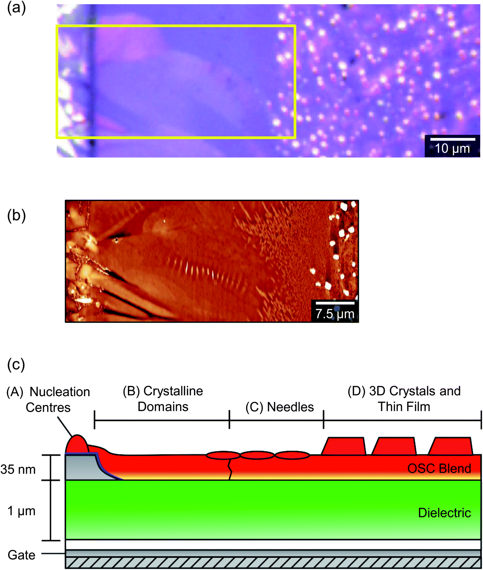 | ||
| Fig. 4 (a) Polarised optical micrograph of the edge of a typical device, in an area, from left to right, moving out from the source/drain electrode. (b) AFM image of the same region. It is to be noted that not all the 3D crystals that are visible in the AFM image appear in the optical micrograph due to the lower magnification and specific optical alignment of the latter. (c) Schematic cross-sectional cartoon of a similar area, derived from the AFM analysis and showing four structurally distinct crystalline regimes. | ||
The initial stage of film formation (regime A of Fig. 4) is the nucleation of diF-TES-ADT grains on top of the PFBT-treated electrodes. Fig. 5 shows a typical region of the electrode, with distinct, localised protrusions (which we identify as nucleation centres) around 50 ± 10 nm above the OSC film, from which grains grow laterally, along the device surface. Unlike truly spherulitic growth,28 grains do not appear to grow isotropically from a nucleation centre, and instead exhibit distinctive ‘petal’ shapes (Fig. 5) arising from the grains' underlying crystallography and which are largely in agreement with the literature.4,27 The number density of nucleation centres on top of the electrodes is of order 0.03 μm−2, substantially below the density of either the underlying Ag crystallites, which is of order 70 μm−2 (see ESI, Fig. S3†), or of agglomerated PFBT islands29 that are deposited on the electrode surfaces. Both of the latter surfaces are rough but otherwise isotropic and we find no evidence of specific structural features that could promote crystal nucleation, which more likely is best described on a statistical basis. Thus, the relatively low number of nucleation sites and large size of grains indicates that nucleation is rate-limiting. Once nucleated, grains grow rapidly until solvated OSC molecules are exhausted. Although some crystallisation is seen to occur in the channel (similar to regime D of Fig. 4), those crystals are small and crystallographically distinct, as will be described below. The absence of petal nuclei within the channel indicates that the kinetics for petal nucleation in the absence of electrodes are substantially slower. Since nucleation of large, petal-like crystals is exclusive to the tops of electrodes we conclude that they are promoted by the PFBT-treated Ag, showing similarity to PFBT-treated Au electrodes in the literature4,15 but at less cost. Although we can find no precedent for silver electrodes in this context, the interactions of thiols with silver are expected to be similar to those with gold30 – as evidenced by our results. Structurally, Au and Ag evaporated electrodes exhibit comparably rough, polycrystalline surfaces which promote OSC crystallisation. This can be shown by example: nucleation centres are not as numerous in devices where Au electrodes have been evaporated onto SiOx (ref. 4 and 31) or glass,10 where the Au forms much smoother films and the number of potential roughness-induced nucleation sites is reduced. Chemically, the electrode to PFBT thiol linkage is also known to be similar for both Au and Ag,30 and the immobilised PFBT molecules are expected to tether solvated diF-TES-ADT through F–S interactions and F–F interactions15,32,33 in a similar way to those known to operate with the unfluorinated analogue, TES-ADT.34 Without PFBT, nucleation is slowed and we find the density of nucleation centres to be greatly reduced and the continuity of domains within the channel to be impaired, resulting in lower performance.15 In addition, PFBT is also known to improve charge injection from the electrode into the OSC by reducing the Schottky barrier created by the misalignment of the electrode's Fermi level and the highest molecular orbital of the OSC.35 As illustration, devices that we prepared without PFBT had less obvious crystallisation (as evidenced by AFM, see ESI, Fig. S4†) and had a maximum μsat of 0.55 cm2 V−1 s−1 and a maximum Ion/Ioff of 8.40 × 10⁴. Further characterisation of Ag electrodes is provided in the ESI.†
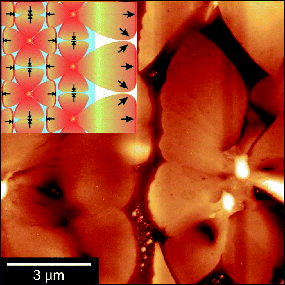 | ||
| Fig. 5 An AFM image collected from atop an electrode, showing petal-like grains fanning out from central nucleation centres. Inset: schematic representation of the grain growth process showing the extension of grains from the electrode (blue) into the bulk (white). | ||
The second regime (B) in Fig. 4 is the growth of long, petal-like OSC crystals into the channel. Once nucleated, grains grow by the oriented accretion of solvated OSC molecules and will be limited by diffusion kinetics. The eventual domain size is dictated primarily by the proximity of adjacent nucleation sites and resultant competition for free diF-TES-ADT molecules, so that only those domains nucleated towards the electrode edges are able to extend into the channel, as depicted schematically in the inset to Fig. 5. These domains may grow tens of microns into the channel, resulting in a domain such as that in the AFM image in the middle panel of Fig. 4. Near the nucleation centre a layered structure is evident, as shown in Fig. 6a and the corresponding AFM phase image in Fig. S5.† The regular succession of steps is consistent with diF-TES-ADT crystallisation, with the uniformity of the AFM phase image suggesting the chemical composition of each exposed plane to be similar. The step heights are measured to be 16.66 ± 0.48 Å (mean ± standard deviation) whilst the ‘pits’ within a given terrace are 16.67 ± 0.31 Å or 31.93 ± 1.24 Å deep; a profile is shown in Fig. 6b. These measurements are in excellent agreement with multiples of the d001 spacing of the triclinic (P![[1 with combining macron]](https://www.rsc.org/images/entities/char_0031_0304.gif) space group) crystal which is 16.3 Å.12 Thus, the AFM data imply that the c axis is aligned along the substrate normal and the a–b plane is parallel to the substrate, the orientation possibly driven by the low interfacial energy of silyl side groups in close proximity to the phase-segregated binder36 which, as will be discussed later, wets the dielectric. This crystallographic orientation is in agreement with a previous study of the crystallisation of neat diF-TES ADT on an insulating substrate12 and our result is interesting because, to the best of our knowledge, such layered structure has only been previously reported for the single crystal form of diF-TES-ADT.12 Importantly, the domains of Fig. 4 are much larger and have less pronounced domain boundaries than those of neat diF-TES-ADT grown on a SiO2 dielectric.4,11 We find that this is critical to performance since pronounced domain boundaries are believed to contain deep charge traps that cause hysteresis37,38 similar to that observed in our ‘bad’ devices produced without PFBT.
space group) crystal which is 16.3 Å.12 Thus, the AFM data imply that the c axis is aligned along the substrate normal and the a–b plane is parallel to the substrate, the orientation possibly driven by the low interfacial energy of silyl side groups in close proximity to the phase-segregated binder36 which, as will be discussed later, wets the dielectric. This crystallographic orientation is in agreement with a previous study of the crystallisation of neat diF-TES ADT on an insulating substrate12 and our result is interesting because, to the best of our knowledge, such layered structure has only been previously reported for the single crystal form of diF-TES-ADT.12 Importantly, the domains of Fig. 4 are much larger and have less pronounced domain boundaries than those of neat diF-TES-ADT grown on a SiO2 dielectric.4,11 We find that this is critical to performance since pronounced domain boundaries are believed to contain deep charge traps that cause hysteresis37,38 similar to that observed in our ‘bad’ devices produced without PFBT.
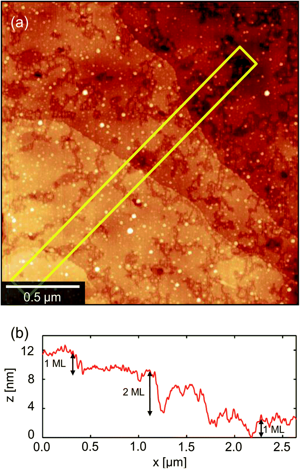 | ||
| Fig. 6 (a) AFM image showing the layered structure near a nucleation centre. Terraces corresponding to monomolecular layers can be seen, with some voids that are also 1 monolayer deep. (b) Height profile across the stepped structure, measured from the box indicated in (a). | ||
Interestingly, phase contrast imaging in AFM affords a degree of sensitivity to molecular orientation within domains. This can be seen in the correlation between Fig. 3b and the region of Fig. 3a indicated by the yellow box, namely that the slightly darker domains observed in Fig. 3a correspond to the lighter regions in Fig. 3b. This remarkable correlation suggests that domains with slightly different molecular orientations (of the order of a few degrees) have slightly different viscoelastic, chemical or mechanical properties, as it is these properties to which AFM phase is known to be sensitive. To our knowledge there have not been any previous reports of such phase-sensitivity in OFETs.
The crystallography described above suggests that the AFM tip interacts with the triethylsilyl side-groups of diF-TES-ADT which terminate the petal surface; interaction with the acene core should be sterically hindered. AFM phase sensitivity to orientational changes of only a few degrees is therefore surprising since the relatively floppy terminating ethyl groups might be expected to have a degree of rotational disorder about the ethynyl bond axis, so that the tip–surface interaction is averaged. (More likely, of course, is that the tip–surface interaction is mediated by a thin adsorbed moisture layer, since all measurements were conducted under ambient conditions.) It can also be seen that there is not a 1:1 correlation between AFM phase contrast and POM colouration. For example, the upper two domains have different colours (i.e. pink and purple) in POM but uniform AFM phase contrast. We are currently exploring these intriguing results in more detail.
Scanning Kelvin probe microscopy (KPM) is a powerful tool for understanding how morphological features can influence the electrical characteristics in operating devices,39 since it can map the electric potential distribution across the OFET accumulation layer.40Fig. 7a shows an enlarged polarised optical micrograph from the centre of the channel of a typical device and Fig. 7b to d show the AFM topography, KPM surface potential and the gradient of the surface potential, respectively, all collected using a drain bias of −1 V and a gate voltage of 0 V. Comparison of the POM and AFM images in Figs. 7a and b allows for easy identification of the boundaries between the domains and it can be seen that the ends of some of the domains are decorated by needle-shaped crystallites, which will be described below as regime C. The contour map of the KPM surface potential in Fig. 7c allows for a correlation between topography and electrical performance and shows a gradual potential drop across the channel that is modulated by the domain boundaries. For example, the boundary to the right of the images has a steeper potential gradient than the boundary on the far left. Fig. 7d shows the gradient of the surface potential calculated from the KPM data, which highlights all of the domain boundaries but is maximised in those regions with the needle-like protrusions in Fig. 7b. A steeper potential gradient indicates poorer electrical connectivity (or greater electrical resistance) and in this instance is greatest across the right-most boundary. Specifically, at VD = −1 V the potential gradient at the domain boundaries ranges from ∼0.04 V μm−1 to ∼0.08 V μm−1 compared to the mean of 0.02 V μm−1 across the 50 μm channel. This suggests that the needle crystallites correlate with a reduction in device performance due to a hindrance in inter-domain transport through the underlying petals. This contrasts to the increased current recently found at grain boundaries in a diF-TES ADT/PTAA system.41
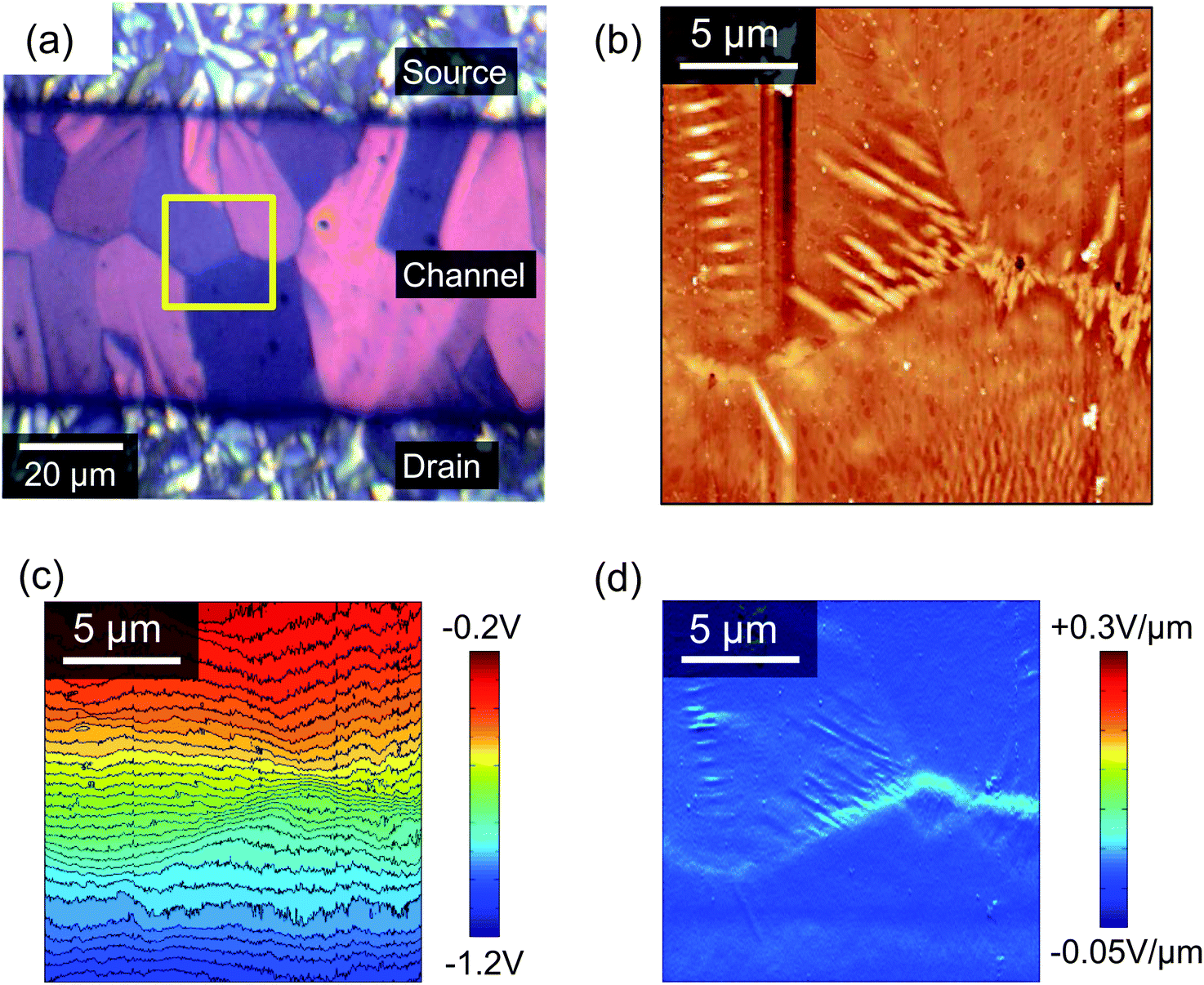 | ||
| Fig. 7 (a) Polarised optical micrograph of the channel of a typical device. (b) AFM topography within the yellow box of (a), showing the domain boundaries and needle-like crystallites as described in previous sections. (c) A contour map of the surface electrical potential measured by KPM and (d) the potential gradient calculated from (c) along the fast-axis scan-direction and perpendicular to the electrodes. The AFM and KPM images were acquired simultaneously and have been treated to remove a small number of scars caused by minor surface contamination and subsequent raster errors. | ||
Returning to a discussion of the crystal growth modes and for comparison with the diF-TES-ADT devices, we additionally fabricated analogous devices using TIPS-PEN as the OSC. The TIPS-PEN molecule has a similar aromatic backbone and bulky alkyl side-groups as diF-TES-ADT but lacks the sulphur and fluorine of diF-TES-ADT and so cannot participate in F–S and F–F intermolecular interactions. Fig. S2 (ESI†) shows long, lath-like TIPS-PEN crystallites extending from the top of the electrodes, consistent with the literature.6,42 However, the crystal habit is notably different to that of diF-TES-ADT. For example, Fig. 5 shows petal-like diF-TES-ADT crystallites fanning out from an easily discernible nucleation centre whilst TIPS-PEN (Fig. S2†) does not display obvious nucleation centres and instead shows large lath-like crystallites that simply extend from a point of initial overlap. Furthermore, the TIPS-PEN crystallites are narrower than those of diF-TES-ADT and present much straighter edges. We rationalise both observations as a consequence of the enhanced intermolecular bonding of diF-TES-ADT. As described above, F–F and F–S interactions enhance nucleation on PFBT-treated electrodes15 and their absence in the TIPS-PEN system accounts for a reduced nucleation density and the less well-defined nucleation centres. The pronounced lath-like shape of TIPS-PEN crystals is indicative of greater anisotropy in the attachment of solvated molecules to the end rather than sides of the growing crystal, mediated by π-bonding between the aromatic backbones.6 In contrast, diF-TES-ADT crystallisation is augmented by F–F and F–S intermolecular interactions that act along a perpendicular axis to the primary π-stacking interaction. Specifically, recent X-ray micro-diffraction studies23,24 of related diF-TES-ADT systems indicate that the petal-like crystal domains seen here have a surface normal along the crystallographic [001] axis and a growth front oriented along [010] directions, which is supported by the layers with step heights of multiples of the d001 spacing measured above (see Fig. 6). In this configuration the aromatic rings of the diF-TES-ADT molecule lie perpendicular to the substrate, facilitating π-bonding to new OSC molecules as they attach to the growth front. The well-known4,43 F–F and F–S bidentate intermolecular bonding interactions then act along [100] directions, in the plane of the growth front, enabling coherent sideways attachment of molecules and thereby the formation of broad petals rather than slender laths. As the initial grain extends into the channel, it branches outwards into a micro-structured domain44 that retains a common molecular orientation (and uniform colour under POM observation) but lacks the distinctive geometric shapes of TIPS-PEN. In the context of good device performance, the transition from grains to laterally-spreading domains increases the coverage of aligned crystalline material within the channel and assists the interleaving of crystals along the channel centreline, which is expected to improve performance.
Within the channel of the best diF-TES-ADT devices, regimes A and B dominate and the long petal-like crystals interleave to leave minimal boundaries along the channel mid-line. Since the area of Fig. 4 extends away from the device, it shows the result of unimpeded crystallisation and in this case indicates that the petal-shaped domains extend beyond 40 μm from the electrode edge. Thus, for a 50 μm channel length, if domains extend towards one another from source and drain then they meet mid-channel before the ‘natural length’ set by the kinetics of crystallisation, diffusion and solvent evaporation. We believe that matching the lengthscales of crystallisation to the desired channel length is essential to good device design.
Beyond the petal domains, and typically within the channels of poorer-performing devices, two further growth regimes are evident (regimes C and D of Fig. 4). For the solvent concentrations and spin-coat parameters used here, the transition from regime B to regime C has occurred approximately 40 μm from the electrodes and nucleation centres. AFM cannot distinguish a clear boundary or final edge to the petal domains and regime C is characterised by a decoration of needle-like crystallites that are largely consistent with the 〈111〉 textured crystallites described recently and which were found to be severely detrimental to charge transport.23 These are the same crystals described in the context of KPM measurements above and are suspected to be correlated with hindered charge transport. As can be seen in Fig. 4, the needles are initially oriented with their long axes normal to the electrodes, suggesting an interaction with the petal growth or the OSC diffusion gradient towards the advancing growth front. If the needles form by homogeneous nucleation of diF-TES-ADT then the rate of formation will depend on a kinetic rate constant – which must be substantially less than that for nucleation on the PFBT-coated electrodes – and the local concentration of solvated OSC molecules. That local concentration, in turn, depends upon the rate of solvent evaporation (which acts to increase local concentration) and the rate of lateral diffusion into and out of the area. Such a model would explain the number density of needle-like crystals as a function of position from the electrodes. Needles forming within the ‘depletion area’ defined by the diffusion gradient between the ‘bulk’ blend and the advancing petal growth front are less numerous and larger than those formed in the bulk itself, where the only factor affecting OSC concentration is solvent evaporation. A previous study found similar needle-shaped crystals oriented with their [111] axis along the surface normal,23 suggesting that the fast growth direction was rapidly confined by the film thickness. However, the distance of needles from the electrodes here also indicates that needles are small simply because they don't nucleate until later in the drying process and the presence of larger crystals in regime D (see below) indicates that needle growth is curtailed before solvent evaporation is complete. The optical micrograph of Fig. 4 suggests that the needles form within a region where the birefringence of the petals is weakening but still present and it is therefore likely that they nucleate in the final stages of petal growth and above the advancing growth front, which tapers out. This observation is interesting for two reasons. First, as the OSC–polymer blend is known to phase-segregate vertically, it is surprising to find distinct crystals on top of the main petal domains, which would be assumed to be uppermost. It is not clear why residual OSC would crystallise in the vicinity of, but distinct from, an underlying growth front, although we note that the [001] axis has the weakest intermolecular bonding and would therefore present the slowest domain growth direction. Secondly, the nucleation and growth of [111]-oriented crystals has previously been explained by noting that differences in surface energy and substrate polarisability will favour face-on adsorption of the aromatic backbone onto the substrate. However, in the present case we observe homonucleation of [111]-oriented crystallites on top of [001]-oriented petals, where differences in polarisability and surface energy should be slight.
The final growth regime identified in Fig. 4, regime D, is the formation of large, three dimensional crystals that extend up to 280 nm in height, substantially higher than the anticipated film thickness and large enough to be directly visible by POM (Fig. 4a). These crystals are unexpected since they must also arise from spontaneous homonucleation yet clearly differ from the needle-shaped crystals of regime C and so must be a consequence of a distinct nucleation process. We are unaware of previous reports of two such coexisting homonucleated crystal types in diF-TES-ADT. Both crystal types likely form once solvent evaporation leads to supersaturation but with substantially slower rate than heteronucleation on the PFBT-treated Ag. The main difference appears to be that the crystals of regime D form in the absence of petal-shaped crystals, whilst the needles of regime C coexist with the petal edges. Regime D is thus independent of the nucleation and growth that occurs in stages A to C, a conclusion supported by the fact that similar crystals form when the OSC is spin cast onto the dielectric in the absence of the electrodes and the heterogeneous nucleation induced by them (see ESI, Fig. S6†). Since the thickness of the OSC–polymer blend film is only 50 nm, the height of these crystals suggests that they form substantially before the solvent has evaporated. In this regard, the crystals appear similar to TES-ADT after dewetting from hexamethyldisilazane-treated silica,45 the rationale there being that a continuous TES-ADT film would have had a higher surface energy than the treated substrate and so is not favoured. Note, also, that the size of these crystals is an indirect measure of the timescale over which crystal growth must occur across the entire device: we have rationalised these large crystals to form last, after petal and needle growth, since they do not coexist with the petals. This, in turn, implies that petal growth must occur remarkably early in the drying process, while a substantial quantity of solvent remains.
Generally implicit to all of the above discussion is the occurrence of vertical phase segregation of the polymer–OSC blend in line with the literature;13,36,46 this fact is essential to a surface-sensitive scanning probe microscopy study. It is therefore important to address why our devices perform well, since a BGBC architecture typically performs poorly with phase-segregated blends, presumably due to poorer connectivity between electrodes and the OSC. In order to address the surface-sensitivity limitation imposed by scanning probe techniques we have performed preliminary cross-sectional transmission electron microscopy (TEM) analysis (Fig. S7†) which indicates that phase segregation has occurred but that the polymer binder layer is thinner than devices of the literature.10,25,36,47,48 Thus, the data demonstrate that the AFM is probing the OSC directly. The TEM measurement also indicates that the increased performance of our devices is due to the high OSC–polymer ratio used here, which produces a binder layer that is thinner than the electrodes and essentially becomes part of the dielectric. Importantly, direct contact between OSC and electrode is ensured.
Poorly-performing devices
Finally, we consider structural aspects of the ‘poor’ outlier device in the context of the four regimes outlined above. Fig. 8 presents (a) a POM image and (b) an AFM of the channel of the ‘outlier’ device characterised electrically in Fig. 2c. The device differs optically and morphologically from the devices described by Fig. 2b–4. In regime A (on top of electrodes), the grains are perhaps smaller and more numerous than in Fig. 3, although extension of domains into the channel region is still apparent. In regime B, however, the central dark strip along the channel implies an absence of birefringence and a lack of crystallinity. As a consequence, we conclude that domains extending from the source and drain do not connect. The transition to regime C occurs far closer to the electrode than in most devices and the AFM image (Fig. 8b) reveals a very high number density of the needle-like crystallites and even a few isolated larger crystallites (regime D). The lack of domain connectivity and presence of needles in the centre of the channel provides an immediate rationale for the poor electrical performance. Possibly due to dirt or inhomogeneities in the dielectric film, or simply due to delayed nucleation on the electrodes, OSC molecules nucleated directly within the channel before advancing growth fronts depleted the OSC concentration. The resulting poorly-connected, randomly-oriented crystals suggest reduced crystallinity throughout the film thickness, as supported by the lack of birefringence in polarised optical microscopy, which likely proves an impediment to charge transport. The presence of these needle-like crystallites appears to correlate to the absence (or tapering-off) of the ideal petal-like domains although it is the latter that is the underlying cause of poor electrical performance.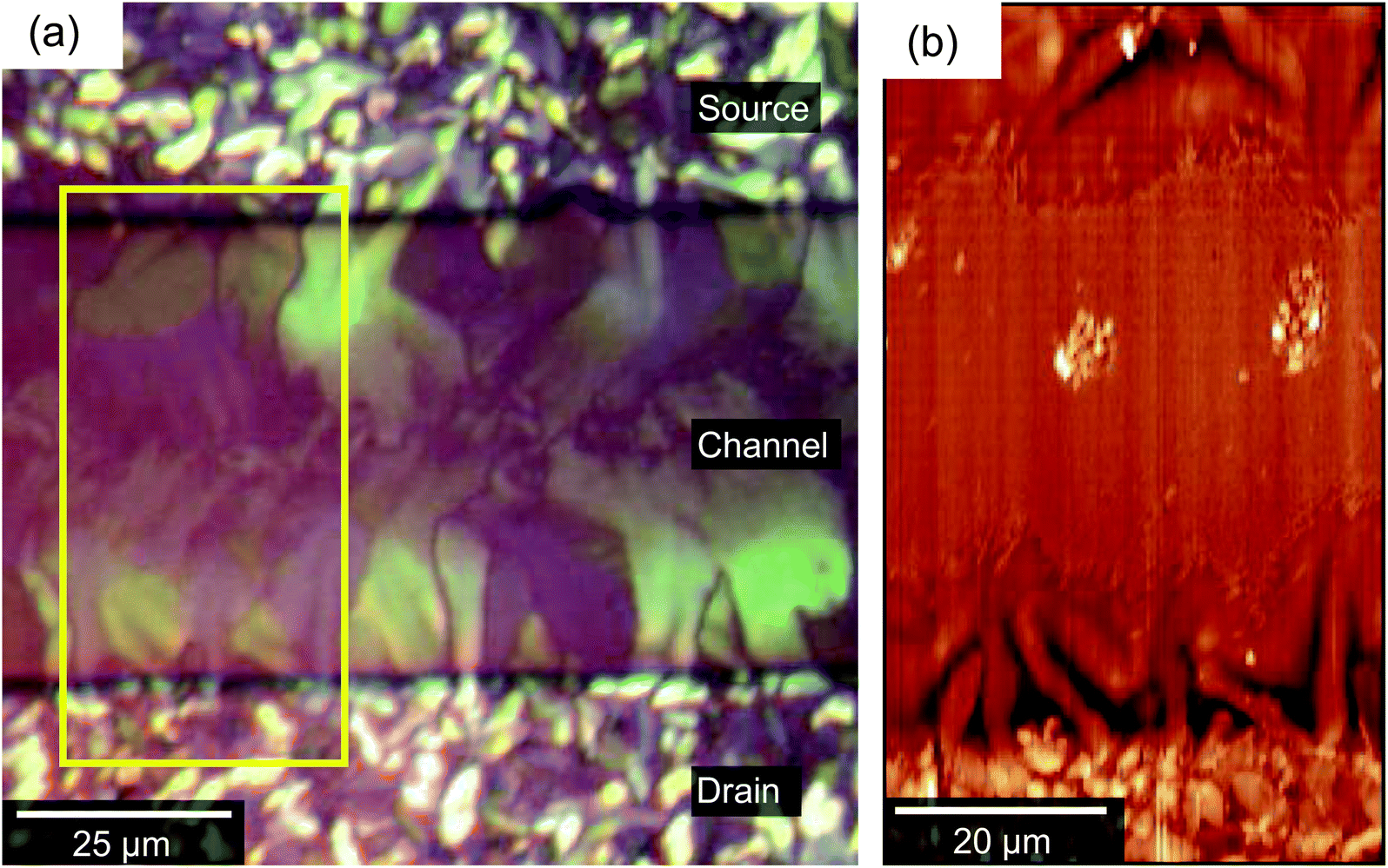 | ||
| Fig. 8 (a) An optical micrograph of the channel region of a poorly-performing device. A dark, less birefringent band along the centre of the channel can be seen. (b) The corresponding AFM image showing that the dark band in the POM image is composed of regions (C) and (D) of Fig. 4. | ||
Conclusions
In summary we have fabricated small molecule/polymer blend OFET devices with excellent device-to-device uniformity, exhibiting saturation mobilities that are competitive with amorphous silicon devices. Additionally, we have performed a detailed structural characterisation of BGBC OFET devices employing a polymeric dielectric and have developed structure–function relations. We have thus developed a first descriptive model of the nucleation and growth of diF-TES-ADT, leading to the establishment of four structurally distinct crystalline regimes. These regimes arise due to ‘natural lengthscales’ of growth that are imposed by five major kinetic parameters: the rate of heterogeneous nucleation on the electrodes; the rate of crystal growth; the rate of solvent evaporation; the rate of OSC diffusion in the solvent; and the rate of homonucleation. We anticipate that it should be possible to tailor these relative kinetics in order to match the characteristic length-scales of petal growth, etc. to a preferred device channel length and thereby optimise performance. Finally, we note that the methodology presented here and a comprehensive use of scanning probe microscopies – particularly the visualisation of potential drops at grain boundaries using KPM – are remarkably powerful for characterising OFET structure and function, which is of utmost importance to the advancement of OFET devices, such as the dinapthothienothiophene (DNTT) BGBC devices that have recently attracted attention.49Acknowledgements
This research was supported by the Engineering and Physical Sciences Research Council (EPSRC) through a doctoral training grant and grant EP/I00419X/1.Notes and references
- Q.-D. Ling, D.-J. Liaw, C. Zhu, D. S.-H. Chan, E.-T. Kang and K.-G. Neoh, Prog. Polym. Sci., 2008, 33, 917–978 CrossRef CAS PubMed.
- C. Huang, J. E. West and H. E. Katz, Adv. Funct. Mater., 2007, 17, 142–153 CrossRef CAS.
- B. Crone, A. Dodabalapur, A. Gelperin, L. Torsi, H. E. Katz, A. J. Lovinger and Z. Bao, Appl. Phys. Lett., 2001, 78, 2229–2231 CrossRef CAS.
- S. Subramanian, S. K. Park, S. R. Parkin, V. Podzorov, T. N. Jackson and J. E. Anthony, J. Am. Chem. Soc., 2008, 130, 2706–2707 CrossRef CAS PubMed.
- C. D. Dimitrakopoulos and P. R. L. Malenfant, Adv. Mater., 2002, 14, 99–117 CrossRef CAS.
- J. A. Lim, H. S. Lee, W. H. Lee and K. Cho, Adv. Funct. Mater., 2009, 19, 1515–1525 CrossRef CAS.
- H. Sirringhaus, N. Tessler and R. H. Friend, Science, 1998, 280, 1741–1744 CrossRef CAS.
- J. Kang, N. Shin, D. Y. Jang, V. M. Prabhu and D. Y. Yoon, J. Am. Chem. Soc., 2008, 130, 12273–12275 CrossRef CAS PubMed.
- S. Y. Cho, J. M. Ko, J.-Y. Jung, J. Y. Lee, D. H. Choi and C. Lee, Org. Electron., 2012, 13, 1329–1339 CrossRef CAS PubMed.
- R. Hamilton, J. Smith, S. Ogier, M. Heeney, J. E. Anthony, I. McCulloch, J. Veres, D. D. C. Bradley and T. D. Anthopoulos, Adv. Mater., 2009, 21, 1166–1171 CrossRef CAS.
- J. Smith, R. Hamilton, Y. Qi, A. Kahn, D. D. C. Bradley, M. Heeney, I. McCulloch and T. D. Anthopoulos, Adv. Funct. Mater., 2010, 20, 2330–2337 CrossRef CAS.
- O. D. Jurchescu, S. Subramanian, R. J. Kline, S. D. Hudson, J. E. Anthony, T. N. Jackson and D. J. Gundlach, Chem. Mater., 2008, 20, 6733–6737 CrossRef CAS.
- J. Smith, W. Zhang, R. Sougrat, K. Zhao, R. Li, D. Cha, A. Amassian, M. Heeney, I. McCulloch and T. D. Anthopoulos, Adv. Mater., 2012, 24, 2441–2446 CrossRef CAS PubMed.
- M. Gruber, E. Zojer, F. Schürrer and K. Zojer, Adv. Funct. Mater., 2013, 23, 2941–2952 CrossRef CAS.
- D. J. Gundlach, J. E. Royer, S. K. Park, S. Subramanian, O. D. Jurchescu, B. H. Hamadani, A. J. Moad, R. J. Kline, L. C. Teague, O. Kirillov, C. A. Richter, J. G. Kushmerick, L. J. Richter, S. R. Parkin, T. N. Jackson and J. E. Anthony, Nat. Mater., 2008, 7, 216–221 CrossRef CAS PubMed.
- J. Veres, S. D. Ogier, S. W. Leeming, D. C. Cupertino and S. Mohialdin Khaffaf, Adv. Funct. Mater., 2003, 13, 199–204 CrossRef CAS.
- A. L. Deman, M. Erouel, D. Lallemand, M. Phaner-Goutorbe, P. Lang and J. Tardy, J. Non-Cryst. Sol., 2008, 354, 1598–1607 CrossRef CAS PubMed.
- J. Smith, M. Heeney, I. McCulloch, J. N. Malik, N. Stingelin, D. D. C. Bradley and T. D. Anthopoulos, Org. Electron., 2011, 12, 143–147 CrossRef CAS PubMed.
- M. Lada, M. J. Starink, M. Carrasco, L. Chen, P. Miskiewicz, P. Brookes, M. Obarowska and D. C. Smith, J. Mater. Chem., 2011, 21, 11232–11238 RSC.
- G. Horowitz, R. Hajlaoui, H. Bouchriha, R. Bourguiga and M. Hajlaoui, Adv. Mater., 1998, 10, 923–927 CrossRef CAS.
- S. Locci, M. Morana, E. Orgiu, A. Bonfiglio and P. Lugli, IEEE Trans. Electron Devices, 2008, 55, 2561–2567 CrossRef.
- W. Wang, D. Ma, S. Pan and Y. Yang, Appl. Phys. Lett., 2012, 101, 033303 CrossRef.
- R. Li, J. W. Ward, D.-M. Smilgies, M. M. Payne, J. E. Anthony, O. D. Jurchescu and A. Amassian, Adv. Mater., 2012, 24, 5553–5558 CrossRef CAS PubMed.
- R. J. Kline, S. D. Hudson, X. Zhang, D. J. Gundlach, A. J. Moad, O. D. Jurchescu, T. N. Jackson, S. Subramanian, J. E. Anthony, M. F. Toney and L. J. Richter, Chem. Mater., 2011, 23, 1194–1203 CrossRef CAS.
- Y.-H. Kim, J. E. Anthony and S. K. Park, Org. Electron., 2012, 13, 1152–1157 CrossRef CAS PubMed.
- H. Sirringhaus, T. Sakanoue and J.-F. Chang, Phys. Status Solidi B, 2012, 249, 1655–1676 CrossRef CAS.
- O. D. Jurchescu, B. H. Hamadani, H. D. Xiong, S. K. Park, S. Subramanian, N. M. Zimmerman, J. E. Anthony, T. N. Jackson and D. J. Gundlach, Appl. Phys. Lett., 2008, 92, 132103 CrossRef.
- L. Gránásy, T. Pusztai, G. Tegze, J. A. Warren and J. F. Douglas, Phys. Rev. E: Stat., Nonlinear, Soft Matter Phys., 2005, 72, 011605 CrossRef.
- H. Kang, N.-S. Lee, E. Ito, M. Hara and J. Noh, Langmuir, 2010, 26, 2983–2985 CrossRef CAS PubMed.
- M. C. Schalnat and J. E. Pemberton, Langmuir, 2010, 26, 11862–11869 CrossRef CAS PubMed.
- T. Minari, M. Kano, T. Miyadera, S.-D. Wang, Y. Aoyagi, M. Seto, T. Nemoto, S. Isoda and K. Tsukagoshi, Appl. Phys. Lett., 2008, 92, 173301 CrossRef.
- Z. Jia, V. W. Lee, I. Kymissis, L. Floreano, A. Verdini, A. Cossaro and A. Morgante, Phys. Rev. B: Condens. Matter Mater. Phys., 2010, 82, 125457 CrossRef.
- W. Chen, X. Y. Gao, D. C. Qi, S. Chen, Z. K. Chen and A. T. S. Wee, Adv. Funct. Mater., 2007, 17, 1339–1344 CrossRef CAS.
- K. C. Dickey, J. E. Anthony and Y. L. Loo, Adv. Mater., 2006, 18, 1721–1726 CrossRef CAS.
- I. H. Campbell, J. D. Kress, R. L. Martin, D. L. Smith, N. N. Barashkov and J. P. Ferraris, Appl. Phys. Lett., 1997, 71, 3528–3530 CrossRef CAS.
- N. Shin, J. Kang, L. J. Richter, V. M. Prabhu, R. J. Kline, D. A. Fischer, D. M. DeLongchamp, M. F. Toney, S. K. Satija, D. J. Gundlach, B. Purushothaman, J. E. Anthony and D. Y. Yoon, Adv. Funct. Mater., 2013, 23, 366–376 CrossRef CAS.
- J. Chen, C. K. Tee, M. Shtein, J. Anthony and D. C. Martin, J. Appl. Phys., 2008, 103, 114513 CrossRef.
- A. D. Carlo, F. Piacenza, A. Bolognesi, B. Stadlober and H. Maresch, Appl. Phys. Lett., 2005, 86, 263501 CrossRef.
- L. C. Teague, B. H. Hamadani, O. D. Jurchescu, S. Subramanian, J. E. Anthony, T. N. Jackson, C. A. Richter, D. J. Gundlach and J. G. Kushmerick, Adv. Mater., 2008, 20, 4513–4516 CrossRef CAS.
- L. Burgi, H. Sirringhaus and R. H. Friend, Appl. Phys. Lett., 2002, 80, 2913–2915 CrossRef CAS.
- S. Hunter and T. D. Anthopoulos, Adv. Mater., 2013, 25, 4320–4326 CrossRef CAS PubMed.
- J. Chen, C. K. Tee, M. Shtein, D. C. Martin and J. Anthony, Org. Electron., 2009, 10, 696–703 CrossRef CAS PubMed.
- C. F. Matta, N. Castillo and R. J. Boyd, J. Phys. Chem. A, 2005, 109, 3669–3681 CrossRef CAS PubMed.
- J. Rivnay, S. C. B. Mannsfeld, C. E. Miller, A. Salleo and M. F. Toney, Chem. Rev., 2012, 112, 5488–5519 CrossRef CAS PubMed.
- S. S. Lee, S. B. Tang, D.-M. Smilgies, A. R. Woll, M. A. Loth, J. M. Mativetsky, J. E. Anthony and Y.-L. Loo, Adv. Mater., 2012, 24, 2692–2698 CrossRef CAS PubMed.
- T. Ohe, M. Kuribayashi, R. Yasuda, A. Tsuboi, K. Nomoto, K. Satori, M. Itabashi and J. Kasahara, Appl. Phys. Lett., 2008, 93, 053303 CrossRef.
- J. Smith, R. Hamilton, M. Heeney, D. M. de Leeuw, E. Cantatore, J. E. Anthony, I. McCulloch, D. D. C. Bradley and T. D. Anthopoulos, Appl. Phys. Lett., 2008, 93, 253301–253303 CrossRef.
- W. H. Lee, D. Kwak, J. E. Anthony, H. S. Lee, H. H. Choi, D. H. Kim, S. G. Lee and K. Cho, Adv. Funct. Mater., 2012, 22, 267–281 CrossRef CAS.
- M. J. Kang, I. Doi, H. Mori, E. Miyazaki, K. Takimiya, M. Ikeda and H. Kuwabara, Adv. Mater., 2011, 23, 1222–1225 CrossRef CAS PubMed.
Footnote |
| † Electronic supplementary information (ESI) available: Additional morphological characterisations and TEM data. See DOI: 10.1039/c3tc31783h |
| This journal is © The Royal Society of Chemistry 2014 |