 Open Access Article
 This Open Access Article is licensed under a Creative Commons Attribution-Non Commercial 3.0 Unported Licence
Large area uniform deposition of silver nanoparticles through bio-inspired polydopamine coating on silicon nanowire arrays for practical SERS applications
Merve Selen
Akin
a,
Mehmet
Yilmaz
a,
Esra
Babur
a,
Betul
Ozdemir
a,
Hakan
Erdogan
a,
Ugur
Tamer
b and
Gokhan
Demirel
*a
aBio-Inspired Materials Research Laboratory (BIMREL), Department of Chemistry, Gazi University, 06500 Ankara, Turkey. E-mail: nanobiotechnology@gmail.com
bDepartment of Analytical Chemistry, Faculty of Pharmacy, Gazi University, 06330 Ankara, Turkey
First published on 23rd May 2014
Abstract
Despite the significant progress, the controlled deposition of nanoparticles onto the support materials having 3-D nano-morphologies is still facing challenges due to the limited diffusion of metal ions into the nanostructures and uncontrolled aggregation of nanoparticles. In this study, a simple yet versatile alternative is demonstrated to control the silver nanoparticle (AgNP) density and morphology onto the 3-D silicon nanowire (SiNW) arrays based on bio-inspired polydopamine (PDOP) coating and electroless plating approaches for practical Surface-Enhanced Raman Spectroscopy (SERS) applications. In order to control silver deposition and its morphology and to optimize the SERS performance of AgNP decorated SiNW arrays, the effect of some key experimental parameters including SiNW length and morphology, silver reduction time and PDOP thickness are investigated in detail. The optimized samples demonstrate remarkable surface-enhancement ability in Raman signals with high reproducibility (lower than ∼10% spot-to-spot and sample-to-sample). Interestingly, it is found that PDOP coating not only serves as a reducing agent for the deposition of AgNPs on SiNW arrays in a controlled manner, but also contributes to the observed SERS enhancements in terms of improving photon scattering and promoting electron transfer processes due to its organic semiconductor nature.
1. Introduction
Surface-Enhanced Raman Spectroscopy (SERS) has attracted increasing interest as a powerful analytical tool for the detection of chemical and biological molecules since its discovery.1–5 In SERS studies, the enhancement of Raman signals fundamentally stems from the electromagnetic field in close vicinity of nanostructures with plasmonic features on a surface.3 In this context, to gain the unique SERS spectra of target molecules at trace amounts, a series of innovative strategies have been proposed to develop a reliable, sensitive, and selective SERS-based sensing platform.2,6 Although the employment of noble metal nanoparticles such as gold and silver on solid substrates is undoubtedly a simple and facile method for creating such platforms, their uncontrolled aggregation leads to a poor reproducibility and discrepancy in the resulting SERS signals which limit their applications.7,8 Alternatively, to eliminate the uncontrolled aggregation and to achieve spatial arrangement of nanostructures, much more sophisticated nanofabrication techniques such as oblique angle deposition,9 nanosphere lithography,10 electron beam lithography,11 and focused ion beam milling12 are currently available. The substrates prepared by these techniques have provided large Raman enhancement ability and good SERS reproducibility due to multiple hot spot generations, cavity resonances, and propagation of surface plasmon resonances (SPRs).13,14 On the other hand, these techniques are too technologically demanding and quite expensive in the fabrication of large quantities of substrates.15According to recent theoretical and experimental reports, precise control of the size and uniformity of noble metal nanoparticles on surfaces with 3-D morphology is a key issue in fabrication of SERS based sensor platforms.16,17 To address this issue, many methods including vapor phase deposition, sputtering, electrochemical plating and immobilization have been investigated.18–23 For example, Zhang et al. reported the SERS performance of silver-coated silicon nanowire (SiNW) arrays in terms of enhancement ability, stability, and reproducibility.15 Although the optimized silver-coated SiNW arrays exhibited good SERS performances, the fabrication procedure of this platform requires multistep and complicated procedures and unwanted impurities related to use of chemicals and solvents may also pose a serious deterrent to sensitive and selective detection. Besides, there is no data on the morphology change of the deposited silver over time and its effect on the SERS efficiency. In another study, silver nanoparticles (AgNPs) were directly grown on SiNWs through galvanic redox reaction without any organic contamination.24 Despite the easiness of the proposed method to fabricate the SERS-active substrate, the uncontrolled growth of AgNPs with broad size distribution as well as tendency of AgNPs to grow at the tips of SiNWs due to limited diffusion of silver are major drawbacks that limit the practical application of SERS. In a similar way, Galopin et al. fabricated SiNWs through the vapor-liquid-solid growth mechanism and AgNPs were then deposited by an electroless deposition technique.25 Non-uniform silver deposition with different morphologies was observed on the upper and lower parts of each array probably due to diffusion limitation and crossing and contact between SiNWs. These reports clearly show that simple but effective new strategies for the fabrication of nanoparticle decorated 3-D nano-morphologies in a controlled manner are still needed for SERS applications in order to reach their full potential.
In this study, we proposed a simple and versatile method to control the size and uniformity of AgNPs on vertically aligned SiNW arrays as an ideal SERS platform through polydopamine (PDOP) coating. The main advantage of PDOP is, as inspired from mussels, the ability to be deposited on almost all types of inorganic and organic substrates with controllable film thickness and durable stability as well as excellent biocompatibility.26,27 The vast functional groups of PDOP including catechol, amine and imine also serve as both the reducing agent toward metal ions and the anchor for grown metal nanoparticles neither using additional reductants nor metallic seed particles.26 Moreover, the PDOP coating will provide remarkable contribution for SERS enhancement in some respects due to its unique organic semiconductor nature.26 In order to control silver deposition and its morphology and to optimize the SERS performance of AgNP decorated SiNW arrays, we investigated the effect of some experimental parameters such as the SiNW length and morphology, silver reduction time and PDOP thickness in detail. Our proposed system resulted in well-controlled and uniform deposition of AgNPs on SiNWs with remarkable SERS performance in terms of enhancement, simplicity and reproducibility.
2. Experimental section
Fabrication of silicon nanowire arrays
The silicon nanowire arrays were prepared via a metal-assisted chemical etching technique as reported elsewhere.28–31 Briefly, silicon wafers with (001) crystallographic orientations and 1–10 Ω cm resistivity were first sonicated in ethanol and acetone for 5 min, respectively. They were then transferred into a mixture of H2SO4 and H2O2 having a volume ratio of 3![[thin space (1/6-em)]](https://www.rsc.org/images/entities/char_2009.gif) :1 at 70 °C. After 60 min, the wafers were removed, washed with water, and dried with N2 gas. Finally, they were treated in a UV/ozone chamber for 10 min. Following the pre-cleaning steps, the samples were immersed into HF solution (1 min) and immediately transferred to a Teflon baker containing 0.02 M of AgNO3 and 4.6 M of HF (1:1 v/v) for 1 min. Finally, silver nanoparticle covered wafers were dipped into an etching solution (HF (4.6 M):H2O2 (30%), 10:1 v/v) at room temperature for various durations (10–120 min). After a certain time, samples were removed and rinsed with water and HNO3 to remove Ag dendrites which were formed as by-products.
:1 at 70 °C. After 60 min, the wafers were removed, washed with water, and dried with N2 gas. Finally, they were treated in a UV/ozone chamber for 10 min. Following the pre-cleaning steps, the samples were immersed into HF solution (1 min) and immediately transferred to a Teflon baker containing 0.02 M of AgNO3 and 4.6 M of HF (1:1 v/v) for 1 min. Finally, silver nanoparticle covered wafers were dipped into an etching solution (HF (4.6 M):H2O2 (30%), 10:1 v/v) at room temperature for various durations (10–120 min). After a certain time, samples were removed and rinsed with water and HNO3 to remove Ag dendrites which were formed as by-products.
Silver nanoparticle synthesis on SiNW arrays
For silver nanoparticle synthesis, the as-prepared SiNW arrays were first coated with the PDOP film. Typically, the SiNW arrays were immersed into a dopamine solution (2 mg mL−1 in 10 mM Tris buffer, pH 8.5) at room temperature for various durations (1–24 h). The samples were then rinsed with water and dried with N2 gas. Finally, PDOP coated SiNWs were treated with an ionic silver solution (50 mM AgNO3 in double distilled water) for varying reduction time periods (3–24 h) to grow AgNPs along the PDOP coated SiNWs.Characterization
The morphologies of fabricated samples were characterized by using a Quanta 400F field-emission scanning electron microscope (FE-SEM) with an acceleration voltage of 10 kV. The thicknesses of PDOP films on the SiNWs, which were measured indirectly using a smooth silicon wafer placed next to the SiNW samples during PDOP deposition, were analyzed with a variable-angle spectroscopic-phase-modulated ellipsometer (UVISEL, Jobin Yvon-Horiba). In the layer thickness analysis, a four-phase model consisting of silicon substrate/SiO2/overlayer/air was assumed. All thickness values given in the text are the averages of at least three measurements taken at three different locations on each sample surface.In SERS studies, a Delta Nu Examiner Raman Microscopy system equipped with a 785 nm laser source, a motorized microscope stage sample holder, and a cooled charge-coupled device (CCD) detector was employed in the range of 200–2000 cm−1. The related Raman instrument parameters were as follows: 20× objective, 30 μm spot size, 30 s acquisition time, and 150 mW laser power. For all measurements, baseline correction was performed. To evaluate the SERS performance, methylene blue (MB) was selected as the Raman reporter molecule and 3 μL of 1 mM aqueous solution of MB was dropped onto the Ag nanoparticle decorated SiNW arrays and kept in a hood until dry. The drying procedure led to coin-shaped Raman sample sizes of 4 ± 1 mm onto the sample surfaces. For each sample, at least ten Raman spectra were collected from the different spots of the substrate to determine the reproducibility and homogeneity.
3. Results and discussion
In the first part of this study, we fabricated SiNW arrays having varying morphologies through a well-known metal-assisted chemical etching28–31 method by controlling the etching time period. We kept constant the etching temperature for all experiments at 25 °C and set the etching time at 10 min, 30 min, 60 min and 120 min, respectively. Typical cross-sectional and top-view SEM images of the fabricated samples are depicted in Fig. 1. It can be clearly seen that the SiNWs are vertical to the Si wafer surface with varying lengths as desired. The diameter and length of the fabricated SiNWs were measured by employing freeware IMAGEJ software. When the etching time reached 10 min, the surface of the silicon wafer was fully covered by many uniformly generated and freestanding SiNWs with a length of 8.2 ± 0.8 μm (Fig. 1a and e). As the etching time period increased, the SiNWs gradually elongated and numerous sharp tips emerged. The length of SiNWs were determined to be 24.3 ± 1.9 μm, 37.5 ± 2.7 μm, and 62.5 ± 3.3 μm for the cases of 30, 60, and 120 min of etching time periods, respectively (Fig. 1b–d). For the long etching process (i.e., 60 and 120 min), the interconnection of SiNWs on top of them can easily be observed through the top-view SEM images (Fig. 1g and h). Tangled SiNWs with a certain length are held together in bundles due to effective surface tensional forces during the drying process and subsequently the van der Waals forces hold SiNWs together.32,33 In addition to these, it is observed that the as-prepared SiNWs have almost the same diameter throughout the length of the nanowire independent of etching time periods. The diameters of SiNWs are in the range of 50–300 nm (Fig. 1a–d). | ||
| Fig. 1 Cross-sectional and top-view SEM images of vertically aligned SiNW arrays for (a and e) 10 min, (b and f) 30 min, (c and g) 60 min, and (d and h) 120 min of etching time periods. | ||
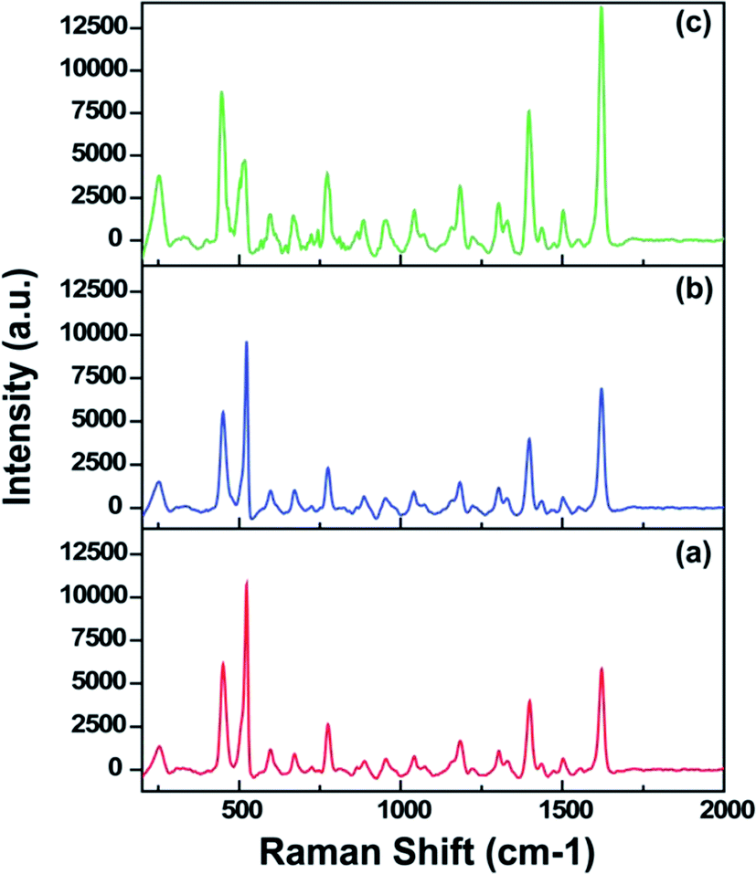
To evaluate the effect of surface morphologies of fabricated SiNW arrays on SERS performances, a thin layer of PDOP (∼7 nm) was first coated on the SiNW surfaces by controlling the oxidative polymerization time of dopamine, and silver nanoparticles were subsequently grown in situ on the PDOP coated SiNWs into the 50 mM AgNO3 solution for 24 h. For all SERS measurements, methylene blue (MB) was used as a Raman reporter. Typically, 3 μL of MB solution (1 mM) was dropped onto the sample surfaces and kept in a hood until dry. The drying process led to coin-shaped Raman sample sizes of 4 ± 1 mm. Fig. 2 reveals the SERS spectra of MB molecules obtained from these samples. All collected spectra are precise and have acceptable signal-to-noise ratios consistent with the earlier reports for MB.9,34,35 For all cases, the most prominent peaks in the spectra of MB are the ring stretch (ν(C–C)) at ∼1621 cm−1, symmetric and asymmetric C–N stretches (νsym(C–N) and νasym(C–N)) at ∼1398 and ∼1436 cm−1, respectively, and the C–N–C skeletal deformation mode (δ(C–N–C)) at ∼449 cm−1. For a short etching time period (10 min), Raman spectra with a low SERS signal intensity was detected (Fig. 2a) possibly due to the dense silver nanoparticle formation onto samples, which led to the disappearance of the unique features of SiNW arrays such as high-aspect ratio, sharp vertices, and interwire coupling which is disadvantageous for SERS enhancement.15 Increasing the etching time from 10 min to 30 min resulted in a highly remarkable (six-fold) increment in the SERS signal intensity according to a prominent peak at around 1620 cm−1. This result is somewhat expected. The interconnection on SiNWs with the forest-like, highly tangled and uniformly closely packed structure proved to be an ideal SERS substrate (Fig. 1b, f and 2d). Further increment in the etching time (60 and 120 min) led to Raman signals with lower intensity (Fig. 2c and b) possibly due to the discrete and bundled morphologies of SiNWs (Fig. 1g and h). These morphologies might have created some dead points over the Raman spot size and lowered the SERS performance of SiNW arrays. To quantify and compare the SERS performance of Ag nanoparticle decorated samples (Ag@SiNWs), we also calculated the SERS enhancement factors (EF) by applying the following equation using the Raman intensity peak of MB at around 1620 cm−1;
| EF = (NBulk × IAgNP@SiNW)/(NAgNP@SiNW × IBulk) | (1) |
 | ||
| Fig. 2 SERS spectra of MB on the AgNP@SiNW arrays fabricated at different etching time periods: (a) 10 min, (b) 120 min, (c) 60 min and, (d) 30 min. | ||
Uniform deposition and distribution of plasmonic noble metal nanostructures such as AgNPs on the SiNW surfaces is essential to acquire reproducible Raman spectra with high efficiency. Silver, which provides a higher SERS enhancement efficiency in the visible light wavelength region compared to gold or others, is mostly used as the metal to incorporate in 3-D nanostructured samples.15,36 To investigate the morphology and distribution of AgNPs on SiNW arrays and their relevant SERS performances, the AgNPs were grown in-situ on the PDOP coated SiNW samples at varying reduction time periods (3–24 h). In the case of AgNP formation, the catechol groups in the PDOP film are mainly responsible for the in situ formation of AgNPs due to their ability to release electrons when oxidized into the corresponding quinone groups which trigger reduction processes of silver cations to silver nanoparticles.26 For all samples, which were used for the AgNP deposition, we fixed the etching time for SiNW fabrication at 30 min and PDOP thickness on SiNWs at ∼7 nm. Fig. 3 shows the cross-sectional SEM images of AgNP deposited SiNW arrays at varying reduction time periods. In the case of 3 h reduction time, lower particle density and higher size distribution for deposited AgNPs on SiNWs was observed compared with the other situations (Fig. 3a and d). The size distribution of AgNPs is in the range of 12–70 nm with an average size of 30 nm. For this case, the AgNPs are highly separated from each other. Consequently, it is not surprising to observe the lowest SERS enhancement of this set with 1.5 × 10⁶ EF value (Fig. 4a). We perceive that the resulting SERS enhancement may be attributed to the underlying substrate. Since the 3-D SiNW arrays have a large surface area and a huge amount of surface electrons, the incident electromagnetic wave may effectively entrap and lead to further enhancement of surface plasmon resonance of AgNPs on SiNWs.24 Moreover, the PDOP coating on SiNWs may be another contributor for SERS enhancement. Recent reports have shown that PDOP is an organic semiconductor and it has a broad range adsorption capability that leads to the generation of electrons.26 Therefore, a thin layer of PDOP coating may promote the electron transfer to AgNPs resulting to enhancement of surface plasmon resonance. Increasing the reduction time period from 3 h to 12 h resulted in a remarkable change in morphology and size as well as surface density of AgNPs. The AgNPs are in the range of 20–80 nm with an average size of 60 nm (Fig. 3b and e). Since the size and surface density of AgNPs increased, the nanoparticles get closer and closer. Garcia-Vidal and Pendry have proposed a model that can be applied to our case to quantitatively measure the electromagnetic interaction between adjacent metallic objects.37 In their model, they reported that the average enhancement increases from 103 for “isolated” particles to a maximum of 106 for the case d = 2R where the particles are in direct contact. In this equation, d is the distance between the centers of two adjacent particles and 2R is also the particle diameter.37 For the case of 12 h reduction time period, since d is quite lower than 2R (see Fig. 3e), it is reasonable to expect huge local electric field and resultant SERS enhancement. The representative Raman spectra of related SERS substrate (Fig. 4b) showed a higher Raman intensity with 2.2 × 10⁶ EF value. Further increment in reduction time (24 h) led to dramatic change in the surface morphology of AgNPs on SiNWs. Fig. 3c and f depict the disappearance of discrete AgNPs and merge of nanoparticles due to excessive growth by time. Highly porous and densely packed nature of this substrate had an enormously higher SERS performance (Fig. 4c) with a calculated EF value of 3.6 × 10⁶ compared with the other situations. Garcia-Vidal and Pendry have also analyzed the quantitative dependence of the localized plasmon mode on the surface roughness for the case of d ≤ 2R and observed that the enhancement effect diminishes with decreasing roughness.37 In our case, the highly dense and porous morphology of AgNPs on the SiNWs exhibited the highest Raman efficiency.
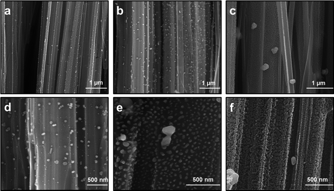 | ||
| Fig. 3 SEM images of AgNP deposited SiNWs for (a and d) 3 h, (b and e) 12 h, and (c and f) 24 h of silver ion reduction time. Each sample was etched for 30 min and coated with the same thickness of PDOP (∼7 nm). | ||
 | ||
| Fig. 4 SERS spectra of MB on the AgNP@SiNW arrays fabricated at different silver ion reduction time periods: (a) 3 h, (b) 12 h, and (c) 24 h. | ||
The PDOP coating based on oxidative polymerization of dopamine molecules under alkaline conditions with oxygen as the oxidant is a simple, very effective and material independent route. By this way, various materials either organic or inorganic may easily be modified in controlled a manner.26,27 Since the pioneering work by Messersmith group,27 PDOP coating has been widely investigated in a variety of fields. However, the polymerization mechanism of dopamine is still not fully understood due to the complex redox process and the generation of a series of intermediates during the reaction processes. According to previous reports,26 dopamine is first oxidized to dopaminequinone and subsequently transformed to leukodopaminechrome through intramolecular cyclization under alkaline conditions. Afterwards, leukodopaminechrome suffers from oxidization and rearrangement to form 5,6-dihydroxyindole, which is easily further oxidized to 5,6-indolequinone.26 These two molecules formed multiple isomers of dimers and higher oligomers which may self-assemble further into the cross-linked polydopamine. Meanwhile, it is also found that a considerable amount of unpolymerized dopamine also formed a self-assembled complex with its oxidative product, 5,6-dihydroxyindole.38 Therefore, PDOP may be considered to be an aggregate of monomers similar to other synthetic or biological polymers.38 One of the remarkable advantages of PDOP coating is to reduce metal ions into metal nanoparticles. In this context, neither additional reducing agents nor metallic seed particles are required. Moreover, recent reports have demonstrated that PDOP has unique optical and electrical properties which are needed to keep in mind in SERS investigation. For these reasons, we evaluated the PDOP film thickness on the SERS performances of proposed platforms. In this set of experiments, we fixed the etching time for SiNW fabrication at 30 min and reduction time for silver ions at 24 h. By changing PDOP polymerization time periods (1–24 h), PDOP thickness deposited on SiNWs have been manipulated. The thicknesses of deposited PDOP films on SiNWs were measured indirectly using a smooth silicon wafer placed next to the samples during polymerization. As expected, thicknesses of the PDOP layer increased when the polymerization time period was increased. The PDOP thicknesses were found to be 2.2 ± 0.86 nm for 1 h, 6.78 ± 1.21 nm for 3 h, 11.8 ± 1.03 nm for 6 h, 22.6 nm ± 2.17 nm for 12 h, and 38.3 ± 2.41 nm for 24 h of polymerization time, respectively. Bernsmann et al. and Lee et al. independently showed that the maximum thickness of the PDOP film in a single reaction step is about 50 nm and further increasing the concentration of the dopamine monomer or prolonging the reaction time does not help to increase the thickness of the film.27,39
Fig. 5 compares the SERS spectra of MB molecules obtained from the above mentioned samples. In a short polymerization time period (1 h), a quite reasonable Raman spectrum with high intensity was obtained (Fig. 5a). The SERS intensity increased with the PDOP polymerization time from 1 h to 3 h, and reaches its maximum (Fig. 5b). Interestingly, increasing PDOP polymerization time periods from 3 h to 6 h led to a dramatic decrease in intensity of the Raman signal. The same inclination was observed in further polymerization times of PDOP (Fig. 5c–e). This issue may be attributed to the thickness of PDOP. For the cases of 1 h and 3 h of polymerization time periods, the chemical interactions between the AgNPs and the PDOP layer might have enhanced the scattering process. The electrons in the AgNP-conducting band are excited to the lowest unoccupied molecular orbital of PDOP by incident laser, and this unstable state relaxes through the jumping back of the electrons. Subsequently, a dipole between the AgNP and PDOP as well as adsorbate MB is formed as a result of this process. These surface dipoles may couple, resonate and transmit due to near field effect.24 The resultant dipoles may improve the scattering process and lead to an increase in the SERS intensity. Additionally, electron transfer to AgNPs from the PDOP layer due to its broad band adsorption capability may contribute to enhancement of the surface plasmon resonance of AgNPs as well as SERS performance.26 However, for the thicker PDOP layer (6–24 h), contributions of the above mentioned issues remain limited and may not improve the SERS intensity efficiently. In these cases, we assume that high density molecular stacking and un-uniform molecular arrangement of the PDOP film prevent the electronic movement and scattering. However, theoretical modeling and more detailed experiments are still needed to better understand this phenomenon.
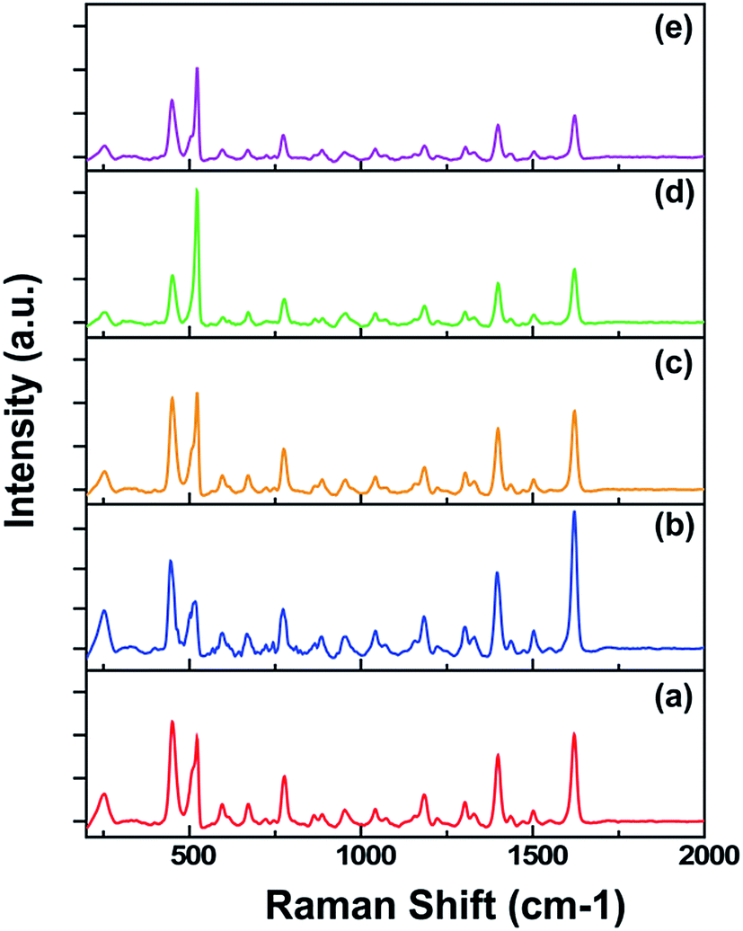 | ||
| Fig. 5 SERS spectra of MB on the AgNP@SiNW arrays fabricated at different polymerization times of PDOP: (a) 1 h, (b) 3 h, (c) 6 h, (D) 12 h, and (e) 24 h. | ||
It is well-known that the poor reproducibility of Raman signals in SERS studies is the main obstacle that should be considered to prove the proposed system as an ideal SERS substrate. To evaluate the reproducibility of our substrate, we collected SERS spectra of MB molecules from 50 randomly selected positions on the optimized AgNP@SiNW arrays under identical experimental conditions (Fig. 6). It is clear that for all runs, Raman spectra with high reproducibility efficiency were determined. To clarify and quantify the reproducibility, we calculated the relative standard deviation (RSD) for the spectra given in Fig. 6. Table 1 shows the RSD values in intensity changes and position shift of prominent Raman peaks. According to RSD values and peak positions, we can conclude that RSD values below 0.21 revealed a good reproducibility across the entire area of the optimized AgNP@SiNW arrays. One exception is the peak at around 521 cm−1. This peak is originated from the nature of SiNW arrays.40
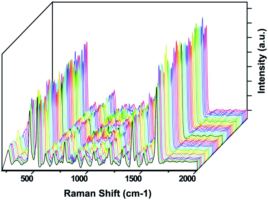 | ||
| Fig. 6 Reproducibility of SERS spectra of MB collected on the randomly selected 50 spots of the optimized AgNP@SiNW arrays. | ||
| Peak Position (cm−1) | 1621 ± 0.5 | 1398 ± 0.8 | 1303 ± 0.5 | 1183 ± 0.8 | 774 ± 0.6 | 521 ± 1 | 449 ± 0.8 |
|---|---|---|---|---|---|---|---|
| RSD value | 0.08 | 0.1 | 0.09 | 0.09 | 0.13 | 0.21 | 0.07 |
4. Conclusion
In this paper, we reported a simple yet very effective way to control the size and density of silver nanoparticles on 3-D SiNW arrays based on bio-inspired PDOP coating for practical SERS applications. The optimized AgNP decorated SiNW arrays exhibit remarkable surface-enhancement ability in Raman signals with high reproducibility (lower than ∼10% spot-to-spot and sample-to-sample). Interestingly, it is found that the PDOP coating not only serves as a reducing agent for the deposition of AgNPs on SiNW arrays, but also contributes to the SERS enhancement in terms of improving photon scattering and promoting electron transfer processes due to its organic semiconductor nature. Although there are still many challenges ahead related to SERS, the present concept can be regarded as an important step towards the fabrication of an ideal SERS platform and may open up intriguing opportunities for practical SERS applications.Acknowledgements
This work was supported by the Scientific and Technological Research Council (TUBITAK) grant number 111M237. M. Y. is supported by TUBITAK BIDEB fellowship. M. S. A. and M. Y. contributed equally to this work.References
- M. G. Albrecht and J. A. Creighton, J. Am. Chem. Soc., 1977, 99, 5215 CrossRef CAS.
- M. Moskovits, J. Raman Spectrosc., 2005, 36, 485 CrossRef CAS.
- P. L. Stiles, J. A. Dieringer, N. C. Shah and R. R. Van Duyne, Annu. Rev. Anal. Chem., 2008, 1, 601 CrossRef CAS PubMed.
- R. M. Jarvis and R. Goodacre, Chem. Soc. Rev., 2008, 37, 931 RSC.
- A. G. Ryder, Curr. Opin. Chem. Biol., 2005, 9, 489 CrossRef CAS PubMed.
- X. M. Qian and S. Nie, Chem. Soc. Rev., 2008, 37, 912 RSC.
- J. F. Li, Y. F. Huang, Y. Ding, Z. L. Yang, S. B. Li, X. S. Zhou, F. R. Fan, W. Zhang, Z. Y. Zhou and B. Ren, Nature, 2010, 464, 392 CrossRef CAS PubMed.
- M. P. Cecchini, V. A. Turek, J. Paget, A. A. Kornyshev and J. B. Edel, Nat. Mater., 2013, 12, 165 CrossRef CAS PubMed.
- M. Yilmaz, E. Senlik, E. Biskin, M. S. Yavuz, U. Tamer and G. Demirel, Phys. Chem. Chem. Phys., 2014, 16, 5563 RSC.
- C. L. Haynes and R. P. Van Duyne, J. Phys. Chem. B, 2001, 105, 5599 CrossRef CAS.
- N. Felidj, J. Aubard, G. Levi, J. Krenn, A. Hohenau, G. Schider, A. Leitner and F. Aussenegg, Appl. Phys. Lett., 2003, 82, 3095 CrossRef CAS PubMed.
- A. G. Brolo, E. Arctander, R. Gordon, B. Leathem and K. L. Kavanagh, Nano Lett., 2004, 4, 2015 CrossRef CAS.
- W. Wei, K. Chen and G. Ge, Adv. Mater., 2013, 25, 3863 CrossRef CAS PubMed.
- M. D. Doherty, A. Murphy, J. McPhillips, R. J. Pollard and P. Dawson, J. Phys. Chem. C, 2010, 114, 19913 CAS.
- B. Zhang, H. Wang, L. Lu, K. Ai, G. Zhang and X. Cheng, Adv. Funct. Mater., 2008, 18, 2348 CrossRef CAS.
- I. Yoon, T. Kang, W. J. Choi, J. Kim, Y. D. Yoo, S. W. Joo, Q. H. Park, H. Ihee and B. Kim, J. Am. Chem. Soc., 2009, 131, 758 CrossRef CAS PubMed.
- X. T. Wang, W. S. Shi, G. W. She, L. X. Mu and S. T. Lee, Appl. Phys. Lett., 2010, 96, 053104 CrossRef PubMed.
- S. Chan, S. Kwon, T. W. Koo, L. P. Lee and A. A. Berlin, Adv. Mater., 2003, 15, 1595 CrossRef CAS.
- D. Y. Wu, J. F. Li, B. Ren and Z. Q. Tian, Chem. Soc. Rev., 2008, 37, 1025 RSC.
- S. J. Huo, X. K. Xue, Q. X. Li, S. F. Xu and W. B. Cai, J. Phys. Chem. B, 2006, 110, 25721 CrossRef CAS PubMed.
- L. L. Bao, S. M. Mahurin, C. D. Liang and S. Dai, J. Raman Spectrosc., 2003, 34, 394 CrossRef CAS.
- J. G. Fan and Y. P. Zhao, Langmuir, 2008, 24, 14173 Search PubMed.
- M. L. Zhang, C. Q. Yi, X. Fan, K. Q. Peng, N. B. Wong, M. S. Yang, R. Q. Zhang and S. T. Lee, Appl. Phys. Lett., 2008, 92, 043116 CrossRef PubMed.
- M. L. Zhang, X. Fan, H. W. Zhou, M. W. Shao, J. A. Zapien, N. B. Wong and S. T. Lee, J. Phys. Chem. C, 2010, 114, 1969 CAS.
- E. Galopin, J. Barbillat, Y. Coffinier, S. Szunerits, G. Patriarche and R. Boukherroub, ACS Appl. Mater. Interfaces, 2009, 1, 1396 CAS.
- Y. Liu, K. Ai and L. Lu, Chem. Rev., 2014, 114, 5057 CrossRef CAS PubMed.
- H. Lee, S. M. Dellatore, W. M. Miller and P. B. Messersmith, Science, 2007, 318, 426 CrossRef CAS PubMed.
- X. Li and P. W. Bohn, Appl. Phys. Lett., 2000, 77, 2572 CrossRef CAS PubMed.
- K. Peng, Y. Xu, Y. Wu, Y. Yan and S. T. Lee, Small, 2005, 1, 1062 CrossRef CAS PubMed.
- K. Peng, J. Hu, Y. Yan, Y. Wu, H. Fang, Y. Xu, S. T. Lee and J. Zhu, Adv. Funct. Mater., 2006, 16, 387 CrossRef CAS.
- Z. Huang, N. Geyer, P. Werner, J. De Boor and U. Gosele, Adv. Mater., 2011, 23, 285 CrossRef CAS PubMed.
- D. Kumar, S. K. Srivastava, P. Singh, K. Sood, V. Singh, N. Dilawar and M. Husain, J. Nanopart. Res., 2010, 12, 2267 CrossRef CAS.
- T. Qiu, X. Wu, J. Shen, P. C. Ha and P. K. Chu, Nanotechnology, 2006, 17, 5769 CrossRef CAS.
- Q. Hao, B. Wang, J. A. Bossard, B. Kiraly, Y. Zeng, I. K. Chiang, L. Jensen, D. Werner and T. J. Huang, J. Phys. Chem. C, 2012, 116, 7249 CAS.
- L. Li, T. Hutter, A. S. Finnemore, F. M. Huang, J. J. Baumberg, S. R. Elliott, U. Steiner and S. Mahajan, Nano Lett., 2012, 12, 4242 CrossRef CAS PubMed.
- E. Mulazimoglu, S. Coskun, M. Gunoven, B. Butun, E. Ozbay, R. Turan and H. E. Unalan, Appl. Phys. Lett., 2013, 103, 143124 CrossRef PubMed.
- F. J. Garcia-Vidal and J. Pendry, Phys. Rev. Lett., 1996, 77, 1163 CrossRef CAS.
- S. Hong, S. Yun, S. Choi, I. T. Kim and H. Lee, Adv. Funct. Mater., 2012, 22, 4711 CrossRef CAS.
- F. Bernsmann, V. Ball, F. D. R. Addiego, A. Ponche, M. Michel, J. J. D. A. Gracio, V. R. Toniazzo and D. Ruch, Langmuir, 2011, 27, 2819 CrossRef CAS PubMed.
- S. Piscanec, M. Cantoro, A. Ferrari, J. Zapien, Y. Lifshitz, S. Lee, S. Hofmann and J. Robertson, Phys. Rev. B: Condens. Matter Mater. Phys., 2003, 68, 241312 CrossRef.
| This journal is © The Royal Society of Chemistry 2014 |