 Open Access Article
 This Open Access Article is licensed under a
 Creative Commons Attribution 3.0 Unported Licence
Selective functionalization of patterned glass surfaces
E.
Ploetz
a,
B.
Visser
b,
W.
Slingenbergh
b,
K.
Evers
b,
D.
Martinez-Martinez
b,
Y. T.
Pei
b,
B. L.
Feringa
c,
J. Th. M.
De Hosson
b,
T.
Cordes
*a and
W. F.
van Dorp
*b
aMolecular Microscopy Research Group & Single-molecule Biophysics, Zernike Institute for Advanced Materials, University of Groningen, Nijenborgh 4, 9747 AG Groningen, The Netherlands. E-mail: t.m.cordes@rug.nl
bApplied Physics, Zernike Institute for Advanced Materials, University of Groningen, Nijenborgh 4, 9747 AG Groningen, The Netherlands. E-mail: w.f.van.dorp@rug.nl
cStratingh Institute for Chemistry, Zernike Institute for Advanced Materials, University of Groningen, Nijenborgh 4, 9747 AG Groningen, The Netherlands
First published on 29th January 2014
Abstract
Tailored writing and specific positioning of molecules on nanostructures is a key step for creating functional materials and nano-optical devices, or interfaces for synthetic machines in various applications. We present a novel approach for the selective functionalization of patterned glass surfaces with functional probes of any nature. The presented strategy is optimized for imaging fluorophore labeled nanostructures for (single-molecule) fluorescence microscopy. The first step in the protocol is coating a glass surface, here a microscope cover slide, with a 60 nm thick diamond-like carbon film. Subsequently, the pattern is defined by either writing silicon oxide on the coating with a focused electron beam, or by etching the coating with a focused ion beam to expose the glass surface. Finally, the pattern is silanized and functionalized. We demonstrate the selective binding of organic fluorophores and imaging with high contrast, especially in total-internal-reflection mode. The presented approach is flexible and combines bottom-up assembly with high-resolution lithography on glass cover slides to precisely position and image functional molecules of any type.
1. Introduction
Smart materials can change their properties under the influence of external stimuli and can potentially be used in medical, civil and military applications.1 Nature is a source of inspiration for developing such smart materials, since biological systems usually contain numerous complex functional components. For instance, myosin molecules, a broad family of motor proteins, generate force for muscle contraction2 and guanosine nucleotide-binding proteins transmit signals across cell membranes, acting as molecular switches.3–5 The ability to mimic this allows us to produce advanced materials with responsive surfaces.Recently, an increasing number of such functional molecules has been synthesized in laboratories, for instance, artificial molecular motors6–8 or electrical switches.9–11 Such molecules have been used for the light induced changing of the hydrophobicity,12,13 the conductance,14 for inducing macroscopic mechanical deformation15 or for attaching cells or proteins on surfaces for therapeutic applications.1
However, if we want to exploit these molecules and functionalities for complex devices, we will have to interface the molecules with a surface and/or other components.16 One important issue is to position them with high precision. For instance, the precise positioning of functional molecules is necessary in nanophotonics to couple optically active molecules with structures like nanoantennas17 or mechanical resonators.18 But while top-down lithography has progressed from the micrometer scale down to the nanometer scale and even below,19–21 several other issues remain to be solved. Do the molecules retain their functionality at that position on the surface? How do we verify both position and functionality at the molecular level? What are the practical requirements for constructing such systems?
Several strategies are available for selective deposition of functional molecules at the submicrometer scale. Most of them rely on self-assembled monolayers (SAMs) that cover a sample surface, comparable to a carpet. The SAM is then locally modified using electron beam lithography22 or scanning probe microscopy.23 The created pattern can be decorated with functional groups, while the remaining SAM carpet prevents undesired and unselective binding on the rest of the surface. Other strategies, such as dip-pen lithography24,25 and single-molecule cut-and-paste26 enable the selective decoration of surfaces with functional groups without any pre-treatment of the surface. We have recently presented a purely additive functionalization technique, which we called molecular assembly controlled by electron beam induced deposition (MACE-ID).27 MACE-ID allows us to precisely deposit siliconoxide (SiOx) structures of defined size and shape on a substrate of choice, which can be selectively decorated with functional molecules. We demonstrated that it is possible to decorate structures as small as 25 nm selectively with fluorophores.27
However, our studies have shown that it is desirable for fluorescence applications to significantly increase the signal-to-noise ratio during fluorescence imaging of MACE-ID structures. In our previous work the SiOx features were written on Si wafers and decorated with the fluorophore ATTO655. Since Si wafers are not optically transparent, they were imaged inverted on a microscope cover slide using a “sandwich” approach; the Si wafer was placed on a cover slide with the patterned surface facing down, being immersed in a buffer solution. This approach has several limitations. It is difficult to handle the sample and to change the buffer composition (necessary for changing the photophysical properties of fluorophores28,32,33) in the thin liquid film between the wafer and the cover slide. Most importantly, however, imaging is only possible in the epi-fluorescence mode. Here the signal-to-signal-to-background and -noise values are value is much lower than that in total internal reflection imaging mode (TIRF), used for e.g., single-molecule28 and localization-based super-resolution microscopy.29–33
To overcome these limitations, we here extend MACE-ID and present an alternative strategy that allows selective functionalization of nanopatterned microscope glass slides. The general strategy is shown in Fig. 1. A glass cover slide is coated with a thin layer of diamond-like carbon (DLC), see Fig. 1a. A pattern is defined on the coated glass by either locally depositing SiOx with an electron beam (MACE-ID) or locally removing the DLC with an ion beam (Fig. 1b). In subsequent steps, the sample is silanized (Fig. 1c) and functionalized (Fig. 1d) with e.g., fluorophores. We demonstrate that the imaging of selectively labeled patterns with total internal reflection fluorescence (TIRF) microscopy is possible with these two strategies. Our new approach is flexible in the choice of (fluorescent) labels and gives precise control over the position of the molecular species.
 | ||
| Fig. 1 Illustration of the fabrication process. (a) The glass surface is coated with DLC by plasma enhanced physical vapour deposition. (b) The glass is patterned by either focused electron beam-induced deposition or ion beam induced etching. (c) Surface activation by silanization. (d) Functional groups are covalently linked to the activated structures. | ||
2. Materials and methods
Unless stated otherwise, all chemical reagents were purchased from Sigma Aldrich and used as received without further purification. Standard microscope cover slides (Marienfeld, no. 1.5H, high precision) are used as substrates for imaging and functionalization.2.1. Sample preparation
The DLC film is deposited with a Teer UDP400/4 closed field unbalanced magnetron sputtering system with all four magnetrons powered off. A pulsed DC power unit (Pinnacle plus, Advanced Energy) is used for substrate biasing, operating at 250 kHz and 87.5% duty cycle. The base pressure of the vacuum chamber before the coating process is 2 × 10⁻⁶ mbar. Prior to the coating process, the glass slide substrates are cleaned by an Ar plasma for 15 min at a bias voltage of −400 V. Immediately after the plasma cleaning treatment, the DLC film is deposited by plasma activated chemical vapor deposition at a pulsed DC bias voltage of −600 V for 11 min to reach a film thickness of ∼60 nm. The ratio of the flow rates of argon and acetylene is set at Ar![[thin space (1/6-em)]](https://www.rsc.org/images/entities/char_2009.gif) :C2H2 = 3:2 at a constant pressure of 3 × 10⁻³ mbar. The purity of argon and acetylene gasses is 5.0 and technical grade, respectively.
:C2H2 = 3:2 at a constant pressure of 3 × 10⁻³ mbar. The purity of argon and acetylene gasses is 5.0 and technical grade, respectively.
 | ||
| Fig. 2 Schematic representation of the labeling strategies, without (a) and with (b) passivation. The dimensions are not to scale. | ||
2.2. Sample characterization
Patterned cover slides are imaged with the patterned side facing away from the objective. A microscopic chamber gasket (LabTek, Nunc) is placed on top of the glass to enable the addition of the imaging buffer and the removal of oxygen.
3. Results and discussion
Before using DLC-coated glass for the assembly of fluorescent nanostructures, we characterized the optical properties. Fig. 3 shows the transmission and emission spectra of uncoated and DLC coated cover slides obtained with an optical spectrophotometer. As observed in Fig. 3a, the transmission is about 90% for the uncoated glass cover slide in the whole visible/near-infrared range. In comparison, a DLC-coated cover slide has a transmission of about 50% (at 637 nm, the excitation wavelength in TIRF imaging). The emission properties of the DLC coated glass are studied by exciting the sample with 637 nm light in a spectrofluorometer. As reported in the literature,36 the coating itself shows no fluorescence, but a detectable signal contribution due to Raman scattering by the glass slide is seen, which is further enhanced and shifted by the DLC coating (Fig. 3b).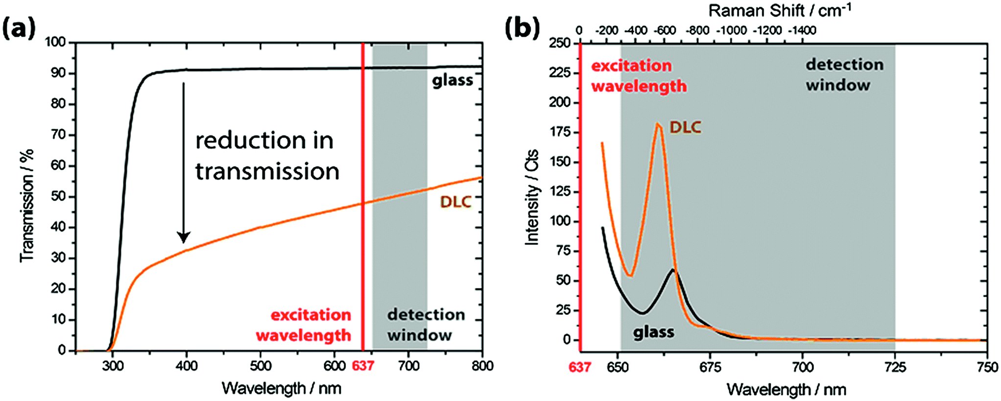 | ||
| Fig. 3 Transmission (a) and emission (b) spectra of DLC coated glass. The detection window (grey) and excitation wavelength (red) being applied for the TIRF experiments are indicated in the graphs. | ||
In addition to its optical activity, the DLC coating will act as a spacer in TIRF imaging. TIRF imaging relies on the evanescent, near-field wave that is generated at the glass interface. Since the evanescent field decays exponentially from the interface (in about 100–200 nm), the DLC coating effectively reduces the excitation of fluorophores sitting on top of it. Based on these observations, we expect the imaging signal for patterns prepared with MACE-ID to be limited when combined with a DLC coating.
Fig. 4a shows the results of the functionalization using an adaption of the MACE-ID strategy, i.e. the labeling of electron beam written nanostructures on a coating (Fig. 1b, option II). SiOx squares deposited on top of the diamond-like carbon (DLC) are faintly visible in the SEM image, as the contrast between the DLC and SiOx thin film is low. The sample is silanized with 3-aminopropyl-dimethyl-ethoxysilane (APDMES) and labeled with the fluorophore ATTO655-NHS. When imaged in TIRF mode, the contrast is high. The background intensities in the image are low, while the SiOx deposits are clearly visible.
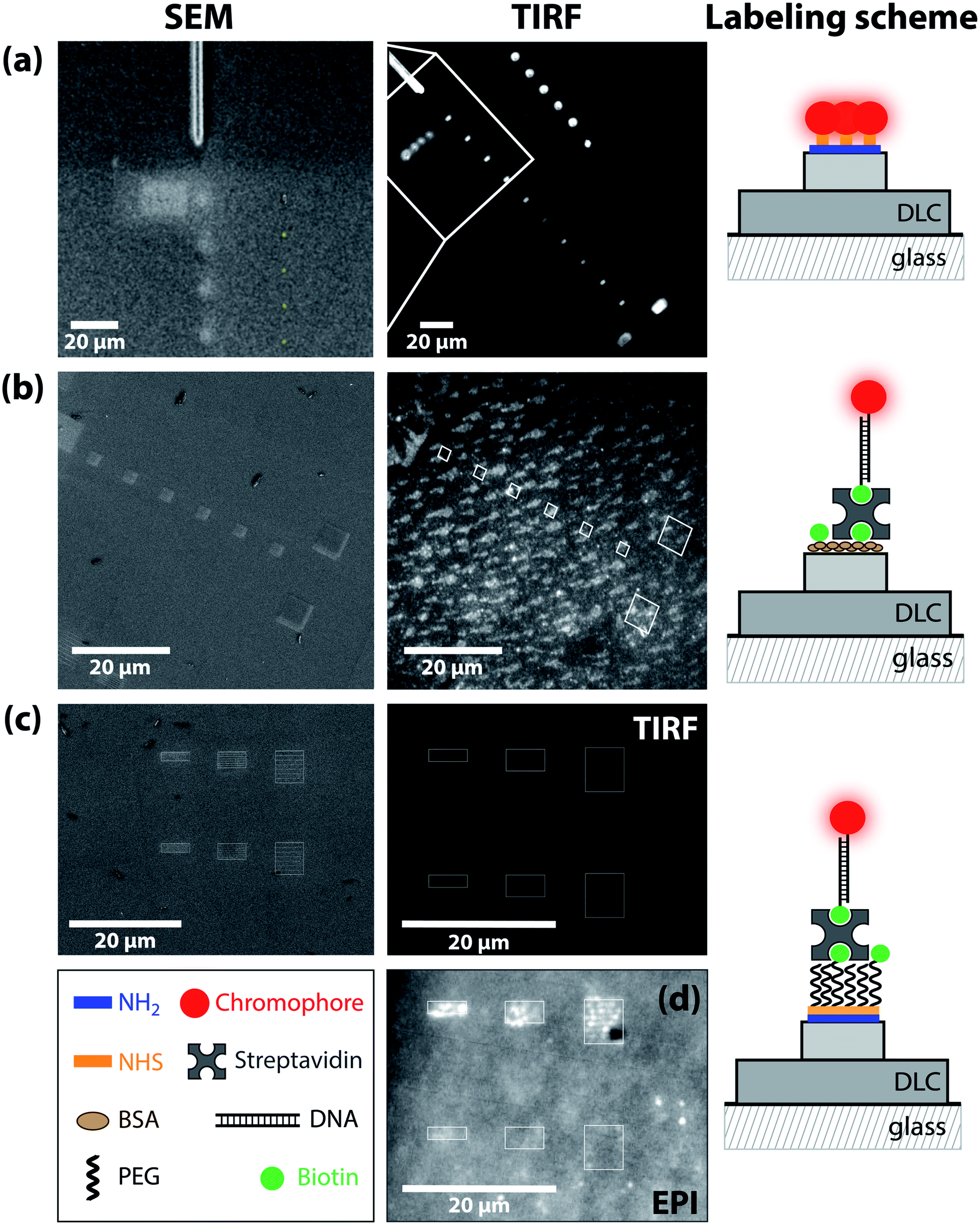 | ||
| Fig. 4 FEB SiOx structures characterized by SEM and TIRF imaging. (a) The activated surface is labeled directly with ATTO655-NHS. (b) The SiOx is passivated with biotin/BSA and labeled with ATTO655-linked, biotinylated DNA. (c) The SiOx is passivated with biotin/PEG via neutravidin and labeled with ATTO655-linked, biotinylated DNA. The pattern is only weakly visible in TIRF. (d) The same pattern from (c) is visible in epi-fluorescence. | ||
We observe in our experiments that, when patterned glass is silanized and functionalized directly, nonspecific binding occurs. On the locally exposed surface there are not only fluorophores covalently bound to the silanes (as intended), but also fluorophores that stay on the glass surface through physisorption or chemisorption. To prevent unspecific and noncovalent binding of fluorophores to the surface, we first passivated the SiOx deposits with BSA (Fig. 4b). Fig. 4b shows a passivated sample with BSA/BSA-biotin and subsequent labeling with ATTO655-linked dsDNA oligomers, immobilized via neutravidin–biotin interactions. The SEM image shows the SiOx squares written with the electron beam, but TIRF microscopy reveals a significant background signal and a poor signal from the labeled structures. In addition, fluorescent islands are visible outside the patterned area, suggesting that aggregates of the BSA/DNA-fluorophore are present on DLC.
Fig. 4c shows the results of the second approach, in which we passivate the SiOx deposits with PEG/PEG-biotin and label them with ATTO655-linked dsDNA via neutravidin–biotin interaction. The SEM image shows two groups of deposited SiOx lines written by MACE-ID with 4000 and 8000 scans each. The 50 nm wide lines are spaced at 800, 400 and 250 nm. TIRF microscopy shows no fluorescent background around the written patterns, but also shows no detectable signal of the labeled deposits themselves. To verify that the SiOx are labeled, the written glass slide is inverted and inspected in epi-fluorescent mode. Although the signal-to-noise ratio is poor (due to the buffer layer used in epi-fluorescence mode), Fig. 4d indeed shows that the SiOx patterns are labeled via biotin–neutravidin in combination with PEG as the passivation layer.
The results show that the BSA passivation layer physisorbs to the surface and does not selectively bind to the SiOx deposits. And while the PEG/PEG-biotin is bound covalently to the activated surface and allows controlled and selective labeling, from Fig. 4c it is clear that the SiOx deposits are not observed in TIRF. From these results we conclude that it is caused by the DLC coating and the PEG/PEG-biotin; together they place the fluorophore relatively far from the glass interface and outside the evanescent field of excitation. This explains the absence of fluorescence intensity in Fig. 4c. In addition to this, the DLC coating attenuates the fluorescence signal of any labeled structure that sits on top of the coating due to its optical properties (as shown in Fig. 3).
To exploit the optical properties of the DLC coating (rather than to be limited by it) we locally remove the DLC using a focused ion beam (Fig. 1b, option I). If a pattern is defined in the DLC layer, the DLC layer itself helps to reduce the background signal of unspecifically bound fluorophores. Based on the data in Fig. 3a we conclude that the coating reduces the background signal significantly compared to the signal of actively etched patterns on glass. Fig. 5 shows the etched depth of 10 by 10 μm2 squares as a function of the number of scans at a beam current of 10 nA. The thickness of the DLC coating is estimated from the SEM images; when the glass surface is exposed the contrast reverses due to charging. In Fig. 5a it is observed that this happens at 150 scans. A characterization using AFM reveals the depth profile within the structure as a function of the sputtering dosis (Fig. 5b). For a small amount of scans there is some deposition, rather than etching. We speculate that this is due to a local roughening of the surface, combined with deposition due to minor contamination in the vacuum system. However, etching is observed with proceeding scans (etch rate is about −0.8 +/− 0.02 nm/scan). This data shows that 150 scans are sufficient to fully etch through the ∼60 nm DLC layer and expose the glass.
 | ||
| Fig. 5 The etched depth as function of the number of scans. (a) SEM image showing a series of 10 by 10 μm squares with increasing amount of scans. From the contrast reversal it is concluded that the DLC coating is fully removed at 150 scans. (b) Depth profile of the corresponding, etched terraces measured using the AFM. The DLC layer (depicted in grey) is about 60 nm thick. From about 50 scans onwards DLC is removed from the glass and shows a linear sputtering rate of about −0.8 +/− 0.02 nm/scan. | ||
Fig. 6 shows patterns etched into the DLC coating using the focused ion beam etching of the DLC coating, imaged using the SEM and (after functionalization) TIRF microscopy. We show functionalization without (Fig. 6a) and with glass passivation (Fig. 6b–d). The SEM images (Fig. 6a) reveal regularly spaced lines and crosses. Investigating the sample with TIRF microscopy after labeling with ATTO655, it is observed that only the crosses are bright, while the lines remain dark. This is because the lines are not etched through the coating and the underlying glass is not exposed. Comparing the intensities of the functionalized crosses and the DLC background, we observe high contrast and a low fluorescent background. In Fig. 6b, BSA/BSA-biotin is used to passivate the exposed glass surface and the lines are labeled with ATTO655-linked dsDNA oligomers, which are immobilized via neutravidin–biotin interactions. The SEM image shows a series of lines of 400 nm wide and around 7.5 μm long. Although TIRF microscopy reveals that the pattern is labeled with fluorophores, other features are visible in the background as well. These features are most likely BSA-aggregates on the DLC coating, as have been observed also for the MACE-ID structures in Fig. 4b.
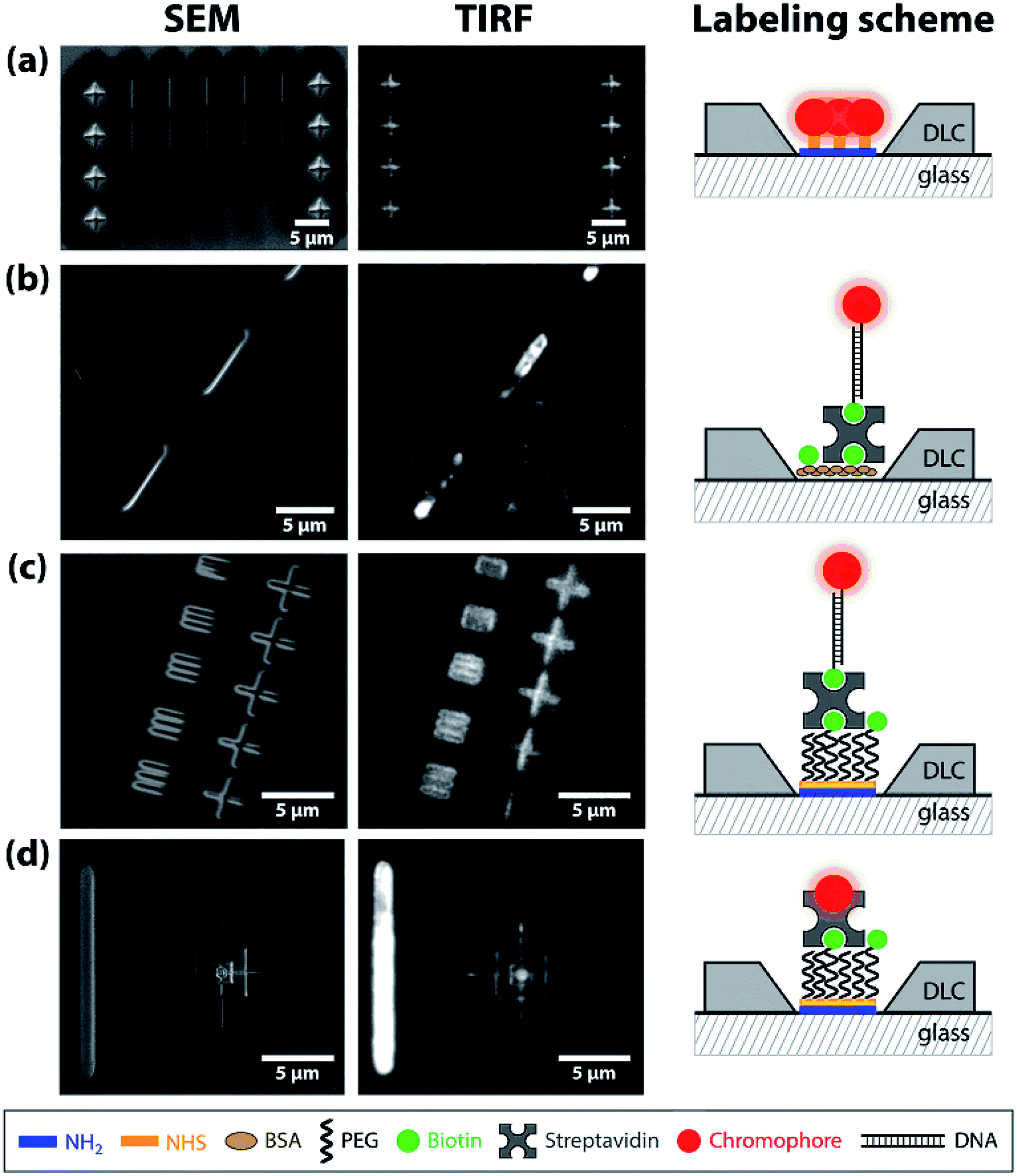 | ||
| Fig. 6 Patterns etched with the focused ion beam, characterized using SEM and TIRF imaging. Activated surfaces were labeled (a) directly with ATTO655-NHS or (b–d) with a passivation layer in between. Making use of biotin–neutravidin interactions, the patterns were labeled with (b) ATTO655-biotinylated DNA on the BSA- or (c) PEG-surface, respectively. (d) Cy5 is bound to streptavidin, with a ratio of 4:3 for PEG/PEG-biotin, respectively. | ||
When the pattern is passivated and silanized with PEG/PEG-biotin (Fig. 6c and d), the passivation layer is specifically bound to the silanized patterns by NH2–NHS-binding and unselective functionalization is not observed. When the PEG/PEG-biotin is labeled with DNA-ATTO655 (Fig. 6c) or streptavidin-Cy5 (Fig. 6d) the pattern is clearly visible. An improved signal-to-noise ratio can be achieved for streptavidin-Cy5, since it is easily excited on the TIRF microscope due to its height above the glass surface.
To verify that the biotin–streptavidin interaction is selective and specific, we expose a silanized PEG-surface to biotinylated DNA. Fig. 7a shows a bright field image of DLC coated glass with FIB-etched lines. Fluorescence is not observed if there is only biotinylated ATTO655-DNA (Fig. 7b) or neutravidin (Fig. 7c) on the surface. Only after incubation with neutravidin binding of biotinylated DNA to the surface is observed, seen by the intensity increase over time (Fig. 7d–e). The underlying kinetics follows a simple binding as described for a biotin–avidin interaction.37 This demonstrates that the nanostructures are selectively labeled.
 | ||
| Fig. 7 Specific labeling by ATTO655-labeled DNA via biotin–neutravidin interaction on a FIB patterned glass coated with PEG/PEG-biotin. (a) Bright field image. TIRF image of the same surface exposed to (b) 2 nM ATTO655-labeled DNA, (c) 0.2 mg ml−1 neutravidin and (d) 2 nM ATTO655-labeled DNA after incubation with neutravidin. Biotinylated DNA binds exclusively after addition of neutravidin to the surface. (e) The intensity averaged over 512 × 512 pixels as a function of time, showing the increasing labeling with incubation time. | ||
4. Conclusion
We present a novel approach to combine the bottom-up assembly and high-resolution lithography to position functional molecules on glass. The glass is coated with a 60 nm thick diamond-like carbon film. A pattern is defined by either writing SiOx on the film with a focused electron beam, or exposing the underlying glass by focused ion beam etching. The patterns are silanized and labeled with a variety of functional groups, such as (but not limited to) ATTO655 and Cy5. The approach enables imaging of the patterns with TIRF microscopy. We demonstrate that the labeling is selective and that the patterns can be imaged with high signal-to-noise ratios.The approach enables us to both position functional groups on a surface and to verify their positions and surface concentrations accurately. Our approach promises to benefit, amongst others, single-molecule biophysics studies and studies using zero-mode waveguides.38,39 The specific positioning of single fluorescently labeled molecules, such as DNA, proteins, or viruses simplifies data analysis and provides a solution for the problem of unspecific binding in single-molecule experiments.
Acknowledgements
E. P. acknowledges a DFG fellowship (PL696/2-1). B.L.F. was supported by the Ministry for Science and Education (Gravity program). W.F.v.D. was supported by a Veni grant (Grant no. 10684 – STW-Utrecht) and the Zernike Institute for Advanced Materials. T. C. was supported by the Zernike Institute for Advanced Materials and the Centre for Synthetic Biology (University of Groningen). We are grateful to A. M. van Oijen and B. Poolman for support and access to laboratory facilities. We finally thank M. Punter and V. Krasnikov for help with data analysis and experiments.References
- A. Chan, R. P. Orme, R. A. Fricker and P. Roach, Adv. Drug Delivery Rev., 2013, 65, 497–514 CrossRef CAS PubMed.
- H. E. Huxley, Science, 1969, 164, 1356–1366 CAS.
- Y. Salomon, M. Lin, C. Londos, M. Rendell and M. Rodbell, J. Biol. Chem., 1975, 250, 4239–4245 CAS.
- M. Lin, Y. Salomon, M. Rendell and M. Rodbell, J. Biol. Chem., 1975, 250, 4246–4252 CAS.
- M. Rendell, Y. Salomon, M. Lin, M. Rodbell and M. Berman, J. Biol. Chem., 1975, 250, 4253–4260 CAS.
- D. A. Leigh, J. K. Wong, F. o. Dehez and F. Zerbetto, Nature, 2003, 424, 174–179 CrossRef CAS PubMed.
- R. Eelkema, M. M. Pollard, J. Vicario, N. Katsonis, B. S. Ramon, C. W. Bastiaansen, D. J. Broer and B. L. Feringa, Nature, 2006, 440, 163–163 CrossRef CAS PubMed.
- B. Lewandowski, G. De Bo, J. W. Ward, M. Papmeyer, S. Kuschel, M. J. Aldegunde, P. M. Gramlich, D. Heckmann, S. M. Goldup and D. M. D'Souza, Science, 2013, 339, 189–193 CrossRef CAS PubMed.
- S. J. van der Molen, J. Liao, T. Kudernac, J. S. Agustsson, L. Bernard, M. Calame, B. J. van Wees, B. L. Feringa and C. Schönenberger, Nano Lett., 2008, 9, 76–80 CrossRef PubMed.
- C. Raimondo, N. Crivillers, F. Reinders, F. Sander, M. Mayor and P. Samori, Proc. Natl. Acad. Sci. U. S. A., 2012, 109, 12375–12380 CrossRef CAS PubMed.
- B. K. Pathem, S. A. Claridge, Y. B. Zheng and P. S. Weiss, Annu. Rev. Phys. Chem., 2013, 64, 605–630 CrossRef CAS PubMed.
- G. London, K.-Y. Chen, G. T. Carroll and B. L. Feringa, Chem. – Eur. J., 2013, 19, 10690–10697 CrossRef CAS PubMed.
- D. Janssen, R. De Palma, S. Verlaak, P. Heremans and W. Dehaen, Thin Solid Films, 2006, 515, 1433–1438 CrossRef CAS PubMed.
- T. Kudernac, N. Katsonis, W. R. Browne and B. L. Feringa, J. Mater. Chem., 2009, 19, 7168–7177 RSC.
- C. J. Barrett, J.-i. Mamiya, K. G. Yager and T. Ikeda, Soft Matter, 2007, 3, 1249–1261 RSC.
- V. Balzani, A. Credi and M. Venturi, ChemPhysChem, 2008, 9, 202–220 CrossRef CAS PubMed.
- A. G. Curto, G. Volpe, T. H. Taminiau, M. P. Kreuzer, R. Quidant and N. F. van Hulst, Science, 2010, 329, 930–933 CrossRef CAS PubMed.
- O. Arcizet, V. Jacques, A. Siria, P. Poncharal, P. Vincent and S. Seidelin, Nat. Phys., 2011, 7, 879–883 CrossRef CAS.
- V. Auzelyte, C. Dais, P. Farquet, D. Grützmacher, L. J. Heyderman, F. Luo, S. Olliges, C. Padeste, P. K. Sahoo and T. Thomson, J. Micro/Nanolithogr., MEMS, MOEMS, 2009, 8, 021204–021210 CrossRef PubMed.
- V. R. Manfrinato, L. Zhang, D. Su, H. Duan, R. G. Hobbs, E. A. Stach and K. K. Berggren, Nano Lett., 2013, 13, 1555–1558 CAS.
- W. F. Van Dorp, X. Zhang, B. L. Feringa, T. W. Hansen, J. B. Wagner and J. T. M. De Hosson, ACS Nano, 2012, 6, 10076–10081 CrossRef CAS PubMed.
- C. M. Kolodziej and H. D. Maynard, Chem. Mater., 2012, 24, 774–780 CrossRef CAS.
- T. Baumgärtel, C. von Borczyskowski, H. Graaf and Beilstein, J. Nanotechnol., 2013, 4, 218–226 Search PubMed.
- L. Demers, D. Ginger, S.-J. Park, Z. Li, S.-W. Chung and C. Mirkin, Science, 2002, 296, 1836–1838 CrossRef CAS PubMed.
- K. Salaita, Y. Wang, J. Fragala, R. A. Vega, C. Liu and C. A. Mirkin, Angew. Chem., 2006, 118, 7378–7381 CrossRef.
- S. K. Kufer, E. M. Puchner, H. Gumpp, T. Liedl and H. E. Gaub, Science, 2008, 319, 594–596 CrossRef CAS PubMed.
- W. Slingenbergh, S. K. de Boer, T. Cordes, W. R. Browne, B. L. Feringa, J. P. Hoogenboom, J. T. M. De Hosson and W. F. van Dorp, ACS Nano, 2012, 6, 9214–9220 CrossRef CAS PubMed.
- T. Ha and P. Tinnefeld, Annu. Rev. Phys. Chem., 2012, 63, 595–617 CrossRef CAS PubMed.
- E. Betzig, G. H. Patterson, R. Sougrat, O. W. Lindwasser, S. Olenych, J. S. Bonifacino, M. W. Davidson, J. Lippincott-Schwartz and H. F. Hess, Science, 2006, 313, 1642–1645 CrossRef CAS PubMed.
- S. T. Hess, T. P. Girirajan and M. D. Mason, Biophys. J., 2006, 91, 4258–4272 CrossRef CAS PubMed.
- M. J. Rust, M. Bates and X. Zhuang, Nat. Methods, 2006, 3, 793–795 CrossRef CAS PubMed.
- T. Cordes, M. Strackharn, S. W. Stahl, W. Summerer, C. Steinhauer, C. Forthmann, E. M. Puchner, J. Vogelsang, H. E. Gaub and P. Tinnefeld, Nano Lett., 2010, 10, 645–651 CrossRef CAS PubMed.
- J. Vogelsang, T. Cordes, C. Forthmann, C. Steinhauer and P. Tinnefeld, Proc. Natl. Acad. Sci. U. S. A., 2009, 106, 8107–8112 CrossRef CAS PubMed.
- R. Roy, S. Hohng and T. Ha, Nat. Methods, 2008, 5, 507–516 CrossRef CAS PubMed.
- Y. Sako, Imaging single molecules in living cells for systems biology, Mol. Syst. Biol., 2006, 2 DOI:10.1038/msb4100100.
- T. Sameshima and N. Andoh, Jpn. J. Appl. Phys., 2005, 44, 7305–7308 CrossRef CAS.
- J. R. Wayment and J. M. Harris, Anal. Chem., 2009, 81, 336–342 CrossRef CAS PubMed.
- P. Hinterdorfer and A. Van Oijen, Handbook of single-molecule biophysics, Springer, 2009 Search PubMed.
- P. Zhu and H. G. Craighead, Annu. Rev. Biophys., 2012, 41, 269–293 CrossRef CAS PubMed.
| This journal is © The Royal Society of Chemistry 2014 |