
 Open Access Article
 This Open Access Article is licensed under a Creative Commons Attribution-Non Commercial 3.0 Unported Licence
Air-processed inverted organic solar cells utilizing a 2-aminoethanol-stabilized ZnO nanoparticle electron transport layer that requires no thermal annealing†
Il
Jeon
a,
James W.
Ryan
a,
Tafu
Nakazaki
b,
Kee Sheng
Yeo
a,
Yuichi
Negishi
b and
Yutaka
Matsuo
*a
aDepartment of Chemistry, School of Science, The University of Tokyo, 7-3-1 Hongo, Bunkyo-ku, Tokyo 113-0033, Japan. E-mail: matsuo@chem.s.u-tokyo.ac.jp
bDepartment of Applied Chemistry, Tokyo University of Science, 1-3 Kagurazaka, Shinjuku, Tokyo 162-8601, Japan
First published on 12th September 2014
Abstract
Highly stable ZnO nanoparticles (NPs) for use in organic solar cells (OSCs) have been synthesized in 2-aminoethanol, which acts as both a stabilizing ligand and a solvent. The ZnO NP films do not require thermal annealing and applying them in inverted P3HT:mix-PCBM OSCs fabricated almost entirely under ambient conditions show efficiencies >3%. We find that thermally annealing the ZnO NP films does not give rise to any significant differences in device performance up to 150 °C. Annealing the films at higher temperatures leads to reduced short-circuit current densities and fill factors due to the removal of 2-aminoethanol from the NP surface, as evidenced by X-ray photoelectron spectroscopy. Furthermore, to confirm that the post-annealing of P3HT:PCBM devices at 150 °C does not affect our results, we fabricated inverted small molecule OSCs using a squaraine donor and PC71BM acceptor that only requires a low-temperature thermal annealing step (70 °C). No substantial differences between annealed and non-annealed devices were observed, which demonstrates the applicability of these new ZnO NPs in flexible OSCs.
Introduction
Organic solar cells (OSCs) have demonstrated their potential as next-generation light harvesting devices for supplying a significant quota of the world's energy in a clean and efficient manner.1 In the past number of years significant advances have been made that have lead to OSC efficiencies reaching 10%.2 As efficiencies continue to increase so does the need for industrial considerations to be addressed, such as improving device stability and lowering fabrication costs.3 In a normal architecture OSC, the device relies on the use of a low work function top electrode that is highly susceptible to degradation from oxygen and water, as are many of the organic materials that make up the active and interfacial layers. The final steps of device fabrication must therefore be carried out under dry anaerobic conditions and, prior to exposing the device to ambient conditions, a potentially costly encapsulation layer must be incorporated. Inverting the architecture, however, allows the use of high work function electrodes such as silver and gold, as well as air-stable metal oxide transport layers, which provide added protection to the active layer.4 MoO3 is typically employed as the hole transport layer (HTL) for reducing Ohmic losses between the donor's HOMO and the Au or Ag anode.4a,5 PEDOT:PSS can also be utilized as the HTL, having the advantage of being easily deposited via spin-coating on top of the active layer.6 The most common electron-transport materials are ZnO and TiO2, which offer high electron transport between the fullerene and the ITO interface.7 However one common drawback does exist with these materials, which is that a high temperature step is required. For most deposition methods of ZnO and TiO2 films annealing temperatures in excess of 150 °C are generally required,4b,7a which is well above the glass transition temperature of common polymeric substrates used in flexible organic electronic devices. During the preparation of this manuscript, Lu and Tao et al. reported a method for depositing ZnO films that does not require thermal annealing, using an air-sensitive ZnO NP solution.8 Here, we demonstrate a new and facile synthesis route for obtaining highly stable ZnO nanoparticle (NP) solutions for fabricating low-temperature ZnO films that can be applied as ETLs in OSCs. The NPs are synthesized in 2-aminoethanol and do not require any additional stabilizers or ligands, aside from the solvent molecules themselves. Furthermore, the ZnO films can be readily processed in air. Inverted OSCs were fabricated with the ZnO NP films subjected to various annealing temperatures, where the active layer was P3HT:mix-PCBM, mix-PCBM corresponds to a mixture of PC61BM (85 wt%) and PC71BM (15 wt%) that is more economical and has been shown to offer higher stability and slightly higher performance than pure PC61BM.9 X-ray photoelectron spectroscopy and atomic force microscopy are employed to study the surface chemistry and topography, respectively. Inverted small molecular OSCs (SMOSCs) using the ZnO NP films are also investigated, based on a squaraine (SQ) donor and a PC71BM acceptor, to demonstrate the potential of this approach for fabricating low-temperature OSCs compatible with flexible substrates.7dResults and discussion
The synthesis of the ZnO NPs is similar to the method used by Lin et al.,10 where we replaced diethylene glycol with a shorter alkyl chained amino alcohol, 2-aminoethanol. The use of 2-aminoethanol allowed a more concentrated solution to be obtained compared with the previous method. The synthesis and isolation of the ZnO NPs is shown in Scheme 1, which consisted of heating zinc acetate (ZnOAc)2 in 2-aminoethanol to 160 °C and refluxing for an hour.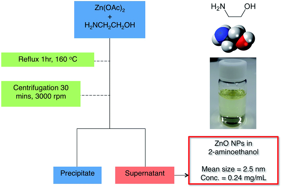 | ||
| Scheme 1 Synthesis and separation of ZnO nanoparticles. | ||
Once the solution was cooled down, it was centrifuged, which led to a precipitate that contained ZnO NPs with diameters in excess of 100 nm and a pale yellow supernatant that provided well dispersed ZnO NPs with a mean diameter of 2.5 nm as determined by transmission electron microscopy (see ESI Fig. S1-1†). The concentration of the solution obtained was 0.24 mg ml−1 and stable for at least 6 months, which, considering that no additional stabilizing ligands were required in addition to the 2-aminoethanol solvent molecules, is an interesting and important finding.
The as-obtained supernatant solution was then used in fabricating OSCs by spin-coating it on indium tin oxide (ITO) patterned glass substrates. Following spin-coating, the films were then subjected to thermal annealing at temperatures ranging from room temperature (i.e. no annealing) to 210 °C. The annealing time was fixed at 1 h in each case. The transmittance of the ZnO thin films on glass/ITO substrates are shown in Fig. 1 and shows a decrease in transmittance with annealing temperature. Non-annealed ZnO NP films show the highest transmittance, with a maximum transmittance of 85.2% at 520 nm.
 | ||
| Fig. 1 Transmittance spectra of ZnO NP films on glass/ITO substrates annealed at different temperatures. | ||
P3HT:mix-PCBM active layers were then deposited, followed by a PEDOT:PSS hole transport layer and Au electrode. Note that all layers, except for gold, were deposited in air. Furthermore, devices were also annealed and measured in air, without the addition of an encapsulation layer, demonstrating the good stability of these inverted devices. The current–voltage (J–V) curves of the OSCs are shown in Fig. 2 and Table 1 summarizes the key figures of merit. Remarkably, devices processed without subjecting the ZnO layer to any thermal annealing have the highest power conversion efficiency (PCE, η) of 3.1% due to the higher fill factor (FF) compared with the annealed devices. Although, the difference between the devices with non-annealed ZnO films and the devices annealed up to 120 °C do not in fact differ considerably. There is, however, a significant difference in η when the annealing temperature exceeds 120 °C, where the FF decreases with increasing temperature as does the short-circuit current density (JSC), with a significant drop observed when annealing exceeds 150 °C. This decrease in FF arises from an increase in series resistance (RS) as well as the shunt resistance (RSh), with values decreasing with annealing temperature (see Table 1). S-shaped curves are observed for devices employing ZnO films annealed at 210 °C, which further decreases the FF. The origin of the S-shaped kink in the J–V curve is not entirely clear but probably arises from ZnO inducing a barrier to charge injection or extraction.11 Considering that 2-aminoethanol should have been removed from the ZnO NP surface due to the high annealing temperature (at least for the NPs on the ZnO surface), we would expect the NPs to have a high concentration of trap states that may reduce the conductivity of the ZnO film as well as act as trap-sites for free charge carriers generated in the active layer. All devices displayed a short UV-activation time, i.e. light soaking, but there was no noticeable trend between the activation time and the annealing conditions. Reference P3HT:mix-PCBM inverted devices were also fabricated for comparison using a standard sol–gel method to deposit the ZnO film (thermally annealed at 200 °C),4b which shows slightly higher but not significantly different performance (η = 3.2%), demonstrating the high applicability of our ZnO NP approach in OSCs. We have fabricated devices using ZnO NPs synthesized in ethylene glycol and found that they do not perform as well as ZnO NPs in 2-aminoethanol. (see ESI Fig. S3†) We attribute this to the larger diameter of the ZnO NPs (4.09 nm on average) that also display a larger size deviation than the ZnO NP in 2-aminoethanol (see also ESI Fig. S1-2†).
 | ||
| Fig. 2 J–V curves for inverted P3HT:mix-PCBM devices where the ZnO NP film was subject to various annealing temperatures measured under (a) 1 Sun illumination (AM 1.5 G, 100 mW cm−2) and (b) dark conditions. Non-annealed (black), 120 °C (blue), 150 °C (purple), 180 °C (red) and 210 °C (green). | ||
| Annealing temperature | V OC V | J SC mA cm−2 | FF | η% | R S Ω cm2 | R Sh Ω cm2 |
|---|---|---|---|---|---|---|
| a Sol–gel reference devices. | ||||||
| NA | 0.61 | 9.08 | 0.56 | 3.1 | 8.29 | 1660 |
| 120 °C | 0.62 | 9.13 | 0.53 | 3.0 | 8.43 | 1540 |
| 150 °C | 0.62 | 8.65 | 0.53 | 2.9 | 8.35 | 1270 |
| 180 °C | 0.61 | 7.98 | 0.45 | 2.2 | 9.77 | 1220 |
| 210 °C | 0.59 | 6.91 | 0.34 | 1.4 | 20.11 | 1120 |
| 200 °Ca | 0.60 | 9.42 | 0.56 | 3.2 | 5.71 | 2230 |
Investigating the effect of thermal annealing on the thin film properties of ZnO, we found that the topography, as measured by atomic force microscopy (AFM) on ITO/Glass substrates, did not change significantly with rms roughness values between 5 and 6 nm (Fig. 3). Non-annealed films had the roughest topography and it can be seen that upon annealing at 120 °C, the roughness decreases and then increases with temperature. The changes are subtle, however, and are probably not significant enough to explain the large changes in the J–V characteristics.
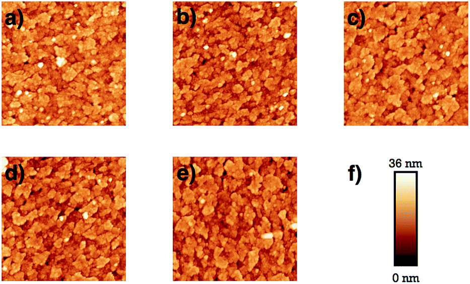 | ||
| Fig. 3 Atomic force microscopy topography images of ZnO NP thin films corresponding to the following annealing conditions: (a) non-annealed, (b) 120 °C, (c) 150 °C, (d) 180 °C and (e) 210 °C. The area scanned for each image was 5 × 5 μm and (f) the Z-scale for each image is also identical. | ||
The surface chemistry of the ZnO films was then probed using X-ray photoelectron spectroscopy (XPS). Fig. 4 shows the peaks of ZnO films corresponding to (a) Zn 2p3/2 and (b) N 1s core levels (refer to the ESI† for the wide-scan images of each film). A positive shift in the binding energy (BE) of ∼1 eV is observed for both Zn 2p3/2 and N 1s peaks when the films are annealed at 150 °C and above. This increase in BE for both Zn and N indicates that 2-aminoethanol is cleaved from the surface of the ZnO NPs. Furthermore, the intensity of the 2-aminoethanol peaks is seen to decrease with annealing temperature, even for the films annealed at 120 °C, which is much lower than the boiling point of 2-aminoethanol (170 °C). The ∼1 eV increase in BE for both Zn and N does not exactly reflect the trend observed in the J–V curves above, as the device employing a ZnO film annealed at 150 °C still has relatively high efficiency even though 2-aminoethanol has been cleaved from the ZnO surface. However, when the films are annealed at temperatures above the boiling point of 2-aminoethanol we do see a significant decrease in the performance. These results suggest that the presence of 2-aminoethanol is important. Indeed, a recent study on a polar solvent treatment of rippled-ZnO films by Song and co-workers has shown that treating the metal oxide film with a solution of 2-methoxyethanol and just 1% 2-aminoethanol enhances the electrical contact between the ZnO and the LUMO of PCBM.12
 | ||
| Fig. 4 X-ray photoelectron spectroscopy spectra of ZnO films corresponding to (a) N 1s and (b) Zn 2p3/2 under the following annealing conditions: non-annealed (black), 120 °C (blue), 150 °C (purple), 180 °C (red) and 210 °C (green). | ||
The spectra for the O 1s core level are shown in Fig. 5, which correspond to the O in ZnO. We observe an asymmetric peak for each sample that was deconvoluted using curve-fitting methods into two peaks centered at 529.7 ± 0.5 eV (O1) and 531.1 ± 0.5 eV (O2) that correspond to O2− ions of the Zn–O bond for the ZnO wurtzite structure and oxygen deficient component of ZnO where O2− ions correspond to the hydroxyl groups, respectively.13 The ratio of O1![[thin space (1/6-em)]](https://www.rsc.org/images/entities/char_2009.gif) :O2 is seen to change with annealing temperature. O1 is slightly more dominant in the non-annealed ZnO film (O1:O2 = 55:45). Upon annealing at 120 °C in air, O2 is the slightly more dominant species (48:52). However, the percentage of O2 recorded for films heated at higher temperatures proceeds to decrease with temperature. For films annealed at 210 °C the O1:O2 ratio is 60:40. It is difficult to correlate these data with the experimental J–V curves, as one would expect a decrease of hydroxyl groups to correlate with a decrease in the number of trap states and thus better performance, particularly concerning the FF. The opposite trend until 120 °C is observed, however, due to the removal of 2-aminoethanol. It could be possible that the OH group of 2-aminoethanol is also partially responsible for the peaks centered at 531 eV.
:O2 is seen to change with annealing temperature. O1 is slightly more dominant in the non-annealed ZnO film (O1:O2 = 55:45). Upon annealing at 120 °C in air, O2 is the slightly more dominant species (48:52). However, the percentage of O2 recorded for films heated at higher temperatures proceeds to decrease with temperature. For films annealed at 210 °C the O1:O2 ratio is 60:40. It is difficult to correlate these data with the experimental J–V curves, as one would expect a decrease of hydroxyl groups to correlate with a decrease in the number of trap states and thus better performance, particularly concerning the FF. The opposite trend until 120 °C is observed, however, due to the removal of 2-aminoethanol. It could be possible that the OH group of 2-aminoethanol is also partially responsible for the peaks centered at 531 eV.
 | ||
| Fig. 5 XPS spectra of the O 1s peaks of the ZnO films under the following annealing conditions: (a) non-annealed, (b) 120 °C, (c) 150 °C, (d) 180 °C and (e) 210 °C. The orange and blue fits correspond to the deconvoluted O2− species, the former being an oxygen deficient species and the latter peak consistent with that of O2− in a perfect wurtzite crystal. The raw data are represented by red circles along with best fits shown as a black line. | ||
While a clear trend in device performance with ZnO annealing temperature is observed, it must be remembered that the device undergoes a post-annealing process at 150 °C to improve the active layer morphology, which may anneal ZnO in the process and affect the surface chemistry of the ZnO NPs. Therefore, to minimize the influence of the device annealing temperature, we fabricated inverted small molecule organic solar cells (SMOSCs) that only require the active layer to be annealed at 70 °C based on a squaraine donor, 2,4-bis[4-(N,N-diisobutylamino)-2,6-dihydroxyphenyl] squaraine (SQ)14 and a PC71BM acceptor.15 Active layers were prepared by spin-coating a 20 mg ml−1 solution of SQ:PC71BM in chloroform; the donor:acceptor ratio was 1:5 (see the Experimental section for a detailed description of device fabrication). Fig. 6 shows the J–V curves recorded under standard 1 Sun illumination conditions for devices using non-annealed ZnO NP films as well as films annealed at 120 °C and 150 °C. We observed very little difference between the device characteristics, with PCEs of approximately 3% (see Table 2). While the FF for each device is low, it does not differ significantly to what is reported for normal-architecture SQ:PC71BM devices, which generally have FFs between 40 and 45%.15,16 We expect that through optimizing device fabrication, higher PCE can be achieved. However, the main focus here is simply to demonstrate that the ZnO NP films do not require high temperature thermal annealing for efficient OSCs, which is clearly evident in the J–V curves in Fig. 6.
 | ||
| Fig. 6 J–V curves under 1 Sun illumination (AM 1.5 G, 100 mW cm−2) for inverted SQ:PC71BM devices where the ZnO NP film was annealed at 120 °C (blue, triangles) and 150 °C (black, circles) as well as non-annealed (pink, squares). | ||
| Annealing temperature | V OC V | J SC mA cm−2 | FF | η% |
|---|---|---|---|---|
| NA | 0.84 | 9.74 | 0.36 | 3.0 |
| 120 °C | 0.82 | 10.41 | 0.36 | 3.0 |
| 150 °C | 0.82 | 9.96 | 0.38 | 3.1 |
Conclusions
We have demonstrated a new route for the synthesis of highly stable and high performance ZnO films for inverted OSCs that requires no thermal annealing. Applying thermal annealing post-deposition was found to severely affect device performance for temperatures above 150 °C, due to the desorption of 2-aminoethanol from the ZnO NP surface, as evidenced by XPS. Inverted P3HT:mix-PCBM devices employing the ZnO NP films showed respectable efficiencies of ∼3%, which is on par with devices utilizing a conventional ZnO sol–gel derived ETL. As the P3HT:mix-PCBM devices underwent a post-deposition thermal annealing step at 150 °C, we investigated whether this affected the ZnO NP film by fabricating low-temperature SQ:PC71BM devices that only required thermal annealing of 70 °C. For these small molecule OSC devices, no significant differences were observed for devices employing non-annealed ZnO films to those using ZnO films annealed at temperatures up to 150 °C. The long shelf life of the ZnO NP solution coupled with the ability to form high performance ZnO films is an important finding and we hope that this approach will find applications in not only OSCs but also in other organic and organic–inorganic electronic devices.Experimental section
ZnO nanoparticle synthesis
For the chemical synthesis of ZnO nanoparticles (NPs) in 2-aminoethanol the following commercially available chemicals were used without further purification: zinc(II) acetate, Zn(CH3COO)2 (Wako, 99%) and 2-aminoethanol, C2H4(OH)(NH2) (Wako, 99%). The ZnO NPs were synthesized in a similar manner to the methodology reported by Lin et al. but using a lower b.p. solvent, 2-aminoethanol (b.p. 170 °C).10 Firstly, 0.49 mg (0.1 mol) of zinc(II) acetate Zn(CH3COO)2 was added to 2-aminoethanol (100 ml) and heated up to 160 °C in an oil bath and the solution was stirred and refluxed for 1 hour under isothermal treatment. The purpose of reflux was to remove any by-products such as water or acetic acid produced during the reaction. After 1 hour, the resulting solution was cooled to room temperature. The solution was then centrifuged for 30 minutes to remove precipitates. The supernatant contained well-dispersed ZnO nanoparticles with an average size of 2.5 nm, as observed from TEM. This supernatant was collected as the product and was stable for at least 6 months.For the chemical synthesis of ZnO nanoparticles NPs in ethylene glycol, zinc(II) acetate, Zn(CH3COO)2 (Wako, 99%) and ethylene glycol, C2H4(OH)2 (Wako, 99.0%) were used. The ZnO NPs were synthesized in the same manner as the ZnO NPs in 2-aminoethanol as aforementioned.
Preparation of ZnO sol–gel films
The ZnO sol–gel films were prepared using the method reported by Heeger and co-workers.4b,13b A 0.1 M solution of zinc acetate dihydrate [Zn(CH3COO)·(2H2O] (Wako, 99.0%) in ethanol (Wako, 99.5%) was prepared and then subjected to rigorous stirring for 2–3 h at 80 °C. Next, an ethanolamine stabilizer (28% in weight) was added and the solution was left stirring for a further 12–15 h at 60 °C.Device fabrication
ITO substrates (22 × 38 mm2) with a sheet resistance of 6 Ω per square (Kuramoto Co., Ltd.) were first etched using Zn and 1 M HCl, followed by sonicating the substrates sequentially in cleaning surfactants (Semi Clean, M-Lo), water, acetone and 2-isopropanol for 15 minutes each. The substrates were then dried in an oven at 70 °C. Prior to ZnO deposition, ITO substrates were exposed to UV/O3 for 30 min. ZnO NPs in 2-aminoethanol were then deposited onto ITO substrates through a cellulose acetate filter (0.45 μm pore size) by spin coating at a spin speed of 950 rpm for 30 seconds followed by 5000 rpm for a further 30 seconds to remove the remnant solvent. The thickness of the ZnO film was below the resolution of the surface profilometer and estimated to be less than 20 nm. Next the samples (where applicable) were annealed at temperatures between 120 °C and 210 °C for 1 h. Sol–gel ZnO films were prepared by spin-coating the precursor solution at 3000 rpm for 45 s. The films were then annealed at 200 °C for 1 h.P3HT:mix-PCBM devices were fabricated in the following manner. A poly(3-hexylthiophene) (P3HT, regioregular, Sigma Aldrich Chemical Co., Inc.) and mix-PCBM (Frontier Carbon Co., Nanom spectra E124) solution with a donor:acceptor ratio of 5:3 and a concentration of 40 mg ml−1 was prepared in ortho-dichlorobenzene (anhydrous, 99%, Sigma Aldrich Chemical Co., Inc.). The solution was left stirring for 2 h at 65 °C. The solution was then spin-coated on the ZnO layers at a speed of 850 rpm for 60 s to give films of approximately 300 nm. The films were then immediately placed in a Petri-dish for 40 minutes to allow slow evaporation of the solvent. A poly-(3,4-ethylenedioxythiophene)-polystyrenesulfonic acid (PEDOT:PSS) dispersion in water (Clevios P VP, Heraeus Precious Metals GmbH & Co.) containing 0.5 wt% polyoxyethylene(6) tridecyl ether (Sigma Aldrich Chemical Co., Inc.) was spin-coated on top of the active layer to form the hole transport layer with a 30 nm thickness. An approximately 200 nm thick Au layer was thermally evaporated at a pressure of 3 × 10⁻³ Pa, with the use of a shadow mask, which defined the device active area as 1 cm2. Finally, the devices were heated on a hot plate in air at a temperature of 150 °C for 5 min. All processes, except for Au deposition, were performed in air and the devices were not encapsulated.
SQ:PC71BM devices were fabricated on both ZnO NP and sol–gel films from a 20 mg ml−1 CHCl3 solution, where the SQ:PC71BM weight ratio was 1:5. The solution was spin-coated at 3000 rpm for 60 s inside a N2 filled glovebox and the films were then annealed at 70 °C for 10 min. Following annealing, the films were transferred, without exposure to air, to a vacuum chamber, where MoO3 (8 nm) and Au (100 nm) were deposited by thermal evaporation. Devices were encapsulated before measuring their J–V curves. SQ was purchased from Sigma Aldrich and recrystallized by the slow diffusion of MeOH in a saturated solution of SQ in chloroform, following a previously reported method.14 PC71BM was bought from Solenne and was used as received.
Photovoltaic characterization
Current–voltage (J–V) characteristics were measured using a software-controlled source meter (Keithley 2400) under dark conditions and 1 Sun AM 1.5 G simulated sunlight irradiation (100 mW cm−2) using a solar simulator (EMS-35AAA, Ushio Spax Inc.), which was calibrated using a silicon diode (BS-520BK, Bunkyokeiki).Surface characterization
AFM topography images were recorded using a Bruker Multimode atomic force microscope operating in tapping mode. Silicon AFM probes were used that had a nominal frequency of 70 kHz. XPS measurements were carried out on a JEOL photoelectron spectrophotometer (JPS-9010 MC) using a Mg-Kα X-ray source and was calibrated using the C 1s peak of graphite (284.8 eV) as a reference.Acknowledgements
This work was supported by the Funding Program for Next-Generation World-Leading Researchers (GR-30).Notes and references
- S. B. Darling and F. You, RSC Adv., 2013, 3, 17633–17648 RSC.
- (a) M. A. Green, K. Emery, Y. Hishikawa, W. Warta and E. D. Dunlop, Progress in Photovoltaics: Research and Applications, 2014, 22, 1–9 CrossRef; (b) J. You, L. Dou, K. Yoshimura, T. Kato, K. Ohya, T. Moriarty, K. Emery, C.-C. Chen, J. Gao, G. Li and Y. Yang, Nat. Commun., 2013, 4, 1446 CrossRef PubMed.
- D. M. Tanenbaum, M. Hermenau, E. Voroshazi, M. T. Lloyd, Y. Galagan, B. Zimmermann, M. Hosel, H. F. Dam, M. Jorgensen, S. A. Gevorgyan, S. Kudret, W. Maes, L. Lutsen, D. Vanderzande, U. Wurfel, R. Andriessen, R. Rosch, H. Hoppe, G. Teran-Escobar, M. Lira-Cantu, A. Rivaton, G. Y. Uzunoglu, D. Germack, B. Andreasen, M. V. Madsen, K. Norrman and F. C. Krebs, RSC Adv., 2012, 2, 882–893 RSC.
- (a) Z. He, C. Zhong, S. Su, M. Xu, H. Wu and Y. Cao, Nat. Photonics, 2012, 6, 591–595 Search PubMed; (b) A. K. K. Kyaw, D. H. Wang, V. Gupta, J. Zhang, S. Chand, G. C. Bazan and A. J. Heeger, Adv. Mater., 2013, 25, 2397–2402 CrossRef CAS PubMed.
- T. Matsushima, Y. Kinoshita and H. Murata, Appl. Phys. Lett., 2007, 91, 253504 CrossRef PubMed.
- Y. Matsuo, J. Hatano, T. Kuwabara and K. Takahashi, Appl. Phys. Lett., 2012, 100, 063303 CrossRef PubMed.
- (a) T. Kuwabara, H. Sugiyama, M. Kuzuba, T. Yamaguchi and K. Takahashi, Org. Electron., 2010, 11, 1136–1140 CrossRef CAS PubMed; (b) P. P. Boix, J. Ajuria, I. Etxebarria, R. Pacios, G. Garcia-Belmonte and J. Bisquert, J. Phys. Chem. Lett., 2011, 2, 407–411 CrossRef CAS; (c) M. Bolognesi, A. Sanchez-Diaz, J. Ajuria, R. Pacios and E. Palomares, Phys. Chem. Chem. Phys., 2011, 13, 6105–6109 RSC; (d) T. Kuwabara, T. Nakashima, T. Yamaguchi and K. Takahashi, Org. Electron., 2012, 13, 1136–1140 CrossRef CAS PubMed; (e) M. A. Ibrahem, H.-Y. Wei, M.-H. Tsai, K.-C. Ho, J.-J. Shyue and C. W. Chu, Sol. Energy Mater. Sol. Cells, 2013, 108, 156–163 CrossRef CAS PubMed.
- S. Alem, J. Lu, R. Movileanu, T. Kololuoma, A. Dadvand and Y. Tao, Org. Electron., 2014, 15, 1035–1042 CrossRef CAS PubMed.
- Y. Santo, I. Jeon, K. Sheng Yeo, T. Nakagawa and Y. Matsuo, Appl. Phys. Lett., 2013, 103, 073306 CrossRef PubMed.
- K.-F. Lin, H.-M. Cheng, H.-C. Hsu, L.-J. Lin and W.-F. Hsieh, Chem. Phys. Lett., 2005, 409, 208–211 CrossRef CAS PubMed.
- (a) Y. Ho Huh, B. Park and I. Hwang, J. Appl. Phys., 2014, 115, 124504 CrossRef PubMed; (b) W. Tress, K. Leo and M. Riede, Adv. Funct. Mater., 2011, 21, 2140–2149 CrossRef CAS; (c) A. Wagenpfahl, D. Rauh, M. Binder, C. Deibel and V. Dyakonov, Phys. Rev. B: Condens. Matter Mater. Phys., 2010, 82, 115306 CrossRef.
- B. R. Lee, E. D. Jung, Y. S. Nam, M. Jung, J. S. Park, S. Lee, H. Choi, S.-J. Ko, N. R. Shin, Y.-K. Kim, S. O. Kim, J. Y. Kim, H.-J. Shin, S. Cho and M. H. Song, Adv. Mater., 2014, 26, 494–500 CrossRef CAS PubMed.
- (a) L.-J. Meng, C. P. Moreira de Sá and M. P. dos Santos, Appl. Surf. Sci., 1994, 78, 57–61 CrossRef CAS; (b) Y. Sun, J. H. Seo, C. J. Takacs, J. Seifter and A. J. Heeger, Adv. Mater., 2011, 23, 1679–1683 CrossRef CAS PubMed; (c) X. Q. Wei, B. Y. Man, M. Liu, C. S. Xue, H. Z. Zhuang and C. Yang, Phys. Rev. B: Condens. Matter Mater. Phys., 2007, 388, 145–152 CrossRef CAS PubMed; (d) E. De la Rosa, S. Sepúlveda-Guzman, B. Reeja-Jayan, A. Torres, P. Salas, N. Elizondo and M. J. Yacaman, J. Phys. Chem. C, 2007, 111, 8489–8495 CrossRef CAS.
- M. Tian, M. Furuki, I. Iwasa, Y. Sato, L. S. Pu and S. Tatsuura, J. Phys. Chem. B, 2002, 106, 4370–4376 CrossRef CAS.
- G. D. Wei, S. Y. Wang, K. Renshaw, M. E. Thompson and S. R. Forrest, ACS Nano, 2010, 4, 1927–1934 CrossRef CAS PubMed.
- G. Chen, H. Sasabe, Z. Wang, X. Wang, Z. Hong, J. Kido and Y. Yang, Phys. Chem. Chem. Phys., 2012, 14, 14661–14666 RSC.
Footnote |
| † Electronic supplementary information (ESI) available: TEM images of ZnO NPs, wide-scan XPS spectra for each sample, and device performance of ZnO in ethylene glycol based solar cells. See DOI: 10.1039/c4ta04595e |
| This journal is © The Royal Society of Chemistry 2014 |