
 Open Access Article
 This Open Access Article is licensed under a
 Creative Commons Attribution 3.0 Unported Licence
High performance perovskite solar cells by hybrid chemical vapor deposition†
Matthew R.
Leyden
,
Luis K.
Ono
,
Sonia R.
Raga
,
Yuichi
Kato
,
Shenghao
Wang
and
Yabing
Qi
*
Energy Materials and Surface Sciences Unit, Okinawa Institute of Science and Technology Graduate University, 1919-1 Tancha, Onna-son, Okinawa 904-0495, Japan. E-mail: yabing.qi@oist.jp
First published on 24th September 2014
Abstract
Organometal halide based perovskites are promising materials for solar cell applications and are rapidly developing with current devices reaching ∼19% efficiency. In this work we introduce a new method of perovskite synthesis by hybrid chemical vapor deposition (HCVD), and demonstrate efficiencies as high as 11.8%. These cells were found to be stable with time, and retained almost the same efficiency after approximately 1100 h storage in dry N2 gas. This method is particularly attractive because of its ability to scale up to industrial levels and the ability to precisely control gas flow rate, temperature, and pressure with high reproducibility. This is the first demonstration of a perovskite solar cell using chemical vapor deposition and there is likely still room for significant optimization in efficiency.
Introduction
Organometal halide perovskite based solar cells have been rapidly improving in recent years. In 2009 efficiencies were around 4%,1 but in 5 years time that number has more than quadrupled to ∼19%.2–6 Due to perovskite's broad spectral absorbance, low temperature processing, and low cost of materials it is a promising material for low cost solar cells. To achieve easier fabrication and better reproducibility, we used a two-step method of perovskite synthesis where a layer of metal halide (e.g. PbCl2 and PbI2) is deposited, followed by the addition of an ammonium halide salt (e.g. methyl ammonium iodide, formamidinium bromide). In this method, a solid powder is converted to the gas phase in a dedicated zone of the tube furnace and then deposited onto substrates downstream in another zone of the tube furnace. Because of the use of solid precursors, this method can be viewed as a form of hybrid chemical vapor deposition (HCVD). Two-step processes where methyl ammonium halide is deposited by spin coating or vapor phase can reach efficiency as high as 15%.7–11 Perovskite has been previously synthesized by CVD,12,13 but this work is the first to use CVD to demonstrate any solar cell efficiency. The reported stability of perovskite films can vary significantly. In one case, perovskite is reported to decay substantially to 20% of its original performance over the course of 6 days in a N2 environment,6 and in others it is reported to be stable for 500 h in air without encapsulation.14Perovskite solar cells made by HCVD were shown to be stable up to 1100 h in a N2 environment, which warrants further study of stability under ambient conditions.
Results and discussion
Multi-zone HCVD has independent precise control of pressure, gas flow rate, methyl ammonium iodide (MAI) temperature, and substrate temperature, which helps improve reproducibility and performance. For example, by controlling the pressure (1 Pa to 1 atm), the diffusion rate (Dg ∝ T3/2/P, where Dg is the gas diffusion constant, T is the temperature, and P is the pressure)15 can be varied over a wide range, which is expected to provide more flexibility in controlling the film growth and possibly will lead to higher performance. The easy but rigorous process control and capacity to fabricate large uniform films is also expected to facilitate scale-up. In this work, perovskite is fabricated by a two-step method where lead chloride is first deposited onto appropriate substrates by thermal evaporation in high vacuum, followed by vapor phase deposition of MAI using HCVD. Lead chloride is used because it was observed to produce a more uniform film by evaporation than PbI2, and is reported to increase the charge diffusion length in perovskite films.16,17 It is expected that other metal halide precursors prepared by vacuum evaporation or solution processing are also compatible with our HCVD method. For example, a solution based method of PbI2 deposition was used with HCVD and it demonstrated some efficiency. Fig. 1a shows an example of the HCVD deposition process, in which PbCl2 and MAI are used. The substrates (fluorine doped tin oxide (FTO) glass substrate/TiO2 compact layer pre-deposited with PbCl2) and MAI are loaded into two separate temperature control zones of the furnace. The furnace is then sealed, pumped down to a certain pressure and purged with inert gas. The diffusion of MAI takes place in two phases. First the MAI must diffuse to the substrate in the gas phase (Dg ∝ T3/2/P). Once the MAI has landed onto the substrate it must diffuse through the film (i.e., solid diffusion) to react with the metal halide present at the bottom surface. In the case of solid diffusion, the diffusion constant is determined by the Arrhenius equation (Ds ∝ e−C/kT, where Ds is the gas diffusion constant, C is a constant, k is Boltzmann's constant).18 Higher temperatures will increase both gas and solid diffusion rates, and increase the speed of perovskite conversion.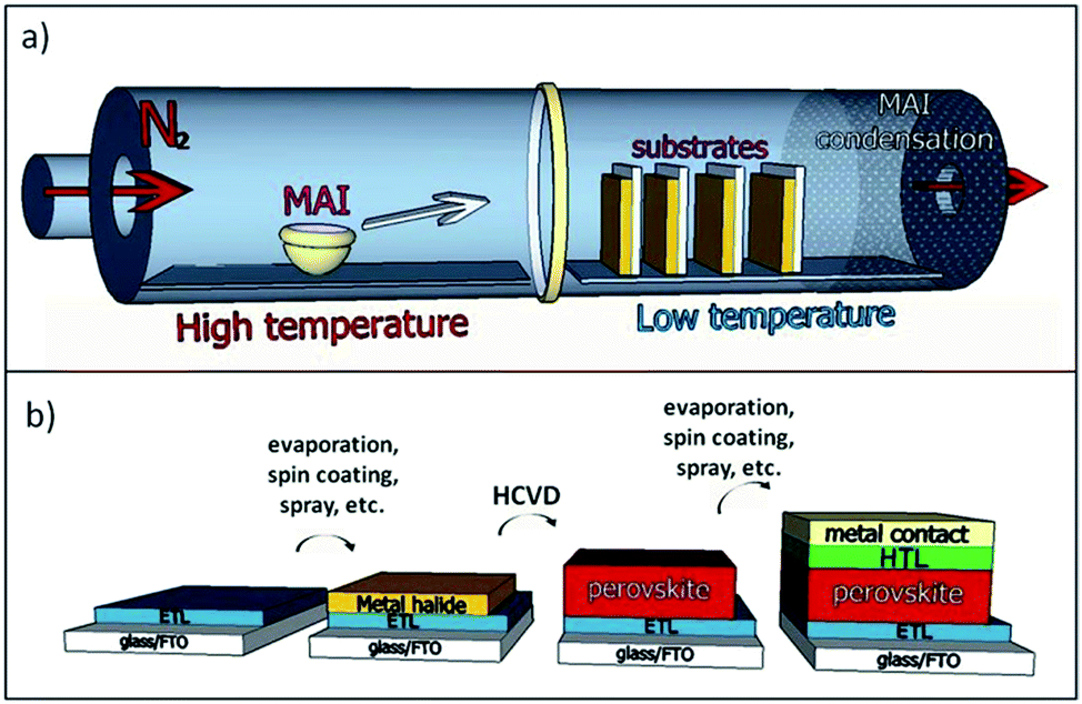 | ||
| Fig. 1 Hybrid chemical vapor deposition based perovskite synthesis (a) diagram of the HCVD furnace and MAI deposition onto metal halide seeded substrates. (b) Layered structure of a complete solar cell fabricated by a HCVD process. The complete solar cell is a glass substrate followed by a FTO layer, an electron transport layer, a perovskite layer, a hole transport layer, and a top metal contact. | ||
A schematic diagram of a complete solar cell and the layers within is shown in Fig. 1b. The electron transport layer (ETL) of the cell is FTO coated with a thin film of titanium oxide made by spray pyrolysis. This is followed by the deposition of a metal halide layer and HCVD perovskite synthesis. The hole transport layer (HTL) is a film of spiro-MeOTAD spun onto the perovskite surface followed by gold top electrode deposition via evaporation. A photograph of a complete, functioning device is shown in Fig. 2a. From this image, we can see that the film is partially transparent and homogeneous. The absorbance spectrum was taken on a complete device (Fig. 2b) and the absorption edge was measured to be at 781 nm (ref. 14) making it suitable for applications like photovoltaic windows and multi-junction solar cells.19
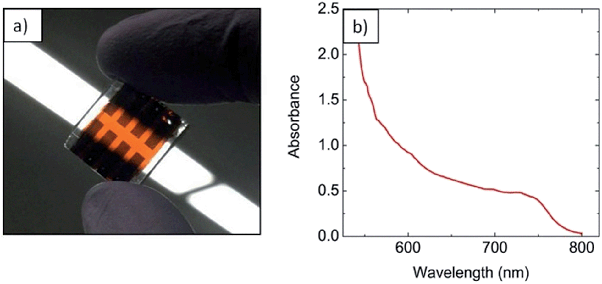 | ||
| Fig. 2 Transmission through the complete perovskite solar cell. (a) Back view of the complete HCVD solar cell with front illumination from a fluorescent light bulb; (b) UV-vis spectrum of a complete cell showing an absorption edge at 781 nm. | ||
The furnace zone with MAI was heated to 185 °C, and the zone with the substrate was heated to a nominal temperature of 130 °C. Due to the flow of hot gas, the temperature inside the growth region is a gradient between the two set temperatures. Specifically, substrates were usually loaded in the region that reaches a maximum temperature between 160 °C and 170 °C. Samples that were placed in a region hotter than 170 °C were not observed to correctly form perovskite. The initial PbCl2 layer was converted into a yellow film of PbI2 in the high temperature regions of the furnace (ESI, Fig. S1†). This suggests that the substrate temperature was too high, and that there is a maximum temperature of perovskite formation around 170 °C. Substrates that were loaded in zones with a maximum temperature of 145 °C were found to be unstable. Perovskite formed at this temperature rapidly turned transparent when exposed to air. Independent control of temperature zones and control of pressure provide significant advantages over existing vapor deposition methods.9 The additional degree of control may open the door for fabrication of a wider range of perovskite materials.
Thermal evaporation was used to deposit the metal halide layer because it offers good uniformity and thickness control. The resulting perovskite films show a relatively smooth morphology with complete coverage (RMS roughness = 28 ± 10 nm, on silicon). Fig. 3a and b show AFM images of perovskite films in true proportions (i.e., the lengths along the lateral and vertical directions have the same scale). This surface roughness is similar to the roughness of the FTO/TiO2 substrates used for solar cells (∼27 nm). A perovskite film on the FTO/TiO2 substrate was measured to have a roughness of ∼50 nm. In contrast, solar cells that are fabricated by a solution process often leads to incomplete coverage, and consequently a much higher roughness.20 Having lower surface roughness allows for thinner films on top of the perovskite, such as the hole transport layer and metal contact layer, which likely will lead to better optimized devices. Also in this work, the two top films correspond to the most expensive materials used, and having thinner films may help reduce manufacturing cost. The grains of perovskite films prepared by HCVD are typically between 0.2 and 2 μm in size, with an average size of approximately 0.6 ± 0.4 μm.
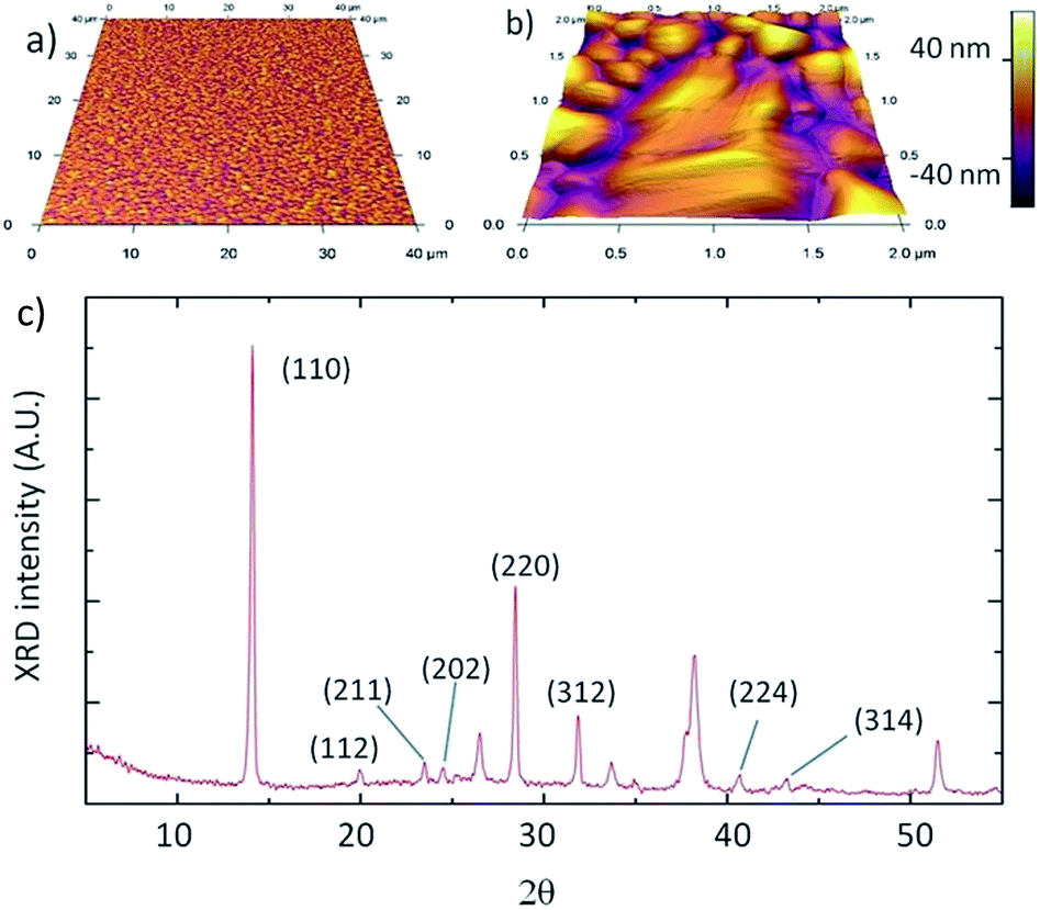 | ||
| Fig. 3 Analysis of perovskite films. (a and b) Atomic force microscopy 3D images of the perovskite thin film on the silicon substrate in true proportion. The silicon substrate was prepared under the same conditions and at the same time as those used for the highest performing device. (a) 40 × 40 μm2 scan of a perovskite film with 18 nm RMS roughness. (b) 2 × 2 μm2 image showing the laminate structure of the perovskite grains. (c) X-ray diffraction spectrum of the working perovskite solar cell. The major perovskite peaks (110) at 14.1°, and (220) at 28.4° are clearly shown. | ||
It appears that PbCl2 is mostly converted to perovskite during the CVD process. Film thicknesses are measured before and after the CVD deposition process and it is found to increase by a factor of 3.0 ± 0.2. It is possible to make an estimate of the thickness increase of fully converted perovskite assuming densities of lead chloride and perovskite to be 5.85 g cm−3 and 4.17 g cm−3, respectively.21 With these assumed densities, the expected volume would increase by a factor of 3.1, which is in good agreement with measured values and indicates that the perovskite is fully converted. Fig. 3c shows the X-ray diffraction (XRD) spectrum of the perovskite film and the observed characteristic diffraction peaks at 14° and 28.4° correspond to the (110) and (220) planes. The spectrum also reveals the presence of other orientations: (112) at 20.0°, (211) at 23.5°, (202) at 24.5°, (312) at 32.0°, (224) at 40.6, and (314) at 43.2°.22 There are also peaks associated with the substrate, which are predominately due to SnO and are found at 26.5°, 33.7°, 37.9°, and 51.5°. The relatively high intensity of peaks at orientations other than (110) and (220) suggests that perovskite films grown by HCVD are not highly oriented with respect to the substrate, which appears consistent with the AFM image in Fig. 3a. For some perovskite samples, X-ray diffraction spectra reveal a peak at 12.6° associated with the presence of PbI2. If present, these peaks are generally smaller compared to the main (110) perovskite peak, indicating that the resulting film mainly consists of perovskite.
One of the most important parameters observed is the thickness of the pre-deposited PbCl2 layer and subsequent perovskite. The average performance of solar cells with different PbCl2 layer thicknesses is shown in Fig. 4a. There appears to be a peak in efficiency at PbCl2 layer thickness approximately 100 nm, or approximately 300 nm of perovskite. It has recently been proposed that lower open-circuit voltage (Voc) and fill factor (FF) observed for solar cell devices with a perovskite film thickness in excess of 300 nm can be due to the low hole mobilities of the electron blocking layer.23 Alternatively, poor performance with thick films may be due to perovskite grains smaller than the thickness of the film.24 This trend is most clearly observed when considering the fill factor as a function of thickness (ESI, Fig. S2†). Furthermore, it was found that post annealing substrates in air rather than in N2 significantly improves Voc, short-circuit current density (Jsc), and FF. The surface morphology after air annealing was observed to be different than surfaces annealed in a N2 environment. It is very likely that the effect we observe in this work is similar to the solvent annealing effects as reported recently by Xiao et al.24 A set of air annealed solar cells, including the best performing cell demonstrated, is shown in Fig. 4b. This batch of solar cells had an average measured PbCl2 thickness of 103 ± 3 nm and an average measured perovskite thickness of 296 ± 4 nm. The devices from this batch annealed in N2 had an average efficiency of 6.1% and a maximum of 8.8%, while the devices annealed in air had an average efficiency of 10.8%, and a maximum of 11.8%.
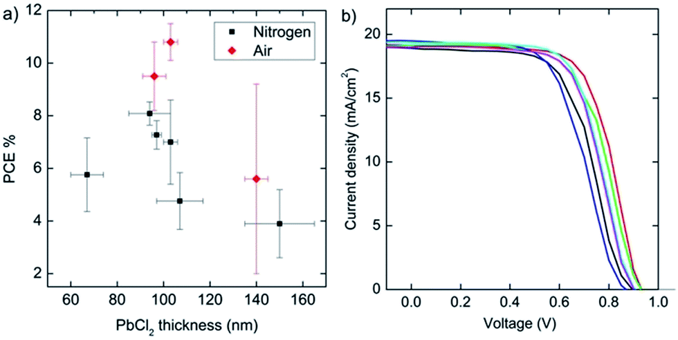 | ||
| Fig. 4 Perovskite solar cell performance. (a) Efficiency as a function of film thickness. Scatter plot of average efficiencies of solar cells at different seed layer thicknesses. Black dots represent cells that were annealed in N2 and the red diamonds represent cells that were annealed in air. (b) I–V measurements on the top performing batch of solar cells. The cells have ∼300 nm of perovskite grown by HCVD. The curves shown were measured ∼500 h after device fabrication. | ||
To monitor the stability of perovskite solar cells made by HCVD, some samples were measured after 450–1100 h of storage in a N2 glove box. On average, the cells maintained their efficiency (ESI, Fig. S3†). For example, the highest performing sample was measured about 1100 h after the initial measurement and was found to have similar efficiency to the original measurement. After 1100 h, the cell's Voc decreased slightly (−1%) but Jsc (+2%) and FF (+5%) increased. The solar cell performance measurements were performed in ambient air with a temperature of ∼25 °C and a relative humidity of ∼50%. Between the measurements, the samples were stored in the dark, inside a N2 glove box with H2O and O2 levels less than 0.1 ppm. The cell has spent a total of approximately 8 h outside of the N2 glove box for measurements. The stability observed in our solar cells is likely related to the fact that perovskite in our HCVD method reaches temperatures above 160 °C. At a temperature above 160 °C, excess MAI and incorporated water are expected to evaporate completely. The HCVD process forms perovskite with a constant flow of MAI and may be prone to absorb excess MAI. A film of MAI is hygroscopic and will likely cause instability issues. Thermogravimetric analysis shows that a MAI powder sample starts to lose mass at 145 °C (ESI, Fig. S4†). This is consistent with the observation that the minimum temperature of stable perovskite formation is higher than 145 °C.
Similar to perovskite solar cells that are fabricated with other methods, devices fabricated by HCVD suffer from hysteresis.22 The top performing cell showed substantially lower (7.0%) efficiency when measured in the reverse bias (ESI, Fig. S5†). Further optimization of parameters such as layer thickness, MAI deposition temperature and time, and annealing conditions could yield performance similar to those of the highest performing solar cells, but is beyond the scope of this study.
Experimental
Details involving synthesis, fabrication and measurement are included in the ESI.†Conclusions
To summarize, we developed a new method of perovskite synthesis by hybrid chemical vapor deposition (HCVD). The solar cells fabricated by this method not only achieved efficiencies as high as 11.8%, but also exhibited decent stability showing almost the same efficiency after approximately 1100 h storage in dry N2 gas. HCVD is of particular advantage due to its ability to scale up to industrial levels and the ability to precisely control gas flow rate, temperature, and pressure with high reproducibility. It is expected that process optimization of HCVD can further improve performance.Acknowledgements
The authors would like to acknowledge the financial support from the Okinawa Institute of Science and Technology Graduate University in Japan.References
- A. Kojima, K. Teshima, Y. Shirai and T. Miyasaka, J. Am. Chem. Soc., 2009, 131, 6050–6051 CrossRef CAS PubMed
.
- M. Liu, M. B. Johnston and H. J. Snaith, Nature, 2013, 501, 395–398 CrossRef CAS PubMed
- J. Burschka, N. Pellet, S.-J. Moon, R. Humphry-Baker, P. Gao, M. K. Nazeeruddin and M. Grätzel, Nature, 2013, 499, 316–319 CrossRef CAS PubMed
- J. T.-W. Wang, J. M. Ball, E. M. Barea, A. Abate, J. A. Alexander-Webber, J. Huang, M. Saliba, I. Mora-Sero, J. Bisquert, H. J. Snaith and R. J. Nicholas, Nano Lett., 2014, 14, 724–730 CrossRef CAS PubMed
- C.-H. Chiang, Z.-L. Tseng and C.-G. Wu, J. Mater. Chem. A, 2014 10.1039/C4TA03674C
- H. Zhou, Q. Chen, G. Li, S. Luo, T. Song, H.-S. Duan, Z. Hong, J. You, Y. Liu and Y. Yang, Science, 2014, 345, 542–546 CrossRef CAS PubMed
- H. Hu, D. Wang, Y. Zhou, J. Zhang, S. Lv, S. Pang, X. Chen, Z. Liu, N. P. Padture and G. Cui, RSC Adv., 2014, 4, 28964–28967 RSC
- J. Burschka, N. Pellet, S.-J. Moon, R. Humphry-Baker, P. Gao, M. K. Nazeeruddin and M. Grätzel, Nature, 2013, 499, 316–319 CrossRef CAS PubMed
- Q. Chen, H. Zhou, Z. Hong, S. Luo, H.-S. Duan, H.-H. Wang, Y. Liu, G. Li and Y. Yang, J. Am. Chem. Soc., 2014, 136, 622–625 CrossRef CAS PubMed
- Z. Xiao, C. Bi, Y. Shao, Q. Dong, Q. Wang, Y. Yuan, C. Wang, Y. Gao and J. Huang, Energy Environ. Sci., 2014 10.1039/C4EE01138D
- D. Bi, S.-J. Moon, L. Häggman, G. Boschloo, L. Yang, E. M. J. Johansson, M. K. Nazeeruddin, M. Grätzel and A. Hagfeldt, RSC Adv., 2013, 3, 18762 RSC
- S. T. Ha, X. Liu, Q. Zhang, D. Giovanni, T. C. Sum and Q. Xiong, Adv. Opt. Mater., 2014, 2, 838–844 CAS
- D. J. Lewis and P. O'Brien, Chem. Commun., 2014, 50, 6319–6321 RSC
- H.-S. Kim, C.-R. Lee, J.-H. Im, K.-B. Lee, T. Moehl, A. Marchioro, S.-J. Moon, R. Humphry-Baker, J.-H. Yum, J. E. Moser, M. Grätzel and N.-G. Park, Sci. Rep., 2012, 2 DOI:10.1038/srep00591
-
X.-T. Yan and Y. Xu, Chemical Vapour Deposition: An Integrated Engineering Design for Advanced Materials, Springer Science & Business Media, 2010 Search PubMed
- S. Colella, E. Mosconi, P. Fedeli, A. Listorti, F. Gazza, F. Orlandi, P. Ferro, T. Besagni, A. Rizzo, G. Calestani, G. Gigli, F. De Angelis and R. Mosca, Chem. Mater., 2013, 25, 4613–4618 CrossRef CAS
- H. Yu, F. Wang, F. Xie, W. Li, J. Chen and N. Zhao, Adv. Funct. Mater., 2014 DOI:10.1002/adfm.201401872
-
H. Mehrer, Diffusion in Solids: Fundamentals, Methods, Materials, Diffusion-Controlled Processes, Springer Science & Business Media, 2007 Search PubMed
- G. E. Eperon, V. M. Burlakov, A. Goriely and H. J. Snaith, ACS Nano, 2014, 8, 591–598 CrossRef CAS PubMed
- A. Dualeh, N. Tétreault, T. Moehl, P. Gao, M. K. Nazeeruddin and M. Grätzel, Adv. Funct. Mater., 2014 DOI:10.1002/adfm.201304022
- D. Weber, Z. Naturforsch., B: Anorg. Chem., Org. Chem., 1978, 33, 1443–1445 Search PubMed
- N. J. Jeon, J. H. Noh, Y. C. Kim, W. S. Yang, S. Ryu and S. I. Seok, Nat. Mater., 2014, 13, 897–903 CrossRef CAS PubMed
- C. Momblona, O. Malinkiewicz, C. Roldán-Carmona, A. Soriano, L. Gil-Escrig, E. Bandiello, M. Scheepers, E. Edri and H. J. Bolink, APL Mater., 2014, 2, 081504 CrossRef PubMed
- Z. Xiao, Q. Dong, C. Bi, Y. Shao, Y. Yuan and J. Huang, Adv. Mater., 2014 DOI:10.1002/adma.201401685
Footnote |
| † Electronic supplementary information (ESI) available. See DOI: 10.1039/c4ta04385e |
| This journal is © The Royal Society of Chemistry 2014 |