
 Open Access Article
 This Open Access Article is licensed under a
 Creative Commons Attribution 3.0 Unported Licence
Ionic conductivity of YSZ/CZO multilayers with variable lattice mismatch
Weida
Shen
*a and
Joshua L.
Hertz
ab
aDepartment of Mechanical Engineering, University of Delaware, 126 Spencer Laboratory, Newark, DE 19716, USA. E-mail: weida@udel.edu; Fax: +1 302 831 3619; Tel: +1 302 831 8452
bDepartment of Materials Science and Engineering, University of Delaware, 201 DuPont Hall, Newark, DE 19176, USA
First published on 5th December 2014
Abstract
Heterostructured multilayers have been controversially reported to alter the oxygen ion conductivity of solid electrolytes by inducing interfacial mechanical strain. Here, we fabricated thin film multilayers composed of 9 mol% Y2O3 doped ZrO2 (YSZ) and Ce1−xZrxO2 (CZO) to systematically quantify the effects of tensile strain on the oxygen-ion conduction behavior in YSZ. A significant advantage of using CZO is that its lattice parameter can be continuously varied by adjusting the Ce/Zr atomic ratio, simplifying the strain control over the neighboring YSZ layers. Three different sets of multilayers composed of YSZ with CeO2, or with Ce0.70Zr0.30O2 (CZO30), or with Ce0.55Zr0.45O2 (CZO45) were prepared on Al2O3 substrates with interfacial lattice mismatch of +5.2%, +3.7%, and +2.9%, respectively. When decreasing the individual layer thicknesses from 35 nm to 5 nm, all of the multilayers exhibited little change of the conductivity, with values consistently near that of bulk YSZ. X-ray diffraction results indicate that the interfacial strains were largely relaxed. Suggestions that multilayers are unable to effect ionic conductivity changes must therefore consider the difficulties in obtaining lattice mismatch-based elastic strain, even at <3% mismatch.
1. Introduction
ZrO2-based materials have been widely used as the electrolyte for solid oxide fuel cells (SOFCs) due in part to their very high mechanical and chemical durability.1–3 The most representative and best known example is yttria-stabilized zirconia (YSZ).4 Traditionally processed ceramic YSZ achieves sufficient oxygen ion conductivity (0.01 S cm−1) for SOFC operation at temperatures over 800 °C.1 This extremely high operating temperature decreases cell durability and increases component cost. In order to decrease the operating temperatures of SOFCs to 500 °C, one of the most important requirements is to increase the low temperature oxygen ion conductivity of the electrolyte. With the rapid development of thin film fabrication techniques, numerous recent reports have been focused on the study of nanostructured multilayers or heterostructures for solid electrolytes.5–10 The unique interfacial effects between two oxides may have the capability to significantly alter the oxygen ion transport properties.Azad et al. reported that conductivity increased by at least one order of magnitude in Gd2O3-doped ZrO2/Gd2O3-doped CeO2 multilayers as the thicknesses of the individual layers decreased to 15 nm.11 Later studies by Sanna et al.12 and Li et al.13 observed similar increases in conductivity with increasing interfacial density in multilayers composed of YSZ with Ce0.8Sm2O2−δ and YSZ with Gd2Zr2O7, respectively. The defect concentration in the doped ZrO2 and doped CeO2 layers are relatively large such that any space charge regions at the multilayer interfaces are inconsequently small, approximately ≈1 Å.14 Ion redistribution at the interfaces would thus have little impact on the overall defect concentrations or, therefore, oxygen ion conductivities. Instead, interfacial structures such as lattice mismatch strain were presumed to have altered the mobility of existing defects.
A systematic study of the effects of lattice mismatch strains on oxygen ion transport properties was reported previously.15–18 Multilayers were composed of 9.5 mol% YSZ and various insulating rare earth oxides (e.g., Y2O3, Lu2O3, and Sc2O3). Unlike the previous studies,11–13 the rare earth oxides support little oxygen ion conductivity so that only the varying strain state in the YSZ layers would be expected to affect the measured oxygen ion conduction behavior of the multilayer structure. The interfacial conductivity of the structures was found to have a log-linear dependence on the amount of strain induced in the YSZ layers. Biaxial tensile strain in the YSZ layers increased the ionic conductivity, while compressive strain decreased it. This finding was in good agreement with a theoretical model based on the pressure dependence of the free energy for vacancy migration.
Other reports have suggested less effect from lattice-mismatched multilayers. Pergolesi et al. studied multilayers composed of YSZ and pure CeO2 with a lattice mismatch of ≈+5% at interfaces.19 The putative tensile strain induced in the YSZ, however, had no effect on the oxygen ion conduction, even when the individual layer thicknesses were decreased to 5 nm. Garcia-Barriocanal et al. claimed conductivity enhancement by eight orders of magnitude in YSZ/SrTiO3 multilayers.20 This increase was attributed to large tensile strain (≈7%) in the YSZ layers, but evidence from ongoing experiments suggest that electronic conduction through the SrTiO3 may be the true cause of the measured increases in total conductivity.21–23
In this work, we have fabricated multilayers composed of 9 mol% YSZ and Ce1−xZrxO2 (CZO) to study the ability to create tensile strain in YSZ-based multilayers. A significant advantage of using CZO as the strain-inducing material is that it has a lattice parameter that can be continuously varied by adjusting the Ce/Zr atomic ratio. CZO adopts cubic and/or tetragonal structures when the Zr content, x, is less than 0.5.24–26 The lattice parameters of cubic and tetragonal CZO (x ≤ 0.5) are nearly the same, such that the X-ray diffraction patterns of these phases are very difficult to distinguish.26 The existence of tetragonal phase CZO does not affect its use as a means to create lattice mismatch. The similarity in crystal structure of CZO with YSZ increases the likelihood of creating epitaxial, coherently-strained multilayer thin films. Previous work by the authors developed a unique film fabrication method that provides compositional control within the Y2O3–ZrO2–CeO2 solid solution space at the single nanometer level.27 This method was used recently to quantify a significant reduction in ionic conductivity with increasing biaxial compression in multilayers of CZO and yttria-doped ceria (YDC).28 Here, we use highly analogous experimentation to examine if CZO can be used to create increased ionic conductivity via biaxial tension in neighboring YSZ layers.
2. Experimental
Thin films were reactively sputtered from single element targets of Ce, Zr, and Y (ACI Alloys, San Jose, CA) in a multi-target, magnetron sputtering machine (PVD Products, Wilmington, MA). Before film deposition, the main sputtering chamber was evacuated to a background pressure less than 1.33 × 10⁻⁵ Pa (10−7 Torr). Working gasses of Ar and O2 were introduced into the sputtering chamber at a total flow rate of 20 sccm with an Ar/O2 ratio of 9![[thin space (1/6-em)]](https://www.rsc.org/images/entities/char_2009.gif) :1 and a working pressure of 1.33 Pa (10 mTorr). Single crystal Al2O3 (0001) substrates (10 mm × 10 mm × 0.5 mm) were heated to 650 °C for film growth. The details of the calibration of deposition rate and film composition were reported previously.27
:1 and a working pressure of 1.33 Pa (10 mTorr). Single crystal Al2O3 (0001) substrates (10 mm × 10 mm × 0.5 mm) were heated to 650 °C for film growth. The details of the calibration of deposition rate and film composition were reported previously.27
Multilayer thin films were deposited using a software module controlling this sputtering system. Layers were sputtered sequentially with a control program that determined the power applied to each target and/or the toggling of desired target shutters. The details of characterization and verification of the multilayer structures were reported previously by the authors.14
The orientations of the films and their out-of-plane lattice parameters were characterized by θ–2θ X-ray diffraction (XRD) measurements in a Philip X'Pert diffractometer with Cu Kα radiation. Platinum interdigitated electrodes, as shown in Fig. 1, were fabricated on the surface of films by lift-off photolithography. The width and separation distance of the electrodes were each 100 μm with a total electrode perimeter length of ≈115 mm. Impedance spectra were measured in air using a Novocontrol Alpha-A analyzer with a signal voltage of 10 mV and frequency range between 1 Hz and 3 MHz. Before measurement, samples were first heated in air to 650 °C. The impedance data used to calculate the film conductivity were stable upon repeatedly cycling the temperature up to 650 °C and then measuring every 50 °C as the temperature decreased.
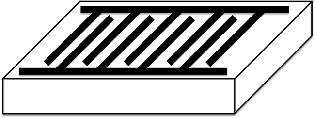 | ||
| Fig. 1 Platinum interdigitated electrode pattern deposited on the top surface of film for impedance measurement. The width and inter-space of the electrode fingers were both kept at 100 μm. The total perimeter length of the electrodes was ≈115 mm. | ||
Recently, there is a concern of using electrodes deposited on the top surface of film to measure the resistance of the whole multilayer. Schweiger et al. used two different types of electrode structures to measure the electrical impedance of Ce0.9Gd0.1O2−δ/Er2O3 multilayers.29 By using electrodes deposited on the side of the multilayers, the conductivity was found to be gradually decreased by at least one order of magnitude when the number of Ce0.9Gd0.1O2−δ/Er2O3 interfaces increased, but for the electrode pattern deposited on the top surface of the multilayers, the conductivity was nearly constant. Since the resistance of the Er2O3 layer was much larger compared to that of Ce0.9Gd0.1O2−δ, the electrical current was considered unable to penetrate into the whole multilayer for the electrodes deposited on the top surface and the current was blocked by the second insulating layer of Er2O3. The measured impedance was attributed to the electrical conduction through the top or the first Ce0.9Gd0.1O2−δ layer, resulting similar effective conductivity even when the number of strained interfaces increased.
In this work, we used CZO as the second phase to induce different lattice mismatches at the interfaces between YSZ and CZO layers. The electrical conductivity of the rare earth oxides (e.g., Y2O3, Gd2O3, and Er2O3) is much smaller. For example, at 727 °C, the electrical conductivity of Gd2O3 was only on the order of 10−6 S cm−1.30 On the other hand, the electrical conductivity of CZO was not so small and in the order of 10−4 S cm−1 at 650 °C.31 This conductivity value was about 1.5 orders of magnitude less than that of YSZ at the same temperature. These CZO layers, therefore, are not so highly resistive as to block the current path from penetrating through the entire thickness of the multilayer. The current in this work was considered not to remain confined just to the top or the first layer of YSZ.
3. Results and discussion
Three different sets of multilayers composed of 9 mol% YSZ with CeO2, with Ce0.70Zr0.30O2 (CZO30), or with Ce0.55Zr0.45O2 (CZO45), were prepared. The lattice parameter of CZO obeys Vegard's law with a linear dependence on Zr content.32 Based on the lattice parameters of YSZ (≈5.14 Å (ref. 33)) and CeO2 (≈5.41 Å (ref. 34)), the lattice parameters of CZO30 and CZO45 solid solutions can be estimated as 5.33 Å and 5.29 Å, respectively. Since the lattice parameters of these CeO2–ZrO2 solid solutions are larger compared to that of YSZ, an in-plane tensile strain is ostensibly induced in YSZ layers near the interfaces in YSZ/CZO multilayers. The two constituent materials YSZ and CZO have closely related lattice symmetry, so the lattice mismatch at the interface, f, is calculated as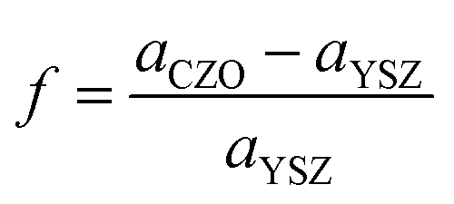 | (1) |
Ceria-based materials often exhibit polycrystalline structure on Al2O3 due to the large lattice mismatch between substrate and film.36,37 On the other hand, YSZ films have exhibited nearly epitaxial growth on c-plane Al2O3 substrates in our previous work.38 A 5 nm-thick YSZ was deposited first as a buffer layer to create epitaxial growth of the multilayer. The structure of the multilayer films can be described as
| Al2O3—YSZ (5 nm-thick)—CZO—(YSZ—CZO) × N |
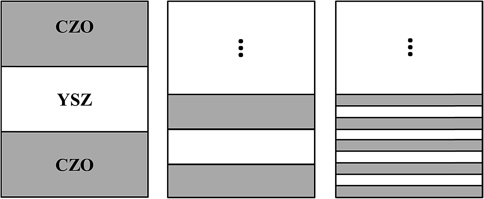 | ||
| Fig. 2 Schematic structure of the multilayer films composed of alternating layers of YSZ and CZO above the 5 nm-thick YSZ buffer layer. | ||
| Sample | CZO layer thickness (nm) | YSZ layer thickness (nm) | Number of bilayers (N) |
|---|---|---|---|
| N = 1 | 35 | 35 | 1 |
| N = 3 | 15 | 15 | 3 |
| N = 10 | 5 | 5 | 10 |
Fig. 3(a) shows the XRD patterns of the YSZ/CeO2 multilayers on Al2O3 (0001) substrates. Single-layer YSZ and CeO2 thin films with thickness of ≈105 nm are included for comparison. The single layer CeO2 thin film exhibits both (111) and (100) orientations, but the single layer YSZ film and all of the YSZ/CeO2 multilayers (which had the YSZ buffer layer) are highly textured along the (111) direction. The out-of-plane lattice parameters of YSZ and CeO2 single-layer thin films calculated from the (111) diffraction locations were 5.21 Å and 5.41 Å, respectively. The lattice parameter of the CeO2 thin film was almost the same as that of the bulk value, indicating that the film was fully relaxed on the Al2O3 substrate due to the very large lattice mismatch. For the single-layer YSZ thin film, the out-of-plane lattice parameter, however, exceeded the bulk value of 5.14 Å, an effect noted previously.38 Since this value is larger than the bulk value by about 1.3%, a roughly 0.6% biaxial in-plane compressive strain (value estimated from an assumption of zero net lattice volume change) was presumed in the YSZ single-layer film due to the interface with the Al2O3 substrate.
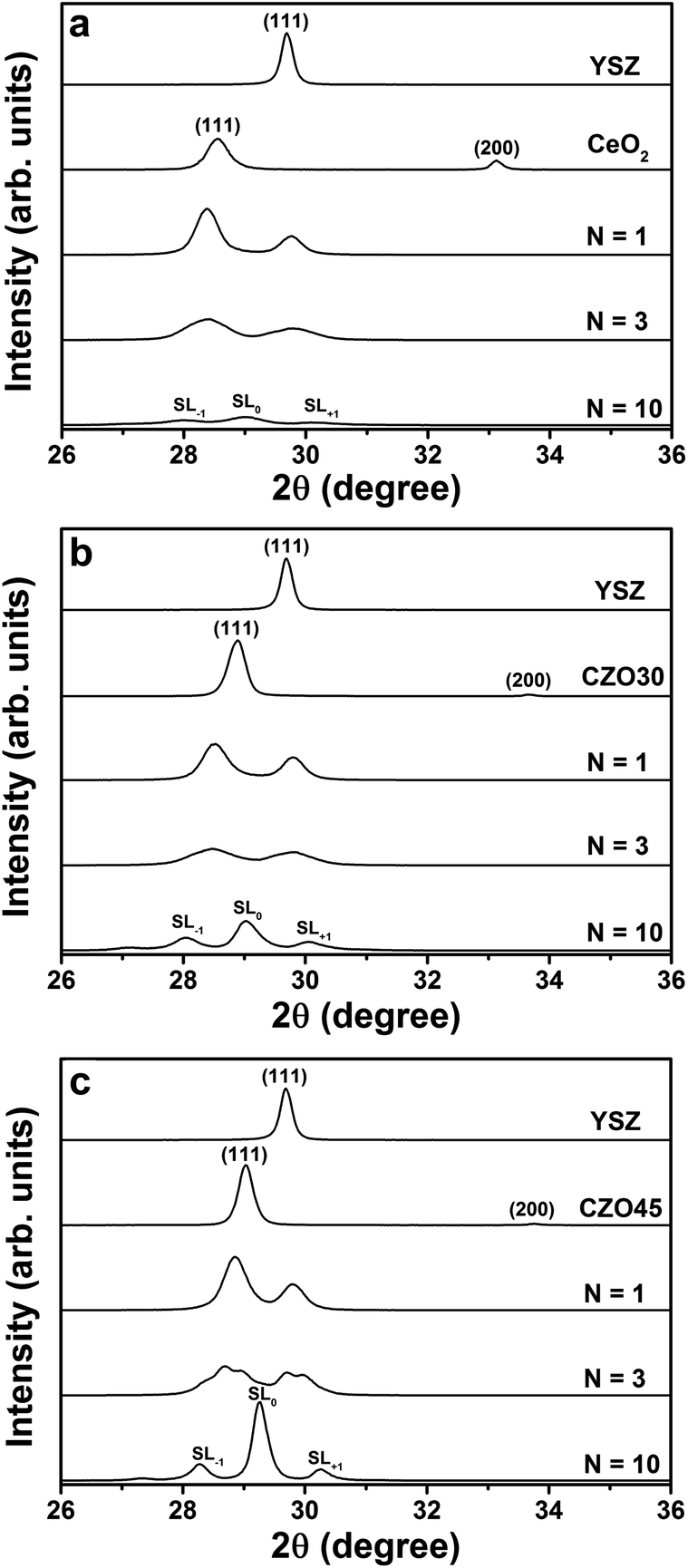 | ||
| Fig. 3 XRD patterns of multilayer thin films composed of N bilayers of (a) YSZ and CeO2, (b) YSZ and CZO30, and (c) YSZ and CZO45. The corresponding single-layer YSZ and CZO thin films deposited on Al2O3 (0001) with thickness of ≈105 nm were also included for comparison. | ||
For N = 1, the multilayer exhibits two separate diffraction peaks representing the planes of YSZ (111) and CeO2 (111). The peak locations correspond to out-of-plane lattice parameters of 5.20 Å for YSZ and 5.44 Å for CeO2. These values, therefore, represent a very slight reduction in lattice parameter for YSZ (111) and slight dilation for CeO2 (111) in the out-of-plane direction. As the individual layer thickness decreased to 15 nm for the N = 3 multilayer, the peak locations did not significantly shift compared to the locations of N = 1. A superlattice pattern composed of an average structural peak SL0 surrounded by two first-order satellite peaks SL−1 and SL+1 is observed for N = 10. The average lattice parameter based on the SL0 peak was calculated to be 5.33 Å, which is in agreement with the average value of the out-of-plane lattice parameters of YSZ (5.20 Å) and CeO2 (5.44 Å).
Fig. 3(b) shows the XRD patterns of the YSZ/CZO30 multilayers. The out-of-plane lattice parameter of the single-layer CZO30 film was calculated to be 5.35 Å, which was also slightly larger than that of the bulk material (5.33 Å). Similar to what was found in the YSZ/CeO2 multilayers, the multilayer films exhibit (111) texture and transit from two distinct peaks to a superlattice pattern as the individual layer thicknesses decreased to 5 nm. For both the N = 1 and N = 3 multilayers, the out-of-plane lattice parameters were calculated to be 5.19 Å for YSZ and 5.42 Å for CZO30 (which was an increase from 5.35 Å for the CZO30 single layer film). These values again represent little effective mismatch strain created in the YSZ. For the N = 10 multilayer, the average lattice parameter based on the SL0 peak was calculated to be 5.33 Å, which is again similar to the average value (≈5.31 Å) of the out-of-plane lattice parameters of YSZ and CZO30.
The XRD patterns of the multilayers composed of YSZ and CZO45 are shown in Fig. 3(c). The out-of-plane lattice parameter of the single-layer CZO45 film was increased from 5.29 Å to 5.32 Å due to the substrate effect. For N = 1, the out-of-plane lattice parameter for YSZ was calculated to 5.19 Å, the same as that in YSZ/CZO30 multilayer. The lattice parameter of CZO45 in the multilayer film was 5.35 Å, an increase from 5.32 Å as a single-layer film. The two peaks start to transition to a superlattice pattern for the N = 3 multilayer. In this sample, the lattice parameter based on the CZO45 peak increased to 5.38 Å, but the value for YSZ remained 5.19 Å. A strong superlattice pattern is found for the N = 10 multilayer. The average lattice parameter calculated based on the SL0 peak was 5.29 Å, which is again similar to the computed average of the lattice parameters of the constituent layers, YSZ and CZO45.
Table 2 compares the out-of-plane lattice parameters of YSZ and CZO in bulk, single-layer films, and N = 1 and N = 3 multilayers. The bulk lattice parameters for CZO30 and CZO45 were calculated based on the Vegard's law, as discussed before. The out-of-plane lattice parameters of the YSZ across all three sets of multilayers were very similar to that of the single-layer film, ranging between 5.20 Å and 5.19 Å. The coupling of CZO with YSZ has insignificant effects on the YSZ lattice parameter. Thus, the interfacial strains in YSZ layers in YSZ/CZO multilayers were largely or fully relaxed. At the same time, the out-of-plane lattice parameters of the CZO gradually increased from the single-layer films to the N = 1 and N = 3 multilayers. Similar to the substrate effect noted previously for YSZ, the single-layer CZO30 and CZO45 films exhibited larger out-of-plane lattice parameters compared to that of the bulk materials. The single layer CeO2 film had a lattice parameter that matched the bulk value. By increasing the bilayer number from N = 1 to N = 3, the out-of plane lattice parameters of the CZO all gradually increased. These results indicate that the creation of tensile strains in the YSZ layers was much more difficult compared to the creation of compressive strains in the CZO layers.
| Sample | YSZ/CeO2 | YSZ/CZO30 | YSZ/CZO45 | |||
|---|---|---|---|---|---|---|
| YSZ | CeO2 | YSZ | CZO30 | YSZ | CZO45 | |
| Bulk | 5.14 Å | 5.41 Å | 5.14 Å | 5.33 Å | 5.14 Å | 5.29 Å |
| Single layer | 5.21 Å | 5.41 Å | 5.21 Å | 5.35 Å | 5.21 Å | 5.32 Å |
| N = 1 | 5.20 Å | 5.44 Å | 5.19 Å | 5.42 Å | 5.19 Å | 5.35 Å |
| N = 3 | 5.20 Å | 5.45 Å | 5.19 Å | 5.43 Å | 5.19 Å | 5.38 Å |
Previous work by the authors on multilayers of YDC and CZO found that as the individual layer thickness decreased, a superlattice diffraction pattern appeared and then, upon further thickness reduction to 5 nm, almost gave way to a single, sharp, very high-intensity peak.28 This indicated that the whole multilayer could be characterized by a single lattice parameter and that the YDC layers were effectively being compressively strained from the CZO layers. In this work, two distinct peaks remain for the N = 3 multilayers, and a superlattice pattern remains with satellite peaks clearly identified for the N = 10 multilayers. These results give clear indication that two distinct lattice parameters remain even for the thinnest individual layer thickness of 5 nm.
Moreover, the appearance of clear and sharp satellite peaks indicates the formation of high-quality, well-defined interfaces between the constituent layers.12 Nevertheless, the intensity of the SL0 peak of the YSZ/CeO2N = 10 multilayer is much smaller than that of the corresponding YSZ/CZO30 and YSZ/CZO45 multilayers, indicating relatively rougher or otherwise less ideal interfaces where the lattice mismatch is very large. The satellite peak angular locations allow direct calculation of the bilayer thickness according to
 | (2) |
Fig. 4 shows typical impedance spectra, from a YSZ/CZO45 (N = 10) multilayer at three different temperatures. At each temperature, the spectrum consists of a semicircle at high frequency and the beginning of a second semicircle at low frequency. Two R-CPE elements connected in series were used as the equivalent circuit to fit the impedance spectra. An additional resistance, RYSZ, in the equivalent circuit represents the resistance of the 5 nm-thick YSZ buffer layer. The value of RYSZ was fixed at each temperature and calculated based on the electrode geometry and conductivities obtained from a single layer YSZ thin film (≈105 nm). Resistance RYSZ was always at least one order of magnitude greater than R1. The equivalent capacitance of the constant phase element for the high frequency semicircle, CPE1, was found to be of order 10−11 F. This value is as low as can be measured in the experimental setup, and represents a stray capacitance in parallel with the sample under test. The equivalent capacitance value of CPE2 for the low frequency semicircle was at least four orders of magnitude larger, which is much too large to be due to conduction between the electrodes. This result clearly indicates that resistance R1 was due to conduction through the film eliminating the contribution from the 5 nm-thick YSZ buffer layer, while R2 was due to electrode polarization.
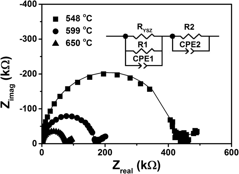 | ||
| Fig. 4 Impedance spectra measured in open air of YSZ/CZO45 multilayers with N = 10 at the temperatures indicated. Also shown is the equivalent circuit used to fit the data (RYSZ was a fixed value at each temperature). | ||
Fig. 5 shows the fitted resistance of R1 as a function of the individual layer thickness in YSZ/CZO30 multilayers at 650 °C. As mentioned before, for electrodes deposited on the top surface of film, there is a concern of measuring just the impedance of the first YSZ layer. If we assume this concern is true, then as the top layer thickness of YSZ decreased from 35 nm to 5 nm in the multilayers, the fitted resistance of R1 for the whole multilayers needs to be gradually increased. The measured resistance for the multilayers with 5 nm-thick YSZ should be 3 times larger than that in multilayers with 15 nm-thick YSZ, and 7 times larger than that in multilayers with 35 nm-thick YSZ. In reality, as shown in Fig. 5, the fitted resistance of R1 was nearly constant when the individual thickness decreased from 35 nm to 5 nm. For the other two types of multilayers composed of YSZ with CeO2 or with CZO45, the fitted resistance R1 was also found to be essentially independent of the individual layer thickness. These findings indicated that the measurement current was not just confined to the top or the first YSZ layer, but penetrating into the whole multilayer.
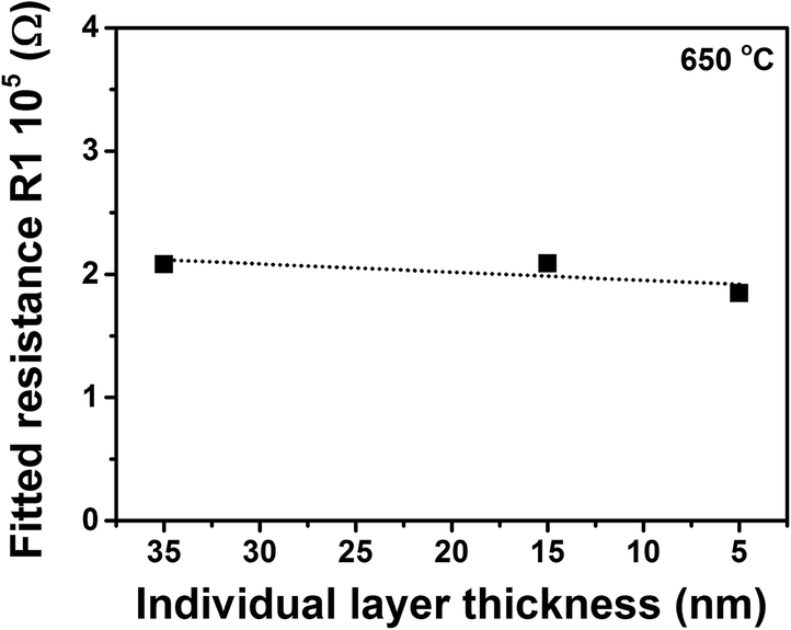 | ||
| Fig. 5 The fitted resistance R1 of YSZ/CZO30 multilayers as a function of the individual layer thickness at 650 °C. | ||
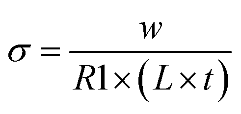
The undoped CeO2 possesses relatively low oxygen ion conductivity, on the order of 10−3 at 650 °C.39 The addition of Zr into CeO2 to form CZO further decreases the conductivity due to the reduced vacancy mobility.40 The electrical conductivity of the CZO, therefore, is at least one order of magnitude less compared to that of YSZ. The contributions from the CZO and 5 nm thick YSZ buffer layer to the overall electrical conduction can be likely neglected. The overall conductivity of the multilayers in this work, σ, was calculated based on R1, the electrode geometry, and the total thickness of YSZ within the multilayer according to the equation of
 | (3) |
Fig. 6 compares the oxygen ion conductivity of the 105 nm-thick YSZ single-layer film studied in this work with a single YSZ substrate measured in our lab. The activation energies (determined from the σT product) are also included in the figure. The Y2O3-dopant concentration in these two materials was similar, about 8–9 mol%. The conductivity of the single-layer film was found to be about 0.25 orders of magnitude less compared to that of the single crystal. One of the possible causes for the decreased conductivity for the YSZ thin film may be due to the compressive strain exerted by the substrate, as discussed in the XRD analysis. Moreover, the single-layer and multilayer YSZ films likely adopted a columnar microstructure. Grain boundaries are well known to depress ionic conductivity in YSZ.
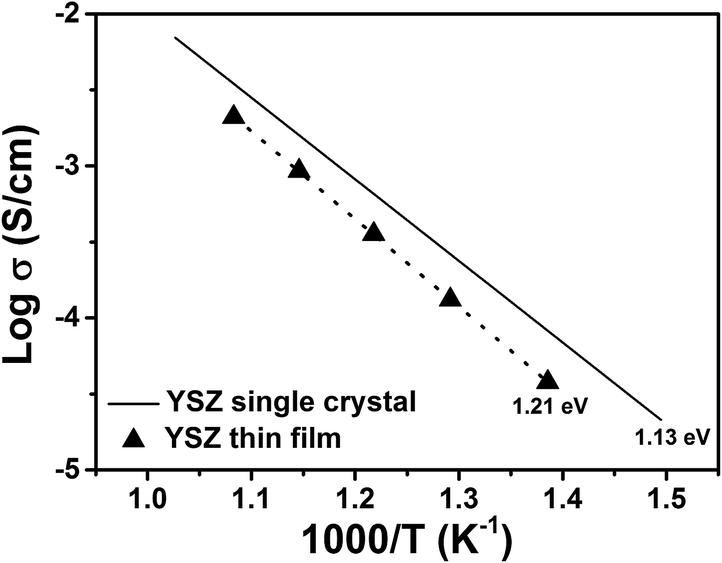 | ||
| Fig. 6 Comparison of electrical conductivity between a 105 nm-thick YSZ single-layer film and a roughly 500 μm-thick single crystal YSZ bulk sample. | ||
The single layer and multilayer YSZ films are believed to have adopted similar columnar structures, and thus any effects of the existence of grain boundaries would be felt across all of the measured films. It is possible that the effects of tensile strain that we seek to find in this study could be masked by a grain boundary conductivity that is both very low and unaffected by strain. However, no such difficulties plagued the previous, highly parallel study in ref. 28, where both grain boundaries and strain effects were conclusively found.
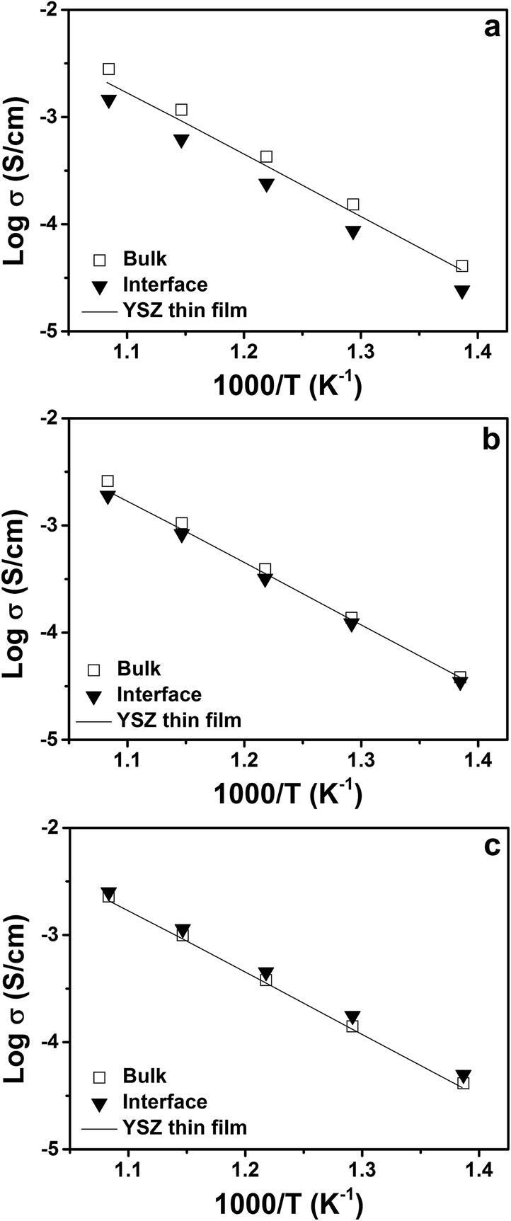
Fig. 7(a) shows Arrhenius plots of the electrical conductivity of YSZ/CeO2 multilayers measured in air. The conductivity of a single layer YSZ thin film with thickness of ≈105 nm is included for comparison. From the figure, we can see that the electrical conductivities for N = 1 and N = 3 have similar values compared to that of the YSZ thin film. The electrical conductivity for N = 10, however, is slightly reduced by a factor of ≈2. These results compare very well to those reported by Pergolesi et al.19 on a similar study of multilayers composed of YSZ and CeO2. In that study, the authors found no change in conductivity of YSZ even with individual layer thickness decreased to 5 nm. The slightly decreased conductivity for N = 10 in this work, similar to what was found in our previous study of YDC/CeO2 multilayers, may be due to non-zero roughness at the interfaces.28 As shown in Fig. 3, the YSZ/CZO multilayers with smallest layer thicknesses exhibited typical superlattice XRD patterns consisting of an average diffraction peak SL0 surrounded by two satellite peaks SL+1 and SL−1. The appearance of clear and sharp satellite peaks indicates the formation of high-quality, well-defined interfaces between two constituent layers. The intensity of the satellite peaks of the YSZ/CeO2 multilayer for N = 10, however, were much smaller, broader, and less well defined than that of the corresponding YSZ/CZO30 and YSZ/CZO45 multilayers. All of these findings support our conclusion that the YSZ/CeO2 interfaces were relatively rougher, likely due to the very large lattice mismatch.
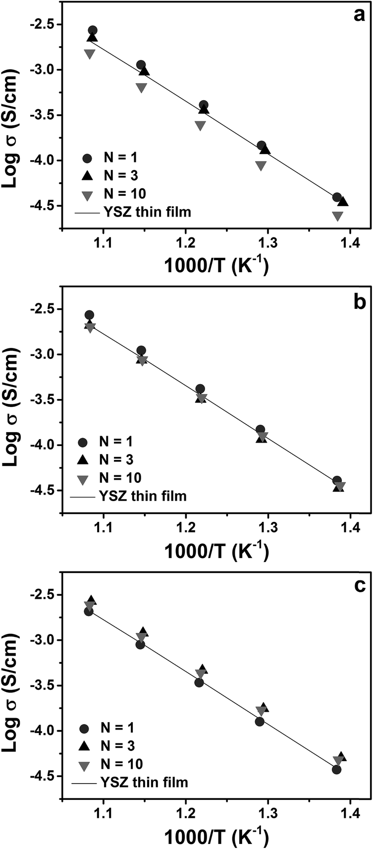 | ||
| Fig. 7 Arrhenius plots of the electrical conductivity of the YSZ layers in the (a) YSZ/CeO2, (b) YSZ/CZO30, and (c) YSZ/CZO45 multilayers. Shown for comparison is the conductivity measured from a single-layer YSZ film with thickness of ≈105 nm. | ||
Fig. 7(b) and (c) show Arrhenius plots of electrical conductivity of the YSZ/CZO30 and YSZ/CZO45 multilayers, respectively. In both cases, as the individual layer thickness decreased from 35 nm (N = 1) to 5 nm (N = 10), the multilayers exhibit nearly identical conductivities as that of the YSZ single-layer thin film. The decreased interfacial lattice mismatch in these multilayers relative to the YSZ/CeO2 multilayers seems to increase the interface quality for N = 10, resulting in similar conductivities with those of the N = 1 and N = 3 multilayers.
The conduction behavior of the multilayers can be better understood by deconvoluting the conduction paths through the YSZ layers into two independent, parallel parts.41 The first pathway is through the volume or bulk region, and the second pathway is through the region close to the interface. The relationship between the total conductivity and the volume and interfacial conductivities is derived as41
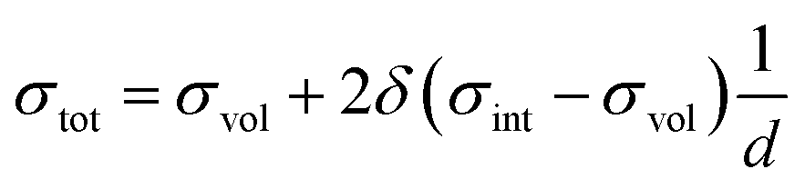 | (4) |
Fig. 8 shows conductivity isotherms at 650 °C for the three sets of multilayers as a function of the reciprocal layer thickness. Based on eqn (4), a linear fit of the total conductivity as a function of 1/d allows us to deconvolute the volume and interfacial conductivities. In our previous study of YDC/CZO multilayers, the total conductivity reduced in a roughly log-linear fashion as the individual layer thickness decreased to 5 nm, and so the interfacial region was assumed to be around 2.5 nm thick.28 We assume here that the thickness of the interfacial region is again 2.5 nm. At each temperature, the volume and interfacial conductivities can therefore be calculated.
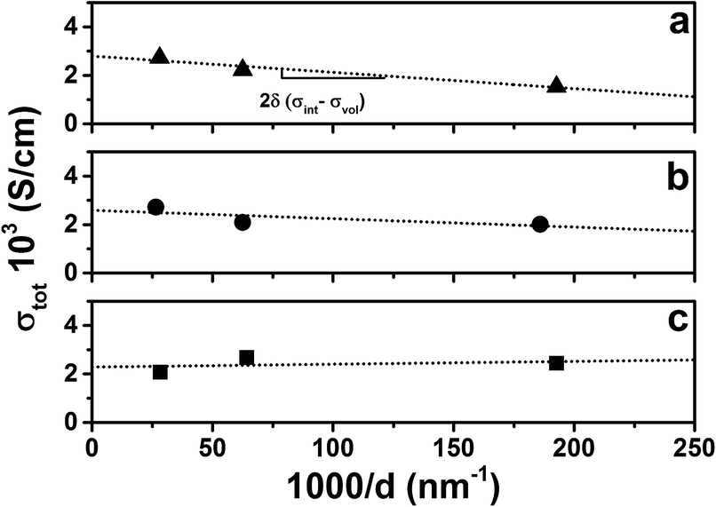 | ||
| Fig. 8 Conductivity isotherms at 650 °C of (a) YSZ/CeO2, (b) YSZ/CZO30, and (c) YSZ/CZO45 multilayers as a function of the reciprocal thickness of the YSZ layers, 1/d. | ||
Fig. 9 shows Arrhenius plots of the calculated volume or bulk and interfacial conductivities of the multilayers. The volume conductivities of each of the multilayers are highly similar to each other and to the total conductivity of the single-layer YSZ thin film. This result is intuitively expected, since the volume regions were thought to be unaffected by the interfaces. Fig. 9(a) compares the volume and interfacial conductivities in the YSZ/CeO2 multilayers. The interfacial conductivity is smaller by about a factor of ≈2. As mentioned before, this decreased conductivity may be due to interfacial roughness related to the very large lattice mismatch. As shown in Fig. 9(b) and (c), the volume and interfacial conductivities of the YSZ/CZO30 and YSZ/CZO45 multilayers are all nearly the same as the conductivity of a YSZ single-layer film. There is a correlation of increased interfacial conductivity as the zirconia content of the CZO layer is reduced (i.e., as the lattice mismatch with YSZ is reduced), though the changes are sufficiently small that this may be due to chance.
 | ||
| Fig. 9 The calculated volume (bulk) and interfacial conductivities for three different types of multilayers of (a) YSZ/CeO2, (b) YSZ/CZO30, and (c) YSZ/CZO45 as a function of temperature. The YSZ thin film data comes from measurements of a single layer film with thickness of ≈105 nm. | ||
In Korte et al.'s investigation of multilayers composed of YSZ and Y2O3, interfacial lattice mismatch of ≈+3% correlated to significant increases in conductivity.15 The total conductivity gradually increased by a factor of about 2 as the YSZ layer thickness decreased from 526 nm to 24 nm. At the same time, the activation energy decreased from 1.13 eV to 0.99 eV, suggesting that the strain was effectively increasing vacancy mobility. Li et al. studied multilayers composed of YSZ and Gd2Zr2O7, which has a similar lattice mismatch of +3% compared to the YSZ/Y2O3 multilayers.13 A key difference with this type of multilayers is that, unlike Y2O3, Gd2Zr2O7 is an oxygen ion conductor. There is thus the risk of a convolution of lattice mismatch strain-based effects, with the conducting phase on one side of the interface being compressed simultaneously with the conducting phase on the other side of the interface being expanded. Nevertheless, Li et al. reported that the +3% lattice mismatch caused the oxygen ion conductivity to increase by 2 orders of magnitude relative to bulk YSZ when the layer thickness decreased to 5 nm. The increased conductivity was attributed to the coherent, dislocation-free interfaces between YSZ and Gd2Zr2O7, imposing large tensile strain on YSZ layers.
In this work, we studied three different types of YSZ/CZO multilayers, but the tensile lattice mismatch caused very little effect on the oxygen ion transport properties. The XRD patterns shown in Fig. 2 indicate that the out-of-plane lattice parameters for YSZ were essentially unaffected across the range of lattice mismatch magnitudes and layer thicknesses employed in this study. The >+5% lattice mismatch between YSZ and pure CeO2 makes it likely that the strain was released by the creation of non-coherent interfaces in these multilayers. It is not surprising then that, as in ref. 19, no change in conductivity was measured.
The YSZ/CZO45 multilayers possess similar lattice mismatch as the YSZ/Y2O3 (ref. 15) and YSZ/Gd2Zr2O7 (ref. 13) multilayers. It is more surprising that no change in conductivity was measured in the YSZ/CZO45 multilayers, since the (ref. 13 and 15) suggest that YSZ was capable of accommodating this magnitude of lattice mismatch strain. Thus, we conclude that lattice mismatch strains of ≈+3% are close to a maximum practically achievable limit for YSZ, with the creation of coherent interfaces dependent on processing details. Continued research with high resolution transmission electron microscopy would enable visualization of the mechanism behind the strain relaxation. Based on the results discussed here, the insignificant effect of tensile lattice mismatch on the oxygen ion conductivity is due to strain relaxation even at “low” values of lattice mismatch and is not due to the lack of a mechano-electrochemical coupling effect. Reports of significantly greater tensile strains being accommodated in YSZ, therefore, must be treated with caution. Results from multilayers composed of doped ZrO2 and doped CeO2 that have been reported in the literature11,12 (e.g., YSZ and Ce0.8Sm2O2−δ) suggested that significant increase in conductivity can be derived due to >+5% lattice mismatch. It is difficult to believe that such large tensile strains could be accommodated in YSZ.
4. Conclusion
In this work, we studied the effects of tensile lattice mismatch on oxygen ion conductivity in multilayers composed of YSZ with CeO2, CZO30, and CZO45 with layer thicknesses ranging between 5 nm and 35 nm. Very little conductivity change was found in the multilayers, with values near that of bulk YSZ. Based on the calculated out-of-plane YSZ lattice parameters and the strong superlattice peaks in the diffraction patterns, it is believed that the lattice mismatch strain in the multilayers has been relaxed by the creation of incoherent interface structures. For YSZ/CZO45 multilayers, the lattice mismatch of +2.9%, is very similar as that of previously reported YSZ/Y2O3 multilayers, suggesting that biaxial strains of this magnitude represent a rough upper practical limit.Acknowledgements
Research supported by the U.S. Department of Energy, Office of Basic Energy Sciences, Division of Materials Sciences and Engineering under Award DE-SC0005403.References
- B. C. H. Steele and A. Heinzel, Nature, 2001, 414, 345–352 CrossRef CAS PubMed.
- Y. Arachi, H. Sakai, O. Yamamoto, Y. Takeda and N. Imanishai, Solid State Ionics, 1999, 121, 133–139 CrossRef CAS.
- F. M. L. Figueiredo and F. M. B. Marques, WIREs Energy Environ., 2013, 2, 52–72 CrossRef CAS.
- N. Q. Minh, J. Am. Ceram. Soc., 1993, 76, 563–588 CrossRef CAS PubMed.
- E. Fabbri, D. Pergolesi and E. Traversa, Sci. Technol. Adv. Mater., 2010, 11, 054503 CrossRef.
- J. Maier, Nat. Mater., 2005, 4, 805–815 CrossRef CAS.
- S. Ramanathan, J. Vac. Sci. Technol., A, 2009, 27, 1126–1134 CAS.
- X. X. Guo and J. Maier, Adv. Mater., 2009, 21, 2619–2631 CrossRef CAS.
- J. Garcia-Barriocanal, A. Rivera-Calzada, M. Varela, Z. Sefrioui, M. R. Diaz-Guillen, K. J. Moreno, J. A. Diaz-Guillen, E. Iborra, A. F. Fuentes, S. J. Pennycook, C. Leon and J. Santarnaria, ChemPhysChem, 2009, 10, 1003–1011 CrossRef CAS PubMed.
- X. Guo, Scr. Mater., 2011, 65, 96–101 CrossRef CAS PubMed.
- S. Azad, O. A. Marina, C. M. Wang, L. Saraf, V. Shutthanandan, D. E. McCready, A. El-Azab, J. E. Jaffe, M. H. Engelhard, C. H. F. Peden and S. Thevuthasan, Appl. Phys. Lett., 2005, 86, 131906 CrossRef PubMed.
- S. Sanna, V. Esposito, A. Tebano, S. Licoccia, E. Traversa and G. Balestrino, Small, 2010, 6, 1863–1867 CrossRef CAS PubMed.
- B. Li, J. M. Zhang, T. Kaspar, V. Shutthanandan, R. C. Ewing and J. Lian, Phys. Chem. Chem. Phys., 2013, 15, 1296–1301 RSC.
- W. D. Shen, J. Jiang, C. Y. Ni, Z. Voras, T. P. Beebe and J. L. Hertz, Solid State Ionics, 2014, 255, 13–20 CrossRef CAS PubMed.
- C. Korte, A. Peters, J. Janek, D. Hesse and N. Zakharov, Phys. Chem. Chem. Phys., 2008, 10, 4623–4635 RSC.
- C. Korte, N. Schichtel, D. Hesse and J. Janek, Monatsh. Chem., 2009, 140, 1069–1080 CrossRef CAS PubMed.
- N. Schichtel, C. Korte, D. Hesse and J. Janek, Phys. Chem. Chem. Phys., 2009, 11, 3043–3048 RSC.
- N. Schichtel, C. Korte, D. Hesse, N. Zakharov, B. Butz, D. Gerthsen and J. Janek, Phys. Chem. Chem. Phys., 2010, 12, 14596–14608 RSC.
- D. Pergolesi, E. Fabbri, S. N. Cook, V. Roddatis, E. Traversa and J. A. Kilner, ACS Nano, 2012, 6, 10524–10534 CAS.
- J. Garcia-Barriocanal, A. Rivera-Calzada, M. Varela, Z. Sefrioui, E. Iborra, C. Leon, S. J. Pennycook and J. Santamaria, Science, 2008, 321, 676–680 CrossRef CAS PubMed.
- X. Guo, Science, 2009, 324, 465 CrossRef CAS PubMed.
- J. Garcia-Barriocanal, A. Rivera-Calzada, M. Varela, Z. Sefrioui, E. Iborra, C. Leon, S. J. Pennycook and J. Santamaria, Science, 2009, 324, 465 CrossRef CAS.
- A. Cavallaro, M. Burriel, J. Roqueta, A. Apostolidis, A. Bernardi, A. Tarancon, R. Srinivasan, S. N. Cook, H. L. Fraser, J. A. Kilner, D. W. McComb and J. Santiso, Solid State Ionics, 2010, 181, 592–601 CrossRef CAS PubMed.
- C. E. Hori, H. Permana, K. Y. S. Ng, A. Brenner, K. More, K. M. Rahmoeller and D. Belton, Appl. Catal., B, 1998, 16, 105–117 CrossRef CAS.
- Y.-P. Fu, S.-H. Hu and B.-L. Liu, Ceram. Int., 2009, 35, 3005–3011 CrossRef CAS PubMed.
- M. Kuhn, S. R. Bishop, J. L. M. Rupp and H. L. Tuller, Acta Mater., 2013, 61, 4277–4288 CrossRef CAS PubMed.
- J. Jiang, W. D. Shen and J. L. Hertz, Thin Solid Films, 2012, 522, 66–70 CrossRef CAS PubMed.
- W. Shen, J. Jiang and J. L. Hertz, RSC Adv., 2014, 4, 21625–21630 RSC.
- S. Schweiger, M. Kubicek, F. Messerschmitt, C. Murer and J. L. M. Rupp, ACS Nano, 2014, 8, 5032–5048 CrossRef CAS PubMed.
- C. D. Wirkus, M. F. Berard and D. R. Wilder, J. Am. Ceram. Soc., 1969, 52, 456 CrossRef CAS PubMed.
- M. Boaro, A. Trovarelli, J. H. Hwang and T. O. Mason, Solid State Ionics, 2002, 147, 85–95 CrossRef CAS.
- G. R. Rao and H. R. Sahu, Proc.–Indian Acad. Sci., Chem. Sci., 2001, 113, 651–658 CrossRef CAS.
- H. Yamane and T. Hirai, J. Cryst. Growth, 1989, 94, 880–884 CrossRef CAS.
- M. O'Connell and M. A. Morris, Catal. Today, 2000, 59, 387–393 CrossRef.
- A. Atkinson and A. Selcuk, Solid State Ionics, 2000, 134, 59–66 CrossRef CAS.
- I. Kosacki, T. Suzuki, V. Petrovsky and H. U. Anderson, Solid State Ionics, 2000, 136, 1225–1233 CrossRef.
- T. Suzuki, I. Kosacki and H. U. Anderson, Solid State Ionics, 2002, 151, 111–121 CrossRef CAS.
- J. Jiang, X. Hu, W. Shen, C. Ni and J. L. Hertz, Appl. Phys. Lett., 2013, 102, 143901 CrossRef PubMed.
- I. Kosacki, T. Suzuki, V. Petrovsky and H. U. Anderson, Solid State Ionics, 2000, 136–137, 1225–1233 CrossRef CAS.
- V. Ruhrup and H. D. Wiemhofer, Z. Naturforsch., B: J. Chem. Sci., 2006, 61, 916–922 Search PubMed.
- A. Peters, C. Korte, D. Hesse, N. Zakharov and J. Janek, Solid State Ionics, 2007, 178, 67–76 CrossRef CAS PubMed.
| This journal is © The Royal Society of Chemistry 2015 |