 Open Access Article
Enhancement in the efficiency of an organic–inorganic hybrid solar cell with a doped P3HT hole-transporting layer on a void-free perovskite active layer†
Yunlong
Guo
,
Chao
Liu
,
Kento
Inoue
,
Koji
Harano
,
Hideyuki
Tanaka
* and
Eiichi
Nakamura
*
Department of Chemistry, The University of Tokyo, 7-3-1 Hongo, Bunkyo-ku, Tokyo 113-0033, Japan. E-mail: tanakah3@chem.s.u-tokyo.ac.jp; nakamura@chem.s.u-tokyo.ac.jp
First published on 20th June 2014
Abstract
Significant enhancement in the power conversion efficiency of an organic–inorganic hybrid solar cell was achieved by the use of suitably doped poly(3-hexylthiophene-2,5-diyl) (P3HT) spin coated on a 99.5% void-free perovskite layer prepared on a TiOx electron-transporting layer. The 9.2% device efficiency with pristine P3HT was increased to 12.4%.
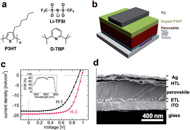
Solution-processable organic–inorganic hybrid solar cells utilizing a methylammonium lead halide perovskite (CH3NH3PbI3−xClx) semiconductor have quickly achieved a power conversion efficiency (PCE) as high as 15%.1–4 The high efficiency is due largely to high mobility of the perovskite (>10 cm2 V−1 s−1),5 and the long diffusion length for both holes and electrons in the perovskite layer.6,7 The uniformity of the perovskite layer and the efficiency of extracting free charge carriers through the electron- and hole-transporting layers (HTLs and ETLs) are two crucial factors to be optimized for further increase in the PCE.8–13 Poly(3-hexylthiophene-2,5-diyl) (P3HT, Fig. 1a), an inexpensive and readily available HTL material,14–16 has shown a PCE value of 10.8%,16 which is, however, not as satisfactory as those given by the use of structurally more elaborate HTL materials such as 2,2,7,7-tetrakis-(N,N-di-p-methoxyphenylamine)9,9-bifluorene (spiro-OMeTAD).12–14 We report here that an HTL composed of a ternary mixture of P3HT, an ionic dopant and a third additive, spin coated on a uniform and void-free (99.5% coverage) perovskite layer on indium tin oxide (ITO)/TiOx (Fig. 1b and d) brings about a considerable increase in the PCE value to 12.4% under the standard AM 1.5 conditions (Fig. 1c). This device shows an external quantum efficiency (EQE) of nearly 90% for a wide range of visible light (inset in Fig. 1c). The ionic dopant bis(trifluoromethane)sulfonimide lithium salt (Li-TFSI) was found to increase the carrier density in the HTL, while the third component, 2,6-di-tert-butylpyridine (D-TBP) (Fig. 1a) which was examined for the first time in this field research, was found to increase the mobility of the HTL as determined by mobility measurements, and as supported by the absorption spectra and X-ray diffraction (XRD) analysis that indicated enhanced ordering of the P3HT polymer chains. Such phenomena have not been reported in the previous study in the HTL doped with a popular additive, 4-tert-butylpyridine (TBP).15
The uniformity and crystallinity of the perovskite are crucial to achieving high efficiency in hybrid solar cells,16 and scanning electron microscopy (SEM) using a low landing voltage (1 kV) was found to provide a powerful tool for the analysis of the surface and the cross-section of organic and inorganic layers at ca. 1 nm resolution.17 A TiOx precursor solution was spin coated on a UV/ozone-treated ITO at 3000 rpm for 30 s and sintered at 500 °C for 30 min to form a flat ETL with a thickness of ca. 45 nm (Fig. 1d). This ETL is a uniform film made of nanoparticles of 15 to 20 -nm diameter (and see ESI, Fig. S1†). We then spin coated a 20 wt% solution of a mixture of CH3NH3I![[thin space (1/6-em)]](https://www.rsc.org/images/entities/char_2009.gif) :
:![[thin space (1/6-em)]](https://www.rsc.org/images/entities/char_2009.gif) PbCl2 in a 3
PbCl2 in a 3![[thin space (1/6-em)]](https://www.rsc.org/images/entities/char_2009.gif) :
:![[thin space (1/6-em)]](https://www.rsc.org/images/entities/char_2009.gif) 1 mole ratio in DMF at a slow spinning rate of 500 rpm for 60 s, and it was heated at 95 °C for 100 min, followed by rapid cooling to the room temperature under a nitrogen atmosphere. The crystalline perovskite active layer thus prepared was ca. 300 nm thick.
1 mole ratio in DMF at a slow spinning rate of 500 rpm for 60 s, and it was heated at 95 °C for 100 min, followed by rapid cooling to the room temperature under a nitrogen atmosphere. The crystalline perovskite active layer thus prepared was ca. 300 nm thick.
We noticed that the slow cooling tends to extend the void area, thus we adapted rapid cooling after the heating to prevent the void formation. The SEM and XRD analyses indicated that the rapidly cooled perovskite layer shows much better defined morphological and crystallographic properties than those reported previously.18
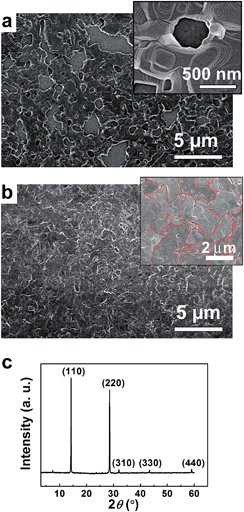
The cross-sectional view of the solar cell device formed on the rapidly cooled perovskite in Fig. 1d shows that the perovskite layer is very dense and uniform. The top view in Fig. 2b is representative of nine different areas of the rapidly cooled perovskite taken from three different samples, and indicates that 99.55 ± 0.24% of the surface is free of voids—a value significantly (see ESI, Fig. S2†) higher than the reported coverage of 95%.16 In contrast, the perovskite layer formed by slow cooling (Fig. 2a) exhibited a much larger void (i.e., an 82.2% void free region, see ESI, Fig. S3†), which might be caused by the formation of larger crystallites as observed in the clearly visible step and terrace structures (Fig. 2a inset). Although this subject is still under investigation, we could ascribe that the crystal growth during the cooling process might be the key for morphological control of the perovskite layer. The devices fabricated on the void-rich perovskite (i.e., 82.2% void-free) showed, not unexpectedly, only 6–8% PCE as opposed to the one made on a 99.5% void-free perovskite that showed 12.4% PCE.
The XRD pattern of the void-free perovskite film in Fig. 2c shows sharp and strong diffraction peaks at 14.19° and 28.48° due to the (110) and (220) crystal planes, and additional 31.88°, 43.33° and 58.7° peaks due to (310), (330) and (440) planes, respectively.9,16 Scherrer's analysis of the peaks19 gave a crystal grain size of ca. 1.5 μm, which agrees with the grain size of ca. 2 μm estimated from the top SEM view (Fig. 2b inset with red lines indicating grain boundaries). This crystal grain size is much larger than the reported sizes of ca. 0.5 μm.20
We next fabricated solar cell devices on the 99.5%-void-free perovskite layer, and examined the effects of doping of the P3HT-based HTL. The HTLs containing P3HT, Li-TFSI, and D-TBP as dopants in a variety of ratios are denoted as H-1 to H-4 as shown in Table 1 (see ESI, Fig. S4 and Table S1† for two additional HTLs H-5 and H-6 using Li-TFSI and D-TBP in different ratios). We chose the D-TBP additive rather serendipitously, knowing that it is a hindered base well-known in organic chemistry that can only react with proton without interaction with Lewis acidic metal atoms (e.g., Pb cation).
| HTL | P3HTa (mg) | Li-TFSIb (mg) | D-TBPc (mg) | J sc (mA cm−2) | V oc (V) | FF (%) | PCE (%) | R s (Ω cm2) | σ (S m−1) | HOMOd (eV) |
|---|---|---|---|---|---|---|---|---|---|---|
a P3HT dissolved in 1 mL of chlorobenzene.
b Li-TFSI dissolved in 6.8 μL of acetonitrile.
c 10.2 μL D-TBP was added to the P3HT![[thin space (1/6-em)]](https://www.rsc.org/images/entities/char_2009.gif) : :![[thin space (1/6-em)]](https://www.rsc.org/images/entities/char_2009.gif) Li-TFSI mixture solution.
d The HOMO level was estimated from photoelectron yield spectroscopy analysis. Li-TFSI mixture solution.
d The HOMO level was estimated from photoelectron yield spectroscopy analysis.
|
||||||||||
| H-1 | 15 | 0 | 0 | 17.7 | 0.92 | 56.2 | 9.2 | 12.4 | 5.4 × 10⁻⁴ | −4.70 |
| H-2 | 15 | 0.54 | 0 | 19.3 | 0.94 | 61.5 | 11.2 | 8.9 | 5.4 × 10⁻² | −4.79 |
| H-3 | 15 | 0.54 | 8.8 | 19.1 | 0.98 | 66.3 | 12.4 | 8.5 | 6.4 × 10⁻² | −4.80 |
| H-4 | 15 | 0 | 8.8 | 17.5 | 0.89 | 41.6 | 6.5 | 20.4 | 3.4 × 10⁻³ | −4.70 |
After spin coating at 2500 rpm for 30 s an HTL on the void-free perovskite followed by vacuum deposition of the Ag electrode, we examined the performance of the solar cells under simulated AM 1.5, 100 mW cm−2 irradiation (Fig. 1c). We summarize four representative results using H-1 to H-4 (Table 1). H-1 refers to pristine P3HT, H-2 to P3HT doped with Li-TFSI, H-3 to P3HT doped with Li-TFSI and D-TBP, and H-4 to P3HT doped only with D-TBP. The device coated with pristine P3HT (H-1) showed a PCE value of 9.2%, which is among the highest values reported for P3HT-based perovskite solar cells.16 The devices using H-2 showed a value of 11.2% and the device with H-3 showed a PCE of 12.4%, a 35% improvement over the 9.2% value for H-1. The short-circuit current density (JSC), open-circuit voltage (VOC) and fill-factor (FF) values are 19.1 mA cm−2, 0.98 V and 66.3%, respectively. A small dip around 600 nm in the EQE spectrum (Fig. 1c inset) is probably because of the absorption edge of the P3HT layer.21 The fabrication of the H-3 devices examined for 23 independent batches (see ESI, Fig. S6†) was found to be reproducible with the average PCE of 11.1% (±0.55%). In addition, the photocurrent density and the power conversion efficiency remained constant when applying 0.7 V voltage under the irradiation suggesting that our solar cell is stable under the operation conditions (see ESI, Fig. S6†).22
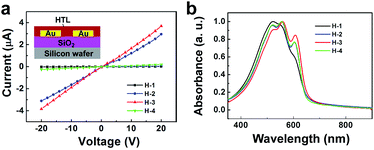
Upon addition of the Li-TFSI dopant to P3HT, JSC increased to a value of 19.3 mA cm−2, close to the saturation value.16 While Li-TFSI contributed to the slight increase in VOC and FF as well as in JSC, D-TBP contributed to a further increase in the former two without significant loss in JSC. The marked increase in FF is a direct consequence of the greatly decreased series resistance (RS) from 12.4 Ω cm2 for the H-1 cell to 8.9 Ω cm2 for the H-2 cell and 8.5 Ω cm2 for the H-3 cell, which is reflected in the 100-times larger conductivities in the two-terminal devices of the H-2 and H-3 thin films (σ = 5.4 × 10⁻² and 6.4 × 10⁻² S m−1, respectively) than that of the H-1 thin films (5.4 × 10⁻⁴ S m−1) (Table 1 and Fig. 3a).
While Li-TFSI increased the performance by increasing the carrier density, D-TBP may do so by increasing the mobility originating from the enhanced ordering of the P3HT polymer chains; that is, Fig. 3b shows the absorption spectra of H-1 to H-3 as well as H-4 (P3HT doped with D-TBP), where we see the appearance of increased peaks by addition of D-TBP (H-3 and H-4) at 561 nm and 610 nm with a concomitant decrease in the peak at 529 nm. This change in absorption is known to be the signature of enhanced ordering of P3HT in the solid state.23 Li-TFSI also enhances the ordering (H-2) and may cooperate with D-TBP. This conclusion was corroborated by XRD analysis and the field-effect mobility measurement. Thus, we saw first a marked enhancement of the 2θ peak at 5.25° that corresponds to a 1.68 nm d-spacing of the lamella layers, as well as at 23.5° corresponding to a 0.38 nm π–π interactive stacking distance,23 and also a four-times higher mobility of H-4 than H-1 (see ESI, Fig. S8†).
Photoelectron yield spectroscopy analysis of the HTLs (H-1 to H-4) indicated that the HOMO level decreases upon addition of Li-TFSI (from −4.70 eV for H-1 to −4.79 eV for H-2), but not upon addition of D-TBP (−4.70 eV for H-4) (see ESI, Fig. S9†). Thus Li-TFSI lowers the HOMO of the HTL closer to the valence band of the perovskite (−5.37 eV, see ESI Fig. S10†), which would help to increase the device performance.24
Conclusions
In summary, we have prepared an extremely homogeneous perovskite layer that is 99.5% free of voids, and fabricated an HTL based on the popular material P3HT. An ionic dopant Li-TFSI contributed to the increase in PCE by increasing the conductivity of the HTL, and a neutral additive D-TBP did so by enhancement of the ordering of the polymer chains of P3HT in the HTL. Thus, a ternary HTL, H-3, afforded 12.4% PCE—the highest PCE reported for the P3HT-based HTL in perovskite solar cells with its high reproducibility.Acknowledgements
We thank Dr Nai-Ti Lin for helpful discussion on perovskite precursor synthesis. We thank MEXT for the financial support [KAKENHI Specially Promoted Research Grant 22000008 to E.N., and Grant-in-Aid for Challenging Exploratory Research 26620203 to H.T.]. H.T. is supported by the Strategic Promotion of Innovative Research and Development from the Japan Science and Technology Agency.Notes and references
- G. Hodes, Science, 2013, 342, 317 CrossRef CAS PubMed.
- A. Kojima, K. Teshima, Y. Shirai and T. Miyasaka, J. Am. Chem. Soc., 2009, 131, 6050 CrossRef CAS PubMed.
- N.-G. Park, J. Phys. Chem. Lett., 2013, 4, 2423 CrossRef CAS.
- N. J. Jeon, J. Lee, J. H. Noh, M. K. Nazeeruddin, M. Grätzel and S. I. Seok, J. Am. Chem. Soc., 2013, 135, 19087 CrossRef CAS PubMed.
- C. Wehrenfennig, G. E. Eperon, M. B. Johnston, H. J. Snaith and L. M. Herz, Adv. Mater., 2014, 26, 1584 CrossRef CAS.
- G. C. Xing, N. Mathews, S. Y. Sun, S. S. Lim, Y. M. Lam, M. Grätzel, S. Mhaisalkar and T. C. Sum, Science, 2013, 342, 344 CrossRef CAS PubMed.
- S. D. Stranks, G. E. Eperon, G. Grancini, C. Menelaou, M. J. P. Alcocer, T. Leijtens, L. M. Herz, A. Petrozza and H. J. Snaith, Science, 2013, 342, 341 CrossRef CAS PubMed.
- J. You, Z. Hong, Y. Yang, Q. Chen, M. Cai, T.-B. Song, C.-C. Chen, S. Lu, Y. Liu, H. Zhou and Y. Yang, ACS Nano, 2014, 8, 1674 CrossRef CAS PubMed.
- P. W. Liang, C.-Y. Liao, C.-C. Chueh, F. Zuo, S. T. Williams, X.-K. Xin, J. J. Lin and A. K.-Y. Jen, Adv. Mater., 2014, 26, 3748 CrossRef CAS PubMed.
- M. Z. Liu, M. B. Johnston and H. J. Snaith, Nature, 2013, 501, 395 CrossRef CAS PubMed.
- J. Burschka, N. Pellet, S.-J. Moon, R. Humphry-Baker, P. Gao, M. K. Nazeeruddin and M. Grätzel, Nature, 2013, 499, 316 CrossRef CAS PubMed.
- D. Y. Liu and T. L. Kelly, Nat. Photonics, 2014, 8, 133 CrossRef CAS.
- J. H. Heo, S. H. Im, J. H. Noh, T. N. Mandal, C.-S. Lim, J. A. Chang, Y. H. Lee, H.-J. Kim, A. Sarkar, M. K. Nazeeruddin, M. Grätzel and S. I. Seok, Nat. Photonics, 2013, 7, 486 CrossRef CAS.
- O. Malinkiewicz, A. Yella, Y. H. Lee, G. M. Espallargas, M. Grätzel, M. K. Nazeeruddin and H. J. Bolink, Nat. Photonics, 2014, 8, 128 CrossRef CAS.
- F. Di Giacomo, S. Razza, F. Matteocci, A. D'Epifanio, S. Licoccia, T. M. Brown and A. D. Carlo, J. Power Sources, 2014, 251, 152 CrossRef CAS PubMed.
- B. Conings, L. Baeten, C. D. Dobbelaere, J. D'Haen, J. Manca and H.-G. Boyen, Adv. Mater., 2014, 26, 2041 CrossRef CAS PubMed.
- R. Young, S. Henstra, J. Chmelik, T. Dingle, A. Mangnus, G. van Veen and I. Gestmann, Proc. SPIE, 2009, 7378, 737803 CrossRef PubMed.
- G. E. Eperon, V. M. Burlakov, P. Docampo, A. Goriely and H. J. Snaith, Adv. Funct. Mater., 2014, 24, 151 CrossRef CAS.
- L. A. Patterson, Phys. Rev., 1939, 56, 978 CrossRef.
- J. M. Ball, M. M. Lee, A. Hey and H. J. Snaith, Energy Environ. Sci., 2013, 6, 1739 CAS.
- A. Abrusci, S. D. Stranks, P. Docampo, H.-L. Yip, A. K.-Y. Jen and H. J. Snaith, Nano Lett., 2013, 13, 3124 CrossRef CAS PubMed.
- H. J. Snaith, A. Abate, J. M. Ball, G. E. Eperon, T. Leijtens, N. K. Noel, S. D. Stranks, J. T.-W. Wang, K. Wojciechowski and W. Zhang, J. Phys. Chem. Lett., 2014, 5, 1511 CrossRef CAS.
- H. Sirringhaus, P. J. Brown, R. H. Friend, M. M. Nielsen, K. Bechgaard, B. M. W. Langeveld-Voss, A. J. H. Spiering, R. A. J. Janssen, E. W. Meijer, P. Herwig and D. M. de Leeuw, Nature, 1999, 401, 685 CrossRef CAS PubMed.
- P. Schulz, E. Edri, S. Kirmayer, G. Hodes, D. Cahen and A. Kahn, Energy Environ. Sci., 2014, 7, 1377 CAS.
Footnote |
| † Electronic supplementary information (ESI) available: Experimental details. See DOI: 10.1039/c4ta02976c |
| This journal is © The Royal Society of Chemistry 2014 |


