
 Open Access Article
 This Open Access Article is licensed under a Creative Commons Attribution-Non Commercial 3.0 Unported Licence
Effect of CH3NH3PbI3 thickness on device efficiency in planar heterojunction perovskite solar cells†
Dianyi
Liu
,
Mahesh K.
Gangishetty
and
Timothy L.
Kelly
*
Department of Chemistry, University of Saskatchewan, 110 Science Place, Saskatoon, SK, Canada. E-mail: tim.kelly@usask.ca; Fax: +1 306 966 4730; Tel: +1 306 966 4666
First published on 20th October 2014
Abstract
Recent advances in the development of perovskite solar cells based on CH3NH3PbI3 have produced devices with power conversion efficiencies of >15%. While initial work in this area assumed that the perovskite-based cells required a mesoporous TiO2 support, many recent reports have instead focused on the development of planar heterojunction structures. A better understanding of how both cell architecture and various design parameters (e.g., perovskite thickness and morphology) affect cell performance is needed. Here, we report the fabrication of perovskite solar cells based on a ZnO nanoparticle electron transport layer, CH3NH3PbI3 light absorber, and poly(3-hexylthiophene) (P3HT) hole transport layer. We show that vapor-phase deposition of the PbI2 precursor film produces devices with performances equivalent to those prepared using entirely solution-based techniques, but with very precise control over the thickness and morphology of the CH3NH3PbI3 layer. Optimization of the layer thickness yielded devices with efficiencies of up to 11.3%. The results further demonstrate that a delicate balance between light absorption and carrier transport is required in these planar heterojunction devices, with the thickest perovskite films producing only very low power conversion efficiencies.
1. Introduction
Perovskite-structured organometal halides (such as CH3NH3PbI3) have recently revolutionized the field of organic–inorganic hybrid solar cells.1–4 Their excellent optical and electronic properties, such as strong absorption bands that span the visible region5,6 and long charge carrier diffusion lengths,6–10 make them ideal light absorbers in photovoltaic devices. In the past 5 years, the power conversion efficiency (PCE) of perovskite solar cells has increased dramatically – from less than 4% in 2009 (ref. 11) to over 15% today,12–16 and estimates suggest that PCEs of over 20% are possible.3 Generally, these perovskite solar cells have been based on two different device architectures: (i) mesoscopic designs, and (ii) planar heterojunctions.2 Mesoscopic designs evolved from the traditional dye-sensitized solar cell (DSSC) structure, where the perovskite film is supported by an underlying mesoporous matrix of metal oxide nanoparticles. Since pioneering work by Kojima et al. in 2009,11 where cells based on CH3NH3PbI3 were shown to have PCEs of up to 3.8%, the performances of mesoscopic perovskite solar cells have improved rapidly. Optimization of the thickness of the mesoporous TiO2 layer and a post-annealing treatment improved PCEs to 6.5%,17 and the adoption of 2,2′,7,7′-tetrakis-(N,N-di-p-methoxyphenylamine)-9,9′-spiro-bifluorene (spiro-OMeTAD) as a solid-state hole transfer material pushed PCEs to nearly 10%.18 More recently, Snaith and coworkers demonstrated that charge injection into the mesoporous matrix is not a prerequisite for high power conversion efficiency; PCEs of >10% were obtained when the n-type TiO2 scaffold was replaced with an insulating Al2O3 analogue.19 While numerous other notable examples of mesoscopic perovskite solar cells have been reported,20–30 the most efficient devices (PCEs of ≥ 15%) were achieved when either a two-step deposition method was used to prepare the perovskite material inside the TiO2 matrix,12 or modified TiO2 layers were used as the electron selective contact.15,16While many of the perovskite solar cells reported to date have successfully adopted the mesoscopic design, the high temperatures associated with sintering a TiO2 mesoporous framework (>400 °C) have spurred the development of alternative cell architectures. Several examples of perovskite solar cells with a planar heterojunction structure have now been reported,14,31–37 with highly encouraging results. While initial reports of cells based on a CH3NH3PbI3/C60 planar heterojunction showed relatively modest efficiencies of 3.9%,31 organolead halide perovskite/fullerene heterojunctions have since achieved PCEs of up to 12%.32,33 Recently, vapor-phase deposition techniques have also been used to prepare perovskite solar cells with the structure ITO/TiO2/CH3NH3PbI3−xClx/spiro-OMeTAD/Ag, and displayed PCEs of up to 15.4%.13 Our recent work has also shown that planar heterojunction devices can be fabricated by the same two-step deposition procedure used by Burschka et al.,12 producing efficiencies of up to 15.7% on rigid substrates, and 10.2% on flexible supports.14 These devices are based on an ITO/ZnO/CH3NH3PbI3/spiro-OMeTAD/Ag structure, and are produced using solution-phase deposition techniques carried out at room temperature. The simplicity of the cell design and fabrication, when combined with their high performance and compatibility with flexible substrates, makes planar heterojunction perovskite solar cells a promising alternative to the original mesoscopic design.
One of the key variables in the fabrication of such devices is the thickness of the light harvesting perovskite layer. If the perovskite film is very thin, then the number of photons absorbed is low, resulting in low photocurrents; however, if very thick perovskite films are used, then the efficiency of charge carrier extraction is low, and recombination becomes problematic. Mesoscopic cells that use TiO2 photoanodes partially circumvent this issue by providing a large CH3NH3PbI3/TiO2 interfacial surface area; electrons are therefore extracted from the perovskite throughout the entire thickness of the light harvesting layer. Previous studies have shown that the PCE of devices of this type show a relatively weak dependence on perovskite layer thickness, with optimized photoanode thicknesses of ca. 650 nm.9 In planar heterojunction devices, the situation becomes more complex. Recent work has shown that film thicknesses of 400–800 nm can be used to successfully prepare high-performance devices based on CH3NH3PbI3−xClx in both conventional7,9,38 and inverted32 architectures. The very long charge carrier diffusion lengths observed for CH3NH3PbI3−xClx (ca. 1000 nm)7 mean that film thicknesses comparable to those of mesoscopic devices can be used. This is not the case for the parent CH3NH3PbI3 material, where the carrier diffusion lengths are an order of magnitude lower.7,8 Previous reports of planar heterojunction cells based on CH3NH3PbI3 have utilized perovskite layer thicknesses of only 100–350 nm,7,14,33–35 substantially thinner than those used in the chloride-doped analogues. Given the substantial differences in carrier diffusion lengths for these two perovskite compositions, a much deeper understanding of the role of film thickness and morphology on the efficiency of CH3NH3PbI3-based planar heterojunctions is required.
Here we report the fabrication of high performance perovskite (CH3NH3PbI3) solar cells with a planar heterojunction structure, and carefully elucidate the effect of perovskite film thickness and morphology on device efficiency. The perovskite films were deposited using a two-step deposition technique, with thermal evaporation used to prepare the PbI2 precursor film. This circumvents any issues with the solubility or viscosity of the PbI2 precursor solution, which have complicated these sorts of studies in the past. The evaporation of the PbI2 precursor allows perovskite films of precisely tailored thickness to be produced. Poly(3-hexylthiophene) (P3HT) was used as the hole transport material, and devices with the structure ITO/ZnO/CH3NH3PbI3/P3HT/Ag were prepared. Optimization of the film thickness produced power conversion efficiencies of up to 11.3%, which are among the highest ever reported for perovskite devices using a P3HT hole transport layer.
2. Experimental
2.1 Cell fabrication procedures
Solar cells were fabricated on pre-cleaned ITO-coated glass substrates with a sheet resistance of 20 Ω □−1. First, a thin ZnO nanoparticle layer was spin coated onto the substrate at 3000 rpm for 30 s. The procedure was repeated three times to obtain a continuous smooth film. Then a PbI2 layer of given thickness was deposited on top of the ZnO layer by thermal evaporation at a base pressure of 2 × 10⁻⁶ mbar. The final thickness was experimentally determined by profilometry. Subsequently, the substrate was dipped into a solution of CH3NH3I in 2-propanol (10 mg mL−1) for 3 min, then dried under a flow of clean air. For the solution PbI2-based device, a PbI2 solution (dissolved in N,N-dimethylformamide at a concentration of 460 mg mL−1) was then spin coated on top of the ZnO layer at 3000 rpm for 15 s. After drying for several minutes in air, the substrate was dipped into a solution of CH3NH3I in 2-propanol (10 mg mL−1) for 3 min. The P3HT-based hole transfer layer (20 mg of P3HT, 3.4 μL of 4-tert-butylpyridine, and 6.8 μL of a lithium–bis(trifluoromethanesulfonyl)imide (Li–TFSI) solution (28 mg Li-TFSI/1 mL acetonitrile) all dissolved in 1 mL chlorobenzene) was then deposited by spin coating at 1000 rpm for 30 s. Finally, a 150 nm thick silver layer was deposited by thermal evaporation at a base pressure of 2 × 10⁻⁶ mbar. The completed devices were stored in a N2-purged glovebox (<0.1 ppm O2 and H2O).2.2 Device characterization
The current–voltage curves of solar cells were measured inside the glovebox using a Keithley 2400 source-measure unit. The cells were illuminated by a 450 W Class AAA solar simulator equipped with an AM1.5G filter (Sol3A, Oriel Instruments) at a calibrated intensity of 100 mW cm−2, as determined by a standard silicon reference cell (91150V Oriel Instruments). The effective area of the cell was defined to be 0.07065 cm2 using a non-reflective metal mask. IPCE spectra were measured in air under short-circuit conditions using a commercial IPCE setup (QE-PV-Si, Oriel Instruments), which was equipped with a 300 W Xe arc lamp, filter wheel, and monochromator. Monochromated light was chopped at a frequency of 8 Hz and photocurrents measured using a lock-in amplifier. The setup was calibrated against a certified silicon reference diode. Electrochemical impedance spectroscopy (EIS) measurements were carried out using a Solartron SI1260 Impedance/Gain-phase analyzer, under 1 sun AM1.5G illumination, by applying 0 V DC bias and a 5 mV voltage perturbation in the frequency range of 400 kHz to 0.1 Hz.2.3 Thin film characterization
Film thicknesses were measured using a KLA Tencor profilometer. Absorption spectra were acquired on a Cary 6000i UV-vis-NIR spectrophotometer. Powder X-ray diffraction (pXRD) measurements were carried out using a PANalytical Empyrean X-ray diffractometer equipped with a Cu Kα1,2 X-ray source. The data were collected with a 0.02° step size (2θ). Scanning electron microscope (SEM) images were acquired on a JEOL 6010LV microscope. Atomic force microscope (AFM) images were acquired in contact mode on a Dimensions Hybrid Nanoscope system (Veeco Metrology Group).3. Results and discussion
3.1 Comparison of solution- and vapour-phase PbI2 deposition
The thin films of CH3NH3PbI3 used to fabricate the perovskite devices were prepared via the two-step deposition process described previously.12,14,39 As noted by Conings et al.,40 tailoring the thickness of perovskite films prepared via spin coating is complicated by the low solubility of the PbI2 precursor and the high viscosity of the precursor solution. We therefore used thermal evaporation39 to prepare thin films of PbI2 on ITO/ZnO substrates, rather than spin coating the PbI2 from DMF solution. The films were then dipped in an isopropanol solution of methylammonium iodide in order to convert the PbI2 to the organolead halide perovskite. The main advantage of this method is that the thickness of the PbI2 film (and therefore, the resultant perovskite layer) can be precisely controlled and systematically varied, without any complications due to the limited solubility of the precursor; additionally, the solvent-free method of PbI2 deposition may be useful in the future fabrication of tandem solar cells that include a perovskite component.Before the influence of perovskite layer thickness and morphology could be investigated, it needed to be determined whether the change in PbI2 deposition process would have any effect on the perovskite structure, morphology, or the performance of the resultant devices. As can be seen from the powder X-ray diffraction patterns of the PbI2 and CH3NH3PbI3 films (Fig. S1†), there are only minor differences in structure that arise as a result of the change in deposition process. Both PbI2 films are poorly crystalline (as evidenced by the weak, broad diffraction peaks), and data are consistent with the 2H polytype, in keeping with previous reports of solution-prepared PbI2 films.12 After dipping both samples in the CH3NH3I solution, both films are successfully converted into the corresponding perovskite. The diffraction patterns are consistent with the tetragonal phase of CH3NH3PbI3.41 The morphology of the perovskite films was also compared by SEM (Fig. S1†). Both films consisted of a closely-packed collection of block-like perovskite crystallites, with at most only very subtle differences in crystallite shape and size.
In order to gauge the effect of processing method on device efficiency, the perovskite films derived from both solution- and vapor-phase deposited PbI2 were used to prepare planar heterojunction solar cells. In both cases, the thickness of the perovskite film was determined to be ≈ 300 nm. A thin (ca. 30 nm) ZnO nanoparticle layer on ITO was chosen as the electron-selective contact, and P3HT was used as the hole transport material. The J–V curves of all devices were measured under AM1.5G illumination, and those of the highest-performing cells are shown in Fig. 1a. The results clearly indicate that the particular method of PbI2 deposition has little effect on the overall power conversion efficiency: the devices prepared using solution- and vapor-phase deposition techniques had PCEs of 11.8% and 11.3%, respectively. Both devices were also observed to have almost identical open-circuit voltages (Voc = 0.949 V and 0.941 V) and similar fill factors (FF = 66.1% and 68.2%). The only notable difference between the two devices was a slightly higher short-circuit current density for the solution-processed device (Jsc = 18.8 mA cm−2) compared to the one processed by thermal evaporation (Jsc = 17.6 mA cm−2). The lower Jsc in the device fabricated from vapor-deposited PbI2 is also reflected in the incident-photon-to-current efficiency (IPCE) spectrum (Fig. 1b). However, despite these small differences in Jsc, the difference in the overall PCE of devices constructed from both solution and vapor-deposited PbI2 is quite minor.
 | ||
| Fig. 1 (a) J–V curves and (b) IPCE spectra for the highest-performing ITO/ZnO/CH3NH3PbI3/P3HT/Ag devices prepared from both solution-processed (black line) and thermally evaporated (red line) PbI2 films. | ||
In order to ensure the reproducibility of our results, we fabricated and tested 34 separate devices using evaporated PbI2 layers, and 29 separate devices using spin coated PbI2 layers. The tabulated device performances are shown in Table 1. In this case, the average Jsc of the solution processed devices was found to be slightly higher (17.1 ± 1.1 mA cm−2) than that of the devices derived from evaporated PbI2 films (16.0 ± 0.9 mA cm−2), suggesting that the differences in Jsc observed in Fig. 1 simply reflect batch-to-batch variation in the perovskite layer, rather than any significant difference between the two fabrication processes. Similarly, the very small differences in Voc and FF (and ultimately, PCE) for the two fabrication methods are well within their associated standard deviations, indicating that the two methods produce cells of similar performance.
| PbI2 deposition method | V oc (V) | J sc (mA cm−2) | FF (%) | PCE (%) | Best PCE (%) |
|---|---|---|---|---|---|
| a Averages derived from measurements on 29 separate devices. b Averages derived from measurements on 34 separate devices. | |||||
| Spin coatinga | 0.94 ± 0.01 | 17 ± 1 | 62 ± 4 | 10.0 ± 0.9 | 11.8 |
| Thermal evaporationb | 0.94 ± 0.02 | 16.0 ± 0.9 | 65 ± 4 | 9.7 ± 0.6 | 11.3 |
3.2 Effect of PbI2 film thickness on CH3NH3PbI3 composition and morphology
Having established that the evaporated PbI2 films could be used to produce cells with power conversion efficiencies identical to those produced using solution-based techniques, we next investigated the effect of PbI2 film thickness on the composition, thickness, and morphology of the resultant perovskite layer. Lead iodide films were first deposited on glass substrates, and the thickness of the films was varied from 50 nm to 300 nm. The PbI2 films were then dipped in an isopropanol solution of methylammonium iodide in order to produce perovskite films of varying thickness. The thickness of the perovskite film was found to increase linearly with the thickness of the PbI2 precursor film, as shown in Fig. 2. Measurements were carried out on multiple films of each thickness, and the process was found to be highly reproducible, as indicated by the small standard deviations associated with the profilometry measurements. In all cases, the thickness of the perovskite film was found to be approximately twice that of the PbI2 precursor, in keeping with previous reports.34 More quantitatively, a linear regression of the data obtained for the three thinnest films yields a slope of 2.1. This can be understood based on the volume changes that occur during the intercalation of CH3NH3I into the PbI2 crystallites (Fig. S2†). The PbI2 that is initially present in the film has a unit cell volume of 124 Å3. Upon addition of CH3NH3I and formation of the perovskite structure, the unit cell volume increases dramatically to 990 Å3; however, since the tetragonal phase of the perovskite contains four CH3NH3PbI3 units within the unit cell, the molar volume of CH3NH3PbI3 is calculated to be 248 Å3. Comparing the molar volumes of PbI2 and CH3NH3PbI3, it can be seen that the volume occupied by the perovskite is almost exactly twice that of the PbI2 precursor, which is in excellent agreement with the data shown in Fig. 2a. However, for the thickest three films, the actual film thickness begins to deviate from that predicted by the above arguments. Upon measuring the powder X-ray diffraction patterns of perovskite films of various thicknesses, it can be seen that this is related to the presence of residual unreacted PbI2 in the film (Fig. 3). For the thinnest films, the diffraction patterns indicate complete conversion to the perovskite; however, beginning at ∼300 nm thick CH3NH3PbI3 films, there is evidence for the presence of residual PbI2. As the film thickness increases, the relative amount of unreacted PbI2 increases, in agreement with the data shown in Fig. 2a. | ||
| Fig. 2 (a) Perovskite film thickness as a function of the thickness of the precursor PbI2 film, as determined by profilometry; (b) absorbance spectra of the films from (a). Error bars represent plus-or-minus one standard deviation from the mean. | ||
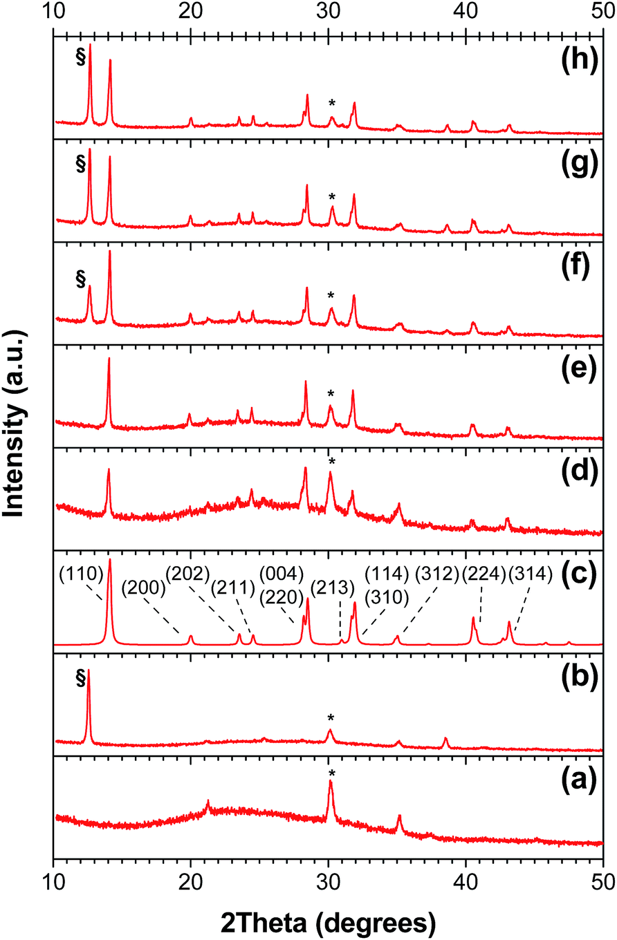 | ||
| Fig. 3 Powder X-ray diffraction patterns. All samples were prepared and measured on ITO/ZnO substrates. (a) Bare ITO/ZnO; (b) PbI2; (c) calculated diffraction pattern for the tetragonal phase of CH3NH3PbI3 (peak widths arbitrarily broadened to 0.2° 2θ). Where more than one reflection contributes to an unresolved peak, only the most intense reflection is labelled; (d) 61 nm CH3NH3PbI3; (e) 200 nm CH3NH3PbI3; (f) 280 nm CH3NH3PbI3; (g) 400 nm CH3NH3PbI3; (h) 560 nm CH3NH3PbI3. | ||
Fig. 2b shows the absorption spectra of the perovskite films as a function of film thickness. All perovskite films exhibited a broad range of light absorption from 300 to 760 nm, with the optical density of the film increasing monotonically with film thickness. The linear increase in optical density demonstrates both the excellent control over film thickness provided by the evaporation of PbI2, and the overall consistency of the two-step deposition process.
In order to understand how film thickness affects the morphology of the perovskite layer, both PbI2 and CH3NH3PbI3 films were evaluated by SEM (Fig. 4). Fig. 4a–c shows a top–down view of vapor-deposited PbI2 films of ca. 50, 150 and 300 nm thickness. The 50 nm thick film was relatively smooth, with only very small nanocrystallites visible under the electron microscope. As the film thickness is increased to 150 nm, the PbI2 crystallites begin to develop a flake-like texture, eventually becoming large nanoplates in the thickest films. After conversion to the perovskite (Fig. 4d–f), the morphology of the films is substantially altered; the film is still composed of a closely-packed collection of nanocrystallites, but the individual crystallites adopt a more block-like morphology, in keeping with the tetragonal perovskite unit cell. The same trend in morphology is also observed in the perovskite films. In the thinnest (ca. 110 nm) film, the block-like crystallites are small and densely packed, forming a film that, while not smooth, has very few gaps between the crystallites. As the perovskite film grows thicker, the individual nanocrystallites grow larger, in turn producing a rougher surface morphology. For the thickest (ca. 580 nm) film, many of the crystallites are over 100 nm in size, with equally large gaps between them; this produces a highly textured morphology.
 | ||
| Fig. 4 SEM images of (a–c) evaporated PbI2 films and (d–f) the corresponding CH3NH3PbI3 films after dipping in CH3NH3I. Films were (a) 50, (b) 150, (c) 300, (d) 110, (e) 330 and (f) 580 nm thick, as determined by profilometry. | ||
In order to more quantitatively evaluate these trends, we plotted both the particle size (as measured by SEM) and the minimum grain size (as determined from a Williamson–Hall analysis of the pXRD data, Fig. S3†) as a function of perovskite layer thickness (Fig. S4†). As suggested by Fig. 4, the average particle size increases as the perovskite layer is made thicker; however, this evolution in particle size is modest when compared to the pronounced morphological differences observed for the PbI2 films (Fig. 4). This suggests that a substantial degree of structural reorganization occurs within the crystallites during the CH3NH3I intercalation step, resulting in a highly crystalline perovskite film. This is supported by the Williamson–Hall analysis of the pXRD data, which separates out the effects of size and lattice strain on peak broadening (Fig. S3†). This analysis suggests that there is a slight dependence of the minimum grain size on the film thickness, with the thickest films having slightly larger crystalline domains than the thinnest samples. The degree of lattice strain is essentially negligible (<0.1%) for the majority of samples (Fig. S5†). Combined with the excellent agreement between the observed CH3NH3PbI3 thicknesses and those predicted based on the PbI2 precursor thickness and the subsequent increase in molar volume, this suggests that the Pb2+, I−, and CH3NH3+ ions are sufficiently mobile throughout the two-step deposition sequence to produce highly relaxed, crystalline films. This, in part, explains the excellent performance of the perovskite films fabricated using this technique.14,42 The one exception to this appears to be the thinnest films, which show a small amount of additional lattice strain, likely as a result of interactions with the underlying ZnO interface.
Since both the change in particle/grain size and the associated changes in surface roughness have important implications for device performance, we further probed the surface roughness of the samples using atomic force microscopy (Fig. S6†). The root-mean-square surface roughness (Rrms) of the perovskite films was found to change with increasing film thickness, with the thickest film (560 nm) showing a slightly higher Rrms (49 nm) compared to the rest of the samples (23–33 nm). The implications that this observation has for device performance are discussed in more detail below.
3.3 Device performance as a function of perovskite film thickness
A number of ITO/ZnO/CH3NH3PbI3/P3HT/Ag devices were fabricated at each of the perovskite thicknesses studied in Fig. 2a, and changes in device performance correlated with the observed changes in the optical density and morphology of the perovskite film. The J–V curves and IPCE spectra of the highest performing devices at each thickness are shown in Fig. 5, and Voc, Jsc, FF and PCE are plotted as a function of perovskite film thickness in Fig. 6. From the data, it is immediately apparent that device efficiency is strongly dependent on perovskite film thickness; both the thinnest and thickest perovskite films yield devices with PCEs of only 1–3%, while those with an optimal thickness of ca. 330 nm were found to have an average PCE of 9.4 ± 0.6%, with the best device displaying a PCE of 11.3%. Based on the data in Fig. 5 and 6, the improvements in PCE with increasing perovskite thickness are due to two dominant factors. The first is a dramatic increase in both Voc and FF as the thickness of the perovskite increases from 110 to 330 nm; based on the slopes of the corresponding J–V curves at Jsc, this is caused in large part by an increase in the shunt resistance (Table S1†). The low shunt resistances observed in the thinnest films are entirely consistent with substantial recombination at the ZnO interface, which leads to the pronounced loss in Voc. These losses are very similar to those observed in perovskite devices prepared via a one-step methodology,38 where pin-hole shorts lead to low shunt resistances and open-circuit voltages. Given that the Rrms in these films is ca. 30 nm (Fig. S6†), and that the Rrms represents only one standard deviation in the sample height, there is statistically a very high likelihood of pin-hole short formation in the thinnest perovskite films. Increasing the film thickness prevents such contact, resulting in improvements to both FF and Voc. These results are validated by electrochemical impedance spectroscopy measurements (Fig. 7); fitting the Nyquist plots to an equivalent circuit used for other solid-state photovoltaic devices43,44 shows that the thinnest devices have an extremely low recombination resistance (Table S2†). This is entirely consistent with the low fill factors observed in these devices, and provides an explanation for the losses observed in Voc. As the perovskite thickness is increased, the recombination resistance increases accordingly, which is consistent with the concomitant rise in FF and Voc. Very similar correlations have previously been observed between the recombination resistance and Voc in planar heterojunction perovskite solar cells.45 | ||
| Fig. 5 (a) J–V curves and (b) IPCE spectra for ITO/ZnO/CH3NH3PbI3/P3HT/Ag devices with perovskite layers of 110 (red line), 210 (orange line), 330 (yellow line), 410 (green line), 490 (blue line) and 580 nm (purple line). | ||
 | ||
| Fig. 6 (a) Open circuit voltage, (b) short circuit current density, (c) fill factor and (d) power conversion efficiency as a function of perovskite film thickness. Error bars represent plus-or-minus one standard deviation from the mean. Data are derived from measurements on 8, 17, 34, 12, 11 and 14 separate devices for 110, 210, 330, 410, 490, and 580 nm thick films, respectively. | ||
 | ||
| Fig. 7 Nyquist plots for ITO/ZnO/CH3NH3PbI3/P3HT/Ag devices with different CH3NH3PbI3 thicknesses: (a) 110 nm, (b) 330 nm, (c) 580 nm. Experimental data (black squares) and theoretical fit (red line). (d) Equivalent circuit model used to fit the data. | ||
The second factor leading to the observed increase in PCE is the steady increase in film optical density (Fig. 2b) with increasing thickness. For the thinnest films studied, the light harvesting efficiency at longer wavelengths is relatively low: at 700 nm, only ca. 69% of the incoming light is absorbed (assuming a 4% reflection loss at the air/glass interface, and 100% reflection at the silver back-contact), and when combined with high levels of recombination, this results in an IPCE of only ca. 40%. As the film thickness is increased, the light harvesting efficiency increases steadily; for the optimum film thickness of 330 nm, approximately 86% of the light at 700 nm is absorbed, leading to the stronger IPCE spectrum and improved Jsc. Since at this film thickness, only ca. 14% of the long wavelength light is lost to transmission, there is relatively little benefit to be realized from the use of thicker perovskite films.
For the devices with perovskite film thicknesses >400 nm, the decline in device performance is particularly sharp. As the film thickness continues to increase, there is a significant increase in the series resistance of the devices (Table S1†); the series resistance of the cells with the thickest perovskite layers is over an order of magnitude higher than for optimized devices. EIS measurements suggest that this is due to an increase in the contact resistance between the perovskite and interfacial layers (Table S2†); since the ZnO/CH3NH3PbI3 interface does not change as the perovskite thickness is increased, we ascribe this increase to changes in the CH3NH3PbI3/P3HT interface. This may suggest that for the thickest films, the polymer hole-transport material has difficulty penetrating into the porous surface; this would lead to an increased contact resistance, and contribute to the higher series resistance of these devices. Additionally, as the thickness is increased, there is also a drop in the shunt resistance (Table S1†). This may be related to the changing morphology of the perovskite layer; as the CH3NH3PbI3/P3HT interface becomes rougher (Fig. 4), there are also more opportunities for surface recombination to occur, and the efficiency is adversely impacted. Analogous behavior has been observed for perovskite solar cells with a high surface area ZnO/CH3NH3PbI3 interface.46 The combination of these two effects explains the observed drop in fill factor (64% to 42%).
Even more striking than the changes to the Voc and FF, however, is the dramatic loss (>75%) in Jsc as the perovskite film thickness begins to exceed 400 nm. This is by far the largest contributor to the reduced efficiency of the thickest devices, and is predominantly caused by the mismatch between the absorption depth of the perovskite and the carrier diffusion length. The electron and hole diffusion lengths for CH3NH3PbI3 have been reported to be ∼100 nm;7,8 however, for the thickest (580 nm) devices, the perovskite film thickness significantly exceeds the diffusion lengths of the charge carriers. As such, carriers generated near the center of the film will recombine before reaching the electrodes. This is consistent with the sharp decrease in IPCE observed for wavelengths > 500 nm (Fig. 5b). For wavelengths < 500 nm, the perovskite absorbs very strongly (Fig. 2b), and charge carriers are generated very close to the ZnO/CH3NH3PbI3 interface; as such, a reasonable number of electrons can be collected by the ZnO electron-transport layer before they recombine. For wavelengths > 500 nm, the lower extinction coefficient means that charge carriers are generated deep in the interior of the perovskite film and are more than 100 nm away from either interface. As such, the carrier collection efficiency in this spectral region begins to approach zero, resulting in the very low short-circuit current densities that are observed. Additionally, the less-compact perovskite morphology observed in thicker films (Fig. 4f) may result in poorer connectivity between adjacent crystallites, leading to a more tortuous pathway for carrier transport and a greater likelihood of recombination. Given the observed decrease in PCE, the increased light harvesting efficiency observed in the thicker films (96% at 700 nm for the thickest film, vs. 86% for the optimum thickness of 330 nm) is clearly insufficient to overcome these deleterious effects on carrier transport. This same argument would also hold true (although to a lesser degree) for the optimized perovskite film thickness of 330 nm. A large number of carriers would be generated in the innermost 130 nm of the perovskite film; since these are greater than an exciton diffusion length away from the electron- and hole-transport interfaces, many of these would be expected to recombine. However, given the good IPCE values achieved in these devices, this is clearly not the case. There are two possible explanations for this observation: (i) the carrier diffusion lengths are significantly longer than those originally reported by Stranks et al. and Xing et al.;7,8 or, (ii) carrier extraction is facilitated by the high surface area CH3NH3PbI3/P3HT interface. Although the measurements of Stranks et al. and Xing et al.7,8 are fairly conservative estimates, we believe that the high surface area CH3NH3PbI3/P3HT interface plays a key role in the high performance of these planar heterojunction devices. This can be understood more quantitatively by considering the highest performance devices, which have a 330 nm thick perovskite layer. The first 130 nm of this film is within one charge carrier diffusion length of the ZnO interface,7 and carrier collection is not expected to be problematic. Similarly, holes can readily be extracted from the 110 nm closest to the P3HT interface.7 This leaves ca. 90 nm in the interior of the film that is too far away from either interface to meaningfully contribute to the photocurrent. However, AFM measurements indicate that the CH3NH3PbI3/P3HT interface has a Rrms of 20–30 nm. Again, considering that the Rrms value represents the standard deviation of the sample height, the maximum peak-to-trough variation in the perovskite interface is closer to 60–90 nm. As a result, charge carriers can be extracted from much deeper within the perovskite film than would be the case if the CH3NH3PbI3/P3HT interface were completely planar (Fig. S7†). Although there is still a very small section of the perovskite film that still does not contribute to the overall photocurrent in this model (<30 nm), the discrepancy is quite small, and likely due to slightly longer charge carrier diffusion lengths in our films.
Hysteresis in the J–V curve is now a well-known issue for perovskite solar cells,47 and it results in a differential current response depending on the history of applied bias. In order to show that the trends observed in Fig. 6 are the result of changes in film thickness (and not due to changes in hysteretic behaviour), we measured the J–V curves using both forward (short-circuit to forward-bias) and reverse (forward-bias to short-circuit) scans for a series of representative devices (Fig. 8). As with many planar heterojunction devices, the hysteresis is quite pronounced, with the reverse scan having a substantially higher efficiency (Fig. 8a). However, the magnitude of the hysteresis was found to depend only very weakly on the thickness of the perovskite film (Fig. 8b). This suggests that batch-to-batch variability in sample preparation has as much or more influence over the hysteresis than the film thickness. Therefore, while these results suggest that the absolute efficiencies of these devices are lower than might be expected from measurements of just the reverse scan, the overall trends in device performance (Fig. 6) are actually due to changes in film thickness, and not due to changes in hysteretic behaviour.
 | ||
| Fig. 8 (a) J–V curves for a representative ITO/ZnO/CH3NH3PbI3/P3HT/Ag device, measured from forward-bias (FB) to short-circuit (SC), and from short-circuit to forward-bias. (b) Ratio of the power conversion efficiencies measured from FB to SC and from SC to FB as a function of perovskite film thickness. Measurements were the average of at least 6 devices, and the error bars represent plus or minus one standard deviation from the mean. | ||
4. Conclusions
In summary, we have demonstrated that the thermal evaporation of PbI2 films, in combination with a CH3NH3I treatment, is a highly reproducible method of preparing planar heterojunction devices with very precise control over the perovskite film thickness. The optical properties and morphology of the perovskite films were measured as a function of film thickness, and the results correlated with changes in device performance. The improved light harvesting efficiency and reduced contact between electron- and hole-transport layers was found to improve the power conversion efficiency and increase the recombination resistance for thicker films; however, once the film thickness significantly exceeded the carrier diffusion lengths in CH3NH3PbI3, the efficiency declined sharply. At the optimum thickness of 330 nm, ITO/ZnO/CH3NH3PbI3/P3HT/Ag devices were found to have power conversion efficiencies of up to 11.3% when fabricated from evaporated PbI2 layers, and 11.8% when prepared from solution-processed analogues; these efficiencies are among the highest reported for devices that use a P3HT hole-transport layer. It is expected that by better understanding the parameters that govern the efficiency of CH3NH3PbI3-based planar heterojunction devices, further improvements in device performance can be realized.Acknowledgements
The Natural Sciences and Engineering Research Council of Canada (NSERC) and the University of Saskatchewan are acknowledged for financial support. T.L.K. is a Canada Research Chair in Photovoltaics. The research was undertaken, in part, thanks to funding from the Canada Research Chair program. Mr John Hayes and Ms Esther Aluri are gratefully acknowledged for their assistance with the pXRD measurements. Mr Robert Peace is gratefully acknowledged for his assistance with the SEM measurements.Notes and references
- S. Kazim, M. K. Nazeeruddin, M. Grätzel and S. Ahmad, Angew. Chem., Int. Ed., 2014, 53, 2812–2824 CrossRef CAS PubMed.
- H. J. Snaith, J. Phys. Chem. Lett., 2013, 4, 3623–3630 CrossRef CAS.
- N.-G. Park, J. Phys. Chem. Lett., 2013, 4, 2423–2429 CrossRef CAS.
- P. Gao, M. Grätzel and M. K. Nazeeruddin, Energy Environ. Sci., 2014, 7, 2448–2463 CAS.
- D. B. Mitzi, in Progress in Inorganic Chemistry, John Wiley & Sons, Inc., 2007, pp. 1–121 Search PubMed.
- T. C. Sum and N. Mathews, Energy Environ. Sci., 2014, 7, 2518–2534 CAS.
- S. D. Stranks, G. E. Eperon, G. Grancini, C. Menelaou, M. J. P. Alcocer, T. Leijtens, L. M. Herz, A. Petrozza and H. J. Snaith, Science, 2013, 342, 341–344 CrossRef CAS PubMed.
- G. Xing, N. Mathews, S. Sun, S. S. Lim, Y. M. Lam, M. Grätzel, S. Mhaisalkar and T. C. Sum, Science, 2013, 342, 344–347 CrossRef CAS PubMed.
- Y. Zhao and K. Zhu, J. Phys. Chem. Lett., 2013, 4, 2880–2884 CrossRef CAS.
- C. Wehrenfennig, G. E. Eperon, M. B. Johnston, H. J. Snaith and L. M. Herz, Adv. Mater., 2014, 26, 1584–1589 CrossRef CAS.
- A. Kojima, K. Teshima, Y. Shirai and T. Miyasaka, J. Am. Chem. Soc., 2009, 131, 6050–6051 CrossRef CAS PubMed.
- J. Burschka, N. Pellet, S.-J. Moon, R. Humphry-Baker, P. Gao, M. K. Nazeeruddin and M. Grätzel, Nature, 2013, 499, 316–319 CrossRef CAS PubMed.
- M. Liu, M. B. Johnston and H. J. Snaith, Nature, 2013, 501, 395–398 CrossRef CAS PubMed.
- D. Liu and T. L. Kelly, Nat. Photonics, 2014, 8, 133–138 CrossRef CAS.
- J. T.-W. Wang, J. M. Ball, E. M. Barea, A. Abate, J. A. Alexander-Webber, J. Huang, M. Saliba, I. Mora-Sero, J. Bisquert, H. J. Snaith and R. J. Nicholas, Nano Lett., 2013, 14, 724–730 CrossRef PubMed.
- K. Wojciechowski, M. Saliba, T. Leijtens, A. Abate and H. J. Snaith, Energy Environ. Sci., 2014, 7, 1142–1147 CAS.
- J.-H. Im, C.-R. Lee, J.-W. Lee, S.-W. Park and N.-G. Park, Nanoscale, 2011, 3, 4088–4093 RSC.
- H.-S. Kim, C.-R. Lee, J.-H. Im, K.-B. Lee, T. Moehl, A. Marchioro, S.-J. Moon, R. Humphry-Baker, J.-H. Yum, J. E. Moser, M. Grätzel and N.-G. Park, Sci. Rep., 2012, 2, 591 Search PubMed.
- M. M. Lee, J. Teuscher, T. Miyasaka, T. N. Murakami and H. J. Snaith, Science, 2012, 338, 643–647 CrossRef CAS PubMed.
- Z. Ku, Y. Rong, M. Xu, T. Liu and H. Han, Sci. Rep., 2013, 3, 3132 Search PubMed.
- W. A. Laban and L. Etgar, Energy Environ. Sci., 2013, 6, 3249–3253 CAS.
- J. Shi, J. Dong, S. Lv, Y. Xu, L. Zhu, J. Xiao, X. Xu, H. Wu, D. Li, Y. Luo and Q. Meng, Appl. Phys. Lett., 2014, 104, 063901 CrossRef PubMed.
- D. Bi, S.-J. Moon, L. Haggman, G. Boschloo, L. Yang, E. M. J. Johansson, M. K. Nazeeruddin, M. Grätzel and A. Hagfeldt, RSC Adv., 2013, 3, 18762–18766 RSC.
- J. H. Heo, S. H. Im, J. H. Noh, T. N. Mandal, C.-S. Lim, J. A. Chang, Y. H. Lee, H.-j. Kim, A. Sarkar, M. K. Nazeeruddin, M. Grätzel and S. I. Seok, Nat. Photonics, 2013, 7, 486–491 CrossRef CAS.
- J. H. Noh, S. H. Im, J. H. Heo, T. N. Mandal and S. I. Seok, Nano Lett., 2013, 13, 1764–1769 CAS.
- J. M. Ball, M. M. Lee, A. Hey and H. J. Snaith, Energy Environ. Sci., 2013, 6, 1739–1743 CAS.
- B. Cai, Y. Xing, Z. Yang, W.-H. Zhang and J. Qiu, Energy Environ. Sci., 2013, 6, 1480–1485 CAS.
- E. Edri, S. Kirmayer, D. Cahen and G. Hodes, J. Phys. Chem. Lett., 2013, 4, 897–902 CrossRef CAS.
- N. Pellet, P. Gao, G. Gregori, T.-Y. Yang, M. K. Nazeeruddin, J. Maier and M. Grätzel, Angew. Chem., Int. Ed., 2014, 53, 3151–3157 CrossRef CAS PubMed.
- Y. Ogomi, A. Morita, S. Tsukamoto, T. Saitho, N. Fujikawa, Q. Shen, T. Toyoda, K. Yoshino, S. S. Pandey, T. Ma and S. Hayase, J. Phys. Chem. Lett., 2014, 5, 1004–1011 CrossRef CAS.
- J.-Y. Jeng, Y.-F. Chiang, M.-H. Lee, S.-R. Peng, T.-F. Guo, P. Chen and T.-C. Wen, Adv. Mater., 2013, 25, 3727–3732 CrossRef CAS PubMed.
- P. Docampo, J. M. Ball, M. Darwich, G. E. Eperon and H. J. Snaith, Nat. Commun., 2013, 4, 2761 Search PubMed.
- O. Malinkiewicz, A. Yella, Y. H. Lee, G. M. Espallargas, M. Grätzel, M. K. Nazeeruddin and H. J. Bolink, Nat. Photonics, 2014, 8, 128–132 CrossRef CAS.
- Q. Chen, H. Zhou, Z. Hong, S. Luo, H.-S. Duan, H.-H. Wang, Y. Liu, G. Li and Y. Yang, J. Am. Chem. Soc., 2013, 136, 622–625 CrossRef PubMed.
- S. Sun, T. Salim, N. Mathews, M. Duchamp, C. Boothroyd, G. Xing, T. C. Sum and Y. M. Lam, Energy Environ. Sci., 2014, 7, 399–407 CAS.
- A. Yella, L.-P. Heiniger, P. Gao, M. K. Nazeeruddin and M. Grätzel, Nano Lett., 2014, 14, 2591–2596 CrossRef CAS PubMed.
- C. Roldan-Carmona, O. Malinkiewicz, A. Soriano, G. Minguez Espallargas, A. Garcia, P. Reinecke, T. Kroyer, M. I. Dar, M. K. Nazeeruddin and H. J. Bolink, Energy Environ. Sci., 2014, 7, 994–997 CAS.
- G. E. Eperon, V. M. Burlakov, P. Docampo, A. Goriely and H. J. Snaith, Adv. Funct. Mater., 2014, 24, 151–157 CrossRef CAS.
- K. Liang, D. B. Mitzi and M. T. Prikas, Chem. Mater., 1998, 10, 403–411 CrossRef CAS.
- B. Conings, L. Baeten, C. De Dobbelaere, J. D'Haen, J. Manca and H.-G. Boyen, Adv. Mater., 2014, 26, 2041–2046 CrossRef CAS PubMed.
- T. Baikie, Y. Fang, J. M. Kadro, M. Schreyer, F. Wei, S. G. Mhaisalkar, M. Grätzel and T. J. White, J. Mater. Chem. A, 2013, 1, 5628–5641 CAS.
- J. Burschka, N. Pellet, S. J. Moon, R. Humphry-Baker, P. Gao, M. K. Nazeeruddin and M. Grätzel, Nature, 2013, 499, 316–319 CrossRef CAS PubMed.
- P. P. Boix, Y. H. Lee, F. Fabregat-Santiago, S. H. Im, I. Mora-Sero, J. Bisquert and S. I. Seok, ACS Nano, 2011, 6, 873–880 CrossRef PubMed.
- I. Mora-Seró, J. Bisquert, F. Fabregat-Santiago, G. Garcia-Belmonte, G. Zoppi, K. Durose, Y. Proskuryakov, I. Oja, A. Belaidi, T. Dittrich, R. Tena-Zaera, A. Katty, C. Lévy-Clément, V. Barrioz and S. J. C. Irvine, Nano Lett., 2006, 6, 640–650 CrossRef PubMed.
- S. Chavhan, O. Miguel, H.-J. Grande, V. Gonzalez-Pedro, R. S. Sanchez, E. M. Barea, I. Mora-Sero and R. Tena-Zaera, J. Mater. Chem. A, 2014, 2, 12754–12760 CAS.
- M. H. Kumar, N. Yantara, S. Dharani, M. Grätzel, S. Mhaisalkar, P. P. Boix and N. Mathews, Chem. Commun., 2013, 49, 11089–11091 RSC.
- H. J. Snaith, A. Abate, J. M. Ball, G. E. Eperon, T. Leijtens, N. K. Noel, S. D. Stranks, J. T.-W. Wang, K. Wojciechowski and W. Zhang, J. Phys. Chem. Lett., 2014, 5, 1511–1515 CrossRef CAS.
Footnote |
| † Electronic supplementary information (ESI) available: Powder X-ray diffraction patterns, SEM and AFM images, Williamson–Hall plots, crystallite size and strain data, tabulated resistance data and impedance parameters. See DOI: 10.1039/c4ta02637c |
| This journal is © The Royal Society of Chemistry 2014 |