 Open Access Article
 This Open Access Article is licensed under a
 Creative Commons Attribution 3.0 Unported Licence
Air-stable high-efficiency solar cells with dry-transferred single-walled carbon nanotube films†
Kehang
Cui
a,
Anton S.
Anisimov
b,
Takaaki
Chiba
a,
Shunjiro
Fujii
c,
Hiromichi
Kataura
c,
Albert G.
Nasibulin
de,
Shohei
Chiashi
a,
Esko I.
Kauppinen
d and
Shigeo
Maruyama
*a
aDepartment of Mechanical Engineering, The University of Tokyo, Bunkyo-ku, Tokyo 113-8656, Japan. E-mail: maruyama@photon.t.u-tokyo.ac.jp; Fax: +81-3-5800-6983; Tel: +81-3-5841-6421
bCanatu Ltd, Konalankuja 5, FI-00390 Helsinki, Finland
cNanosystem Research Institute, National Institute of Advanced Industrial Science and Technology, Tsukuba 305-8562, Japan
dDepartment of Applied Physics, Aalto University School of Science, Aalto FI-00076, Finland
eSkolkovo Institute of Science and Technology, 100 Novaya st., Skolkovo, Moscow Region, Russia 143025
First published on 23rd April 2014
Abstract
By using the excellent optical and electrical properties of pristine SWNTs with long bundle lengths, we present single-walled carbon nanotube–silicon (SWNT/Si) solar cells of 11% power conversion efficiency (PCE), prepared without doping. The PCEs of the fabricated solar cells even increased slightly after 10 months of exposure to ambient conditions, without any external protection. The open-circuit voltage of the SWNT/Si solar cells under low light intensities, down to 10 mW cm−2, demonstrated the characteristics of the ideal p–n junction model. The mechanism was discussed, taking into account the effect of varying the interfacial oxide layer thickness between the SWNTs and Si on the solar cell’s performance. The high efficiency and stability demonstrated in this study make SWNT/Si solar cells one of practical choices for next generation energy system.
Introduction
Single-walled carbon nanotubes (SWNTs) possess excellent optical,1 electrical,2 mechanical and thermal properties,3as well as chemical stability. Specifically, for light harvesting applications, SWNTs are superior in terms of their wide spectrum of absorption ranging from the near-infrared to visible wavelengths, their high electrical conductivity and transparency,4 as well as their multiple exciton generation properties.5 Combining these properties with their earth abundance and chemical stability, SWNTs are considered to be a very promising candidates for next-generation solar cell applications.6,7Recently, SWNT/Si solar cells have attracted increasing attention, owing to their simple and efficient structures.8–18 The power conversion efficiencies (PCEs) of SWNT/Si solar cells have been improved by an order of magnitude over the last five years. However, the so-far-reported peak PCEs of SWNT/Si solar cells have all been negatively affected by degradation, which hinders the further applications of the cells. The SWNT/Si solar cells could lose almost 50% of their PCE after hours in air and, even with protection, the PCE was still degraded by 20%.10–14 This could be attributed to the fact that the peak PCEs had been boosted by doping with nitric acid or gold salt, which were very unstable. Another issue that has remained controversial is the working mechanism of the SWNT/Si solar cells. Initially, the SWNT/Si solar cell was proposed to form a p–n heterojunction by Jia et al.8,9 Based on this hypothesis, (6,5) enriched SWNTs were used19 to further increase the built-in potential. However, the incident photon conversion efficiency (IPCE) spectrum of the SWNT/Si solar cells showed no obvious relationship to the SWNT absorption spectrum. In addition, the efficiency of the graphene–Si solar cell20,21 became comparable to that of the SWNT/Si solar cell. The SWNT/Si solar cells were considered to form Schottky-barrier junctions. One characteristic that could distinguish the p–n junction and the Schottky-barrier junction is the effect of the interfacial oxide layer. For a conventional Schottky-barrier junction, inserting an interfacial oxide layer between the metal electrode and semiconductor would eliminate the pinning of the Fermi level and thus improve the PCE, while the opposite case applies for a p–n junction. Until now, both a significant improvement22 and degradation12 of the PCEs have been obtained after the removal of the interfacial oxide layer. These contradictory results call for more solid experimental proof for the further understanding of the SWNT/Si solar cells.
In this work, we utilize pristine SWNTs with long bundle lengths for the fabrication of SWNT/Si solar cells. The record-high PCE approaching 11% is achieved for the solar cell sample using a pristine SWNT film without any chemical treatment. More importantly, the peak PCE is stable for at least 10 months in air with no external protection. In fact, a slight increase in the PCE value was observed, rather than the severe decreases reported in previous literature. The operation mechanism of the SWNT/Si solar cell is discussed based on this highly efficient system.
Materials and experiments
The randomly oriented SWNT films with high purity and long nanotube bundle lengths were synthesized by an aerosol CVD method.23,24 The floating catalyst aerosol CVD was carried out in a scaled-up reaction tube with a diameter of 150 mm. Ferrocene vapor was thermally decomposed in the gas phase in the aerosol CVD reactor at a temperature of 880 °C. The CO gas was supplied at 4 L min−1 and decomposed on the iron nanoparticles, which resulted in the growth of the SWNTs. The floating catalysts have three-dimensional freedom which leads to the long bundle lengths. The as-synthesized SWNTs were collected by passing the flow through microporous filters downstream of the reactor. The transparency of the SWNT films was controlled by changing the collection time. The collected SWNT films could be transferred to arbitrary substrates using the dry transfer method, a sonication- and surfactant-free process that could retain the excellent properties of the SWNTs.Each SWNT/Si solar cell was fabricated by dry-transferring the SWNT film onto a designed substrate, which was composed of a 3 mm × 3 mm n-type Si contact window and surrounding electrodes. The n-type Si (SUMCO Inc.) has a series resistance of 10 ± 2.5 Ω cm−1 with a dopant concentration of ∼1015 m−3. The fabrication process of the Si substrate for the SWNT/Si solar cell is given in Fig. 1a. Before the metal deposition, the n-type Si substrate was sequentially treated with RCA1 (H2O![[thin space (1/6-em)]](https://www.rsc.org/images/entities/char_2009.gif) :NH4OH:H2O2 = 5:1:1), 5 M NaOH and RCA2 (H2O:HCl:H2O2 = 5:1:1) solution for 10 min, 40 min and 5 s, respectively, for the removal of organic contaminants, oxide layers and metal impurities. After the cleaning treatment, a very thin oxide layer with a thickness of 6 Å–7 Å was formed, according to the Si 2p spectrum measured by X-ray photoelectron spectroscopy (XPS, PHI 5000 VersaProbe) (see detailed discussion in the ESI: S1†). 3 mm × 3 mm physical masks were patterned on the top surfaces of the Si substrates before the metal deposition. A 200 nm-thick SiO2 insulator layer and a 50 nm-thick Pt electrode were subsequently RF-sputtered (ULVAC-RIKO, Inc.) onto the top surface of the Si substrate. Ti with a thickness of 10 nm was selected as the back electrode for the lineup of the band structure. The SWNT films were transferred using a dry-transfer method onto the top surface of the Si substrate after the removal of the physical masks. The schematic of the fabricated SWNT/Si solar cell with dimensional parameters is shown in Fig. 1b. Part of the SWNT film with a width of 300 nm was suspended between the Pt electrode and the Si substrate (Fig. 1c), owing to the stair-shape formed by the SiO2 insulator and the Pt electrode layers. The size of the suspended region can be ignored, in comparison with that of the SWNT/Si contact window.
:NH4OH:H2O2 = 5:1:1), 5 M NaOH and RCA2 (H2O:HCl:H2O2 = 5:1:1) solution for 10 min, 40 min and 5 s, respectively, for the removal of organic contaminants, oxide layers and metal impurities. After the cleaning treatment, a very thin oxide layer with a thickness of 6 Å–7 Å was formed, according to the Si 2p spectrum measured by X-ray photoelectron spectroscopy (XPS, PHI 5000 VersaProbe) (see detailed discussion in the ESI: S1†). 3 mm × 3 mm physical masks were patterned on the top surfaces of the Si substrates before the metal deposition. A 200 nm-thick SiO2 insulator layer and a 50 nm-thick Pt electrode were subsequently RF-sputtered (ULVAC-RIKO, Inc.) onto the top surface of the Si substrate. Ti with a thickness of 10 nm was selected as the back electrode for the lineup of the band structure. The SWNT films were transferred using a dry-transfer method onto the top surface of the Si substrate after the removal of the physical masks. The schematic of the fabricated SWNT/Si solar cell with dimensional parameters is shown in Fig. 1b. Part of the SWNT film with a width of 300 nm was suspended between the Pt electrode and the Si substrate (Fig. 1c), owing to the stair-shape formed by the SiO2 insulator and the Pt electrode layers. The size of the suspended region can be ignored, in comparison with that of the SWNT/Si contact window.
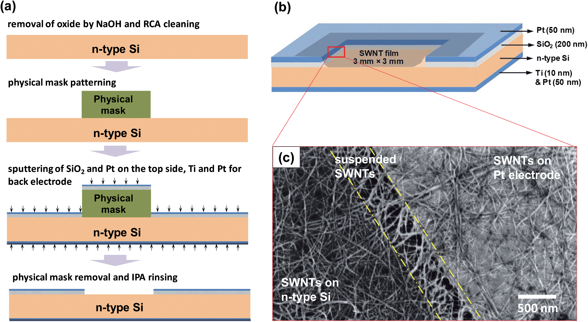 | ||
| Fig. 1 (a) Fabrication process of the n-type Si substrate for the SWNT/Si solar cell. (b) Schematic of the SWNT/Si solar cell with dimensional parameters. (c) Magnified SEM image of the contact window edge of the SWNT/Si solar cell. A region of the SWNT film with a width of 300 nm was suspended between the Si substrate and the Pt electrode. | ||
Results and discussion
Electrical and optical characterization of the SWNTs
The as-synthesized SWNT films collected on the filter were subsequently dry-transferred to fused quartz substrates and densified by drop-casting approximately 20 μL of ethanol and drying in an ambient environment. From the optical image shown in Fig. 2a, it can be observed that the SWNT film is highly transparent and uniform. The SEM (Hitachi S-4800) images of the corresponding SWNT films at low and high magnifications are shown in Fig. 2b. The SWNT films are well percolated, with predominantly Y-junction inter-tube contact, which would facilitate the carrier transport between the SWNTs.25 As opposed to the films prepared by the filtration method, the SWNTs used in this study have very long bundle lengths, averaging 9.4 μm.24 The Raman spectra were measured on a thicker SWNT film to obtain stronger signals. As shown by the Raman spectra (Renishaw inVia) in Fig. 2c, the SWNT films have very high crystallinity, with G/D ratios over 30. The radial breathing modes (RBMs) of the Raman spectra under the excitation laser wavelengths of 488, 532, 633 and 785 nm are also shown in Fig. 2c. The peak RBM intensity positions are located at ca. 120 cm−1 to 130 cm−1 for all the laser excitation wavelengths, thus the mean diameter of the SWNTs is estimated26 as 2.0–2.1 nm. The mean diameter is further confirmed by the E11 position (∼2400 nm) from the transmittance spectrum in Fig. 2d. Because no surfactant was used, nor was a sonication process involved during film preparation, the high crystallinities, good inter-tube contact and very long bundle lengths of the SWNTs are well retained. This leads to the high optical transparency and electrical conductivity of the SWNT films, as well as the simultaneous good contact with other materials. The sheet resistances (Agilent 4156C; Kyowa-Riken K89PS) and the transmittances (Shimadzu UV-3150) measured at a wavelength of 550 nm (550 nm is the wavelength that has the highest spectral irradiance in the AM1.5G spectrum shown in Fig. 2d) for all of the pristine SWNT films are listed in Table 1. The TCF samples with transmittances of around 70%, 80% and 90% are labelled as TCF70, TCF80 and TCF90, respectively. The sheet resistance was measured by a four-point probe method, and calculated by averaging the values measured from −0.5 V to 0.5 V with a measurement step of 5 mV. Table 1 shows that, among the randomly oriented pristine SWNT films reported so far,4,27,28 the SWNT films used in this study possess the best transparency and conductivity, with very high SWNT crystallinity.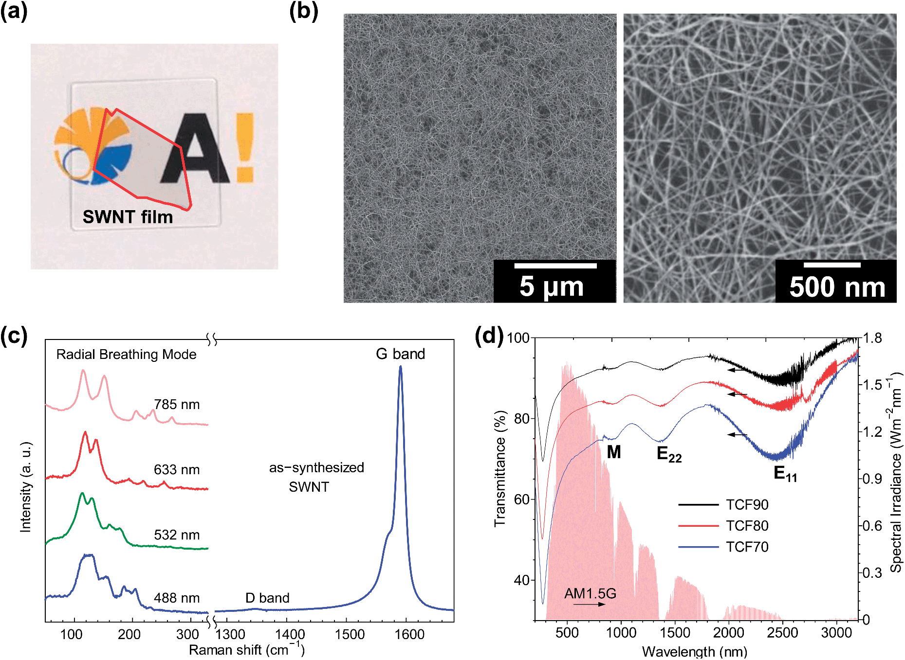 | ||
| Fig. 2 (a) An SWNT film on the fused quartz substrate after the dry-transfer process. (b) The SEM images at low and high magnifications of the SWNT film from (a). (c) Raman spectra of the SWNT film under laser excitation with the wavelengths of 488 nm, 532 nm, 633 nm and 785 nm. (d) Transmission spectra of the TCF70, TCF80 and TCF90 SWNT films over the wavelength range of 200 nm to 3200 nm, with an AM1.5G irradiance spectrum. | ||
| SWNT films | Transmittance (%) | Sheet resistance (Ω sq−1) |
|---|---|---|
| TCF70 | 70.0 | 85 |
| TCF80 | 81.5 | 134 |
| TCF90 | 88.8 | 417 |
J–V characteristics of SWNT/Si solar cells
The current density–voltage (J–V) characteristics of the SWNT/Si solar cells using the TCF70, TCF80 and TCF90 films were measured under AM1.5G 100 mW cm−2 illumination (PEC-L01, Peccell Technologies, Inc.) as shown in Fig. 3a. The obtained peak PCE values for the solar cells with the TCF70, TCF80 and TCF90 SWNT films are 9.2%, 10.8% and 10.1%, respectively. The PCE of the solar cell using the TCF80 film is the highest among the pristine SWNT/Si solar cells reported so far, and is comparable to that of the SWNT/Si solar cells doped with nitric acid and/or gold salt in the previous literature.8–12 The superiority of this PCE over those in the previous reports is attributed to the well-retained high crystallinity and long tube lengths of the SWNTs, as well as the sound inter-SWNT and SWNT–Si contact. The open-circuit photovoltage (Voc), short-circuit photocurrent (Jsc), fill factor (FF) and PCE values of the fabricated solar cells are listed in Table 2. The Jsc values of the solar cell samples with the TCF70, TCF80 and TCF90 films were 25.7, 29.7 and 30.9 mA cm−2, respectively. The calculated value of Jsc from the integration of the spectral responsivity (see the ESI S5†) with the AM1.5G irradiance spectrum is 30.3 mA cm−2, which was calibrated by the reference Si p–n solar cell samples. The record high PCE of the pristine SWNT/Si solar cells is attributed to the very long lengths of the SWNT bundles. Theoretically, higher transmittance would allow more solar irradiation to reach the SWNT/Si interface, hence the higher photocurrent. However, the photocurrents of the fabricated solar cells do not vary linearly with the transparency of the SWNT films. This could be attributed to a lesser contribution by the SWNTs, owing to the decreased light absorbance of the SWNTs. In addition, the energy loss from the light reflection by the mirror-like Si surface becomes notable, and increases with the increase in the transparency of the SWNT film.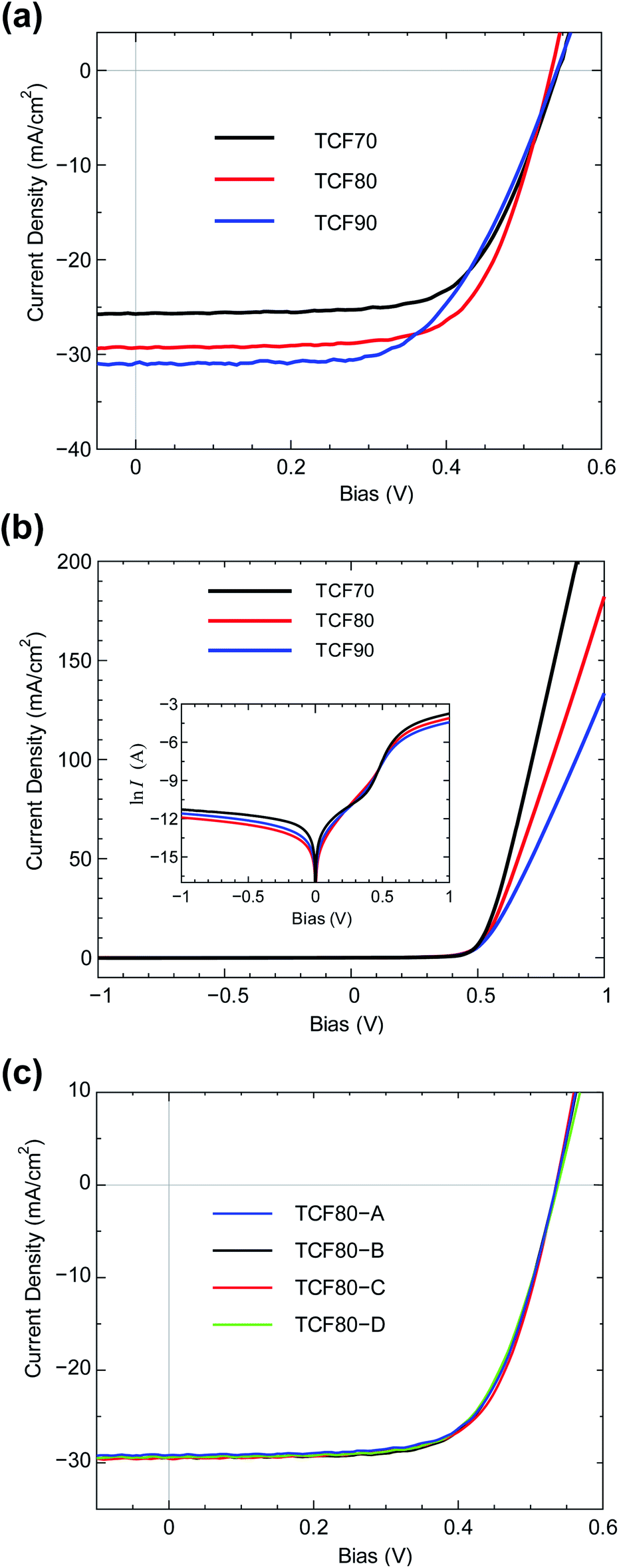 | ||
| Fig. 3 (a) Representative J–V characteristics of the SWNT/Si solar cells with the TCF70, TCF80 and TCF90 films under 100 mW cm−2 AM1.5 G illumination. (b) J–V characteristics of the SWNT/Si solar cells under dark conditions. (c) Reproducibility of the J–V characteristics of four solar cell samples with the TCF80 films fabricated in the same batch. | ||
| Films | Experimental results | Modeling results | |||||||
|---|---|---|---|---|---|---|---|---|---|
| Time of measurement | PCE (%) | FF (−) | J sc (mA cm−2) | V oc (mV) | R S (Ω) | R SH (kΩ) | I 0 (pA) | ||
| TCF70 | Immediately | 9.3 | 0.68 | 25.7 | 535 | 27.5 | >20 | 635 | |
| TCF80 | A | 10.6 | 0.68 | 29.3 | 535 | — | — | — | |
| B | 10.7 | 0.67 | 29.6 | 535 | — | — | — | ||
| C | 10.8 | 0.68 | 29.7 | 535 | 27.5 | >20 | 144 | ||
| D | 10.6 | 0.67 | 29.6 | 535 | — | — | — | ||
| TCF90 | 10.1 | 0.61 | 30.9 | 535 | 33.8 | >20 | 847 | ||
| 10 months | 10.2 | 0.62 | 30.3 | 549 | — | — | — | ||
The J–V characteristics of the SWNT/Si solar cells under dark conditions are shown in Fig. 3b. The rectification ratio of 1 V to −1 V is more than ∼2 × 10³, which demonstrates the excellent diode behavior of the SWNT/Si junction. The ideality factors are calculated as the slopes of the J–V curves on a logarithmic scale (inset of Fig. 3b) ranging from 0.4 V to 0.6 V, which are 1.7, 2.1 and 2.2 for the solar cells using the TCF70, TCF80 and TCF90 films, respectively. Moreover, in order to test the reproducibility of the fabricated solar cells, four solar cell samples using the TCF80 films, i.e., TCF80-A, TCF80-B, TCF80-C and TCF80-D, were compared, as shown in Fig. 3c. The uncertainties of the Voc, Jsc, FF and PCE are within 2.5 mV, 0.2 mA cm−2, 0.005 and 0.15%, respectively, demonstrating the high reproducibility of the solar cell’s performance. The four above-mentioned solar cell samples used for the comparison are from the same batch. The experimental fluctuations among samples from different batches of fabrication are also very small, as discussed in the ESI S2.† The high reproducibility of the fabricated SWNT/Si solar cells makes their use in practical applications possible.
Record-high stability
Besides the PCE value, the stability is an important factor in evaluating a newly emerging solar cell. In this research, we rendered the outstanding chemical stability of the pristine SWNTs, for the realization of a steady and highly efficient output for solar cells without any external protection. After the fabrication of the SWNT/Si solar cells was complete, the solar cell samples were stored in a well-ventilated lab. As shown in Fig. 4a, the J–V characteristics underwent almost no change over the ten-month duration under ambient conditions. Actually, the Voc values increased by 13 mV to 550 mV (Fig. 4b). This can be attributed to the modification of the SWNT films by oxygen, which would p-dope the SWNTs29 and shift the Fermi level downwards. This would further enlarge the built-in voltage, leading to the increase of Voc. The charge transfer and Fermi level change of the SWNTs was confirmed by the blue shift of the G band in the Raman spectrum (see the ESI S3†). In previous literature, the Voc value of 550 mV could only be achieved by strong and versatile oxidizing agents, e.g. nitric acid, hydrogen peroxide, etc., the doping effect of which lasts for only a few hours. In our study, the mild and stable doping effect from the ambient environment upon the SWNT films is very suitable for practical applications. This is the only stable over-10%-PCE SWNT/Si solar cell reported so far. The high-quality pristine SWNTs used in the present study are inherently much more stable than those obtained by sealing techniques such as PDMS coating. Moreover, the PCE of the SWNT/Si solar cells could possibly be further increased by roughly 30% by applying a TiO2 antireflection layer.13,15 It is worth mentioning that no external techniques, such as chemical doping or an antireflection layer, have been employed so far. We believe that a stable or even higher peak PCE would be achieved by applying the TiO2 coating technique to the current SWNT/Si solar cells.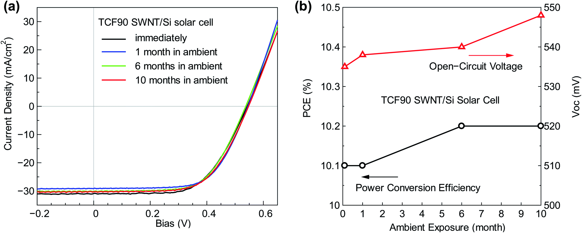 | ||
| Fig. 4 (a) J–V characteristics of the SWNT/Si solar cell using the TCF90 film, when measured immediately, as well as after 1, 6 and 10 months of exposure to ambient conditions. (b) The changes in the PCE and Voc of the SWNT/Si solar cell using the TCF90 film over 10 months of exposure to ambient conditions. | ||
Light intensities: experiments and modeling
In practical applications, the light intensity varies by many factors and is usually lower than the 100 mW cm−2 used in standard solar tests. The decrease in the light intensity would result in decreases of Jsc and Voc. The Jsc varies in proportion to the light intensity and thus will not actually affect the PCE. However, the degradation of Voc resulting from the decrease in the light intensity will reduce the PCE.30 Therefore, the Voc of the solar cell under a light intensity of lower than 100 mW cm−2 is another important parameter characterizing the quality of the solar cell. In this research, the dependency of the Voc of the SWNT/Si solar cells using the TCF90 films on the light intensity was examined. As shown in Fig. 5a, the Voc experienced only a 10% drop from 540 to 460 mV (the measurement uncertainty was 2.5 mV) when the light intensity decreased from 100 to 10 mW cm−2. Fig. 5b shows the J–V characteristics of the SWNT/Si solar cell using the TCF90 film measured under the illuminations of 100, 78, 50 and 20 mW cm−2. The PCE value of the solar cell only decreased slightly with the decrease in the light intensity, making it suitable for applications in low light intensities.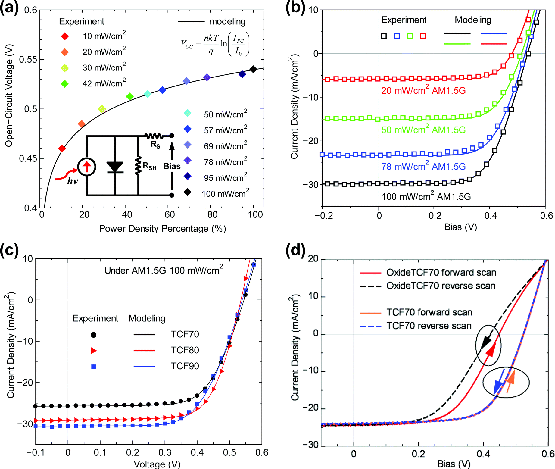 | ||
| Fig. 5 (a) The dependency of the open-circuit voltage on light intensity. The line is the modeling result of this dependency. The inset is the equivalent circuit of the SWNT/Si solar cells. (b) J–V characteristics of the SWNT/Si solar cells in different light intensities. The symbols denote the experimental results, while the lines represent the modeling results obtained by the p–n diode equation. (c) The curve fitting of the J–V characteristics of the SWNT/Si solar cells using the TCF70, TCF80 and TCF90 films. (d) Hysteresis of the forward and reverse scans for the OxideTCF70 and TCF70 samples which respectively have oxide layers with thicknesses of around 15 Å and 7 Å between the SWNT films and Si substrates. | ||
The curve fitting of the experimental J–V characteristics of the solar cells is an insightful method for the in-depth investigation of the solar cells’ performances. In this research, the equivalent circuit shown in the inset of Fig. 5a was used to model the J–V characteristics of the SWNT/Si solar cells. The corresponding p–n diode equation is expressed as
 | (1) |
 | (2) |
 | (3) |
As shown in Fig. 5a, the experimental dependency of Voc on the light intensity can fit the ideal Voc model well, which demonstrates that the RSH of the solar cell is large enough for the light intensities ranging from 100 to 10 mW cm−2. Therefore, the SWNT/Si solar cells in this study operate soundly under low light intensities.
To further investigate the effects of RS and RSH, the equivalent circuit model was also used to fit the J–V curves of the fabricated SWNT/Si solar cells measured under different light intensities, with the aim of extracting the RS and RSH. As shown in Fig. 5b, the J–V curves of the SWNT/Si solar cell using the TCF90 film under different light intensities all fit the p–n diode solar cell model of eqn (1) well. The obtained RS and RSH of the solar cell using the TCF90 film were calculated as 33.8 Ω and more than 20 kΩ, respectively. The curve fitting results of the J–V characteristics of the SWNT/Si solar cells with the TCF70 and TCF80 films are also shown in Fig. 5c. The calculated RS for the SWNT/Si solar cells using the TCF70 and TCF80 films have the same value of 27.5 Ω. The obtained RSH for these two solar cell samples were also more than 20 kΩ. The obtained RS, RSH and I0 for the SWNT/Si solar cells using the TCF70, TCF80 and TCF90 films are listed in Table 2.
The RS and RSH determine the quality of a solar cell, i.e., FF, which is one of the three parameters characterizing solar cell performance, along with Jsc and Voc. The FF values for the SWNT/Si solar cells using the TCF70, TCF80 and TCF90 films were 68%, 68% and 61%, respectively. As discussed above, the effect of RSH on the performance of the solar cells is ignorable. The RS is composed of four factors, i.e., the SWNT film–electrode contact, the sheet resistance of the SWNT film, the resistance of the Si substrate, and the resistance of the electrode. Except for the sheet resistance of the SWNT film, the three factors are inherent and can be considered to be the same in one fabrication batch. As the TCF90 has the highest sheet resistance among all the films, the solar cell using the TCF90 film has a lower FF. However, whilst the SWNT/Si solar cells with the TCF70 and TCF80 films have the same RS and FF, the sheet resistance of the TCF70 film is lower than that of the TCF80 film. This suggests that when the sheet resistance of the SWNT film is as low as 100 Ω sq−1, the inherent resistance of the solar cell architecture becomes dominant. The FFs of all of the solar cell samples using the randomly oriented films in this study were limited to 68%. Previously, we have reported a record-high FF of up to 72% using microhoneycomb-networked SWNTs,17 in which the micro-grids made of dense SWNT walls significantly reduced the carrier diffusion length from millimeter-scale to micrometer-scale. It is expected that applying a specially-designed three-dimensional structure to the SWNT films could further increase the FFs.
Interfacial oxide layers
We further investigated the effect of the interfacial oxide layers on the performances of the SWNT/Si solar cells. For Schottky-barrier Si solar cells, it has been well studied that inserting an oxide layer with a thickness of 13–20 Å between the metal and semiconductor would improve a solar cell’s performance by eliminating the pinning of the Fermi level.32–34 This theory was used to partially explain the substantial increase of the peak PCE by adding nitric acid or other strong oxidants to the SWNT/Si solar cells which were then considered as Schottky-barrier solar cells. In this study, we designed an experiment to verify this hypothesis. The TCF70 SWNT films were used to fabricate two kinds of SWNT/Si solar cells with different interfacial oxide layer thicknesses, as the TCF70 SWNT film possesses the highest electrical conductivity among all of the TCF films used in this research, and could best simulate the metal part in a Schottky solar cell. Two Si substrates with different oxide layer thicknesses were prepared by varying the treatment time of the RCA2 cleaning. The Si substrate treated by the RCA2 solution for 5 s was utilized for the fabrication of the TCF70 solar cell sample which has the above-mentioned performance (Fig. 3a and b), while the Si substrate treated for 3 min was used for the fabrication of the OxideTCF70 solar cell sample (dashed curves in Fig. 5d). According to the Si 2p XPS spectrum (ESI† S5), the oxide thickness of the Si substrate for the TCF70 solar cell sample was calculated as 6.9 Å which was approximately the limit of the native oxide layer grown in air.35–37 In the case of the Si substrate for the OxideTCF70 solar cell sample, the 3 min RCA2 cleaning would leave an oxide layer with a thickness of 13–15 Å, which has been thoroughly investigated in the previous literature.38,39 As shown in Fig. 5d, the PCE, FF and Voc of the OxideTCF70 solar cell sample were significantly lower than those of the TCF70 solar cell sample. The photocurrent degradation near the Voc is attributed to the increase in the series resistance between the SWNT film and Si substrate. Moreover, in the case of the OxideTCF70 solar cell, the thick oxide layer between the SWNT film and the Si substrate serves as a dielectric capacitor. The hysteresis between the forward and reverse scans of the OxideTCF70 solar cell sample results from the charging and discharging of the dielectric layer. This experimental result serves as indirect evidence of the insufficiency of the MIS mechanism for the SWNT/Si solar cells fabricated in this research. The SWNT/Si solar cell is different from the conventional metal–insulator–semiconductor (MIS) junction.Conclusions
We have demonstrated air-stable SWNT/Si solar cells with PCEs approaching 11% for the first time. The PCE of the solar cell slightly increases after 10 months of exposure to ambient conditions. Compared with previously reported results, the fabricated solar cells show significantly higher stability. The experimental results fit the p–n diode equation model well and the mechanisms of the improved performances of the SWNT/Si solar cells are discussed accordingly. We believe that the full exploitation of the superior electrical, optical and chemical properties of SWNTs is very promising for the next generation of photovoltaic devices.Acknowledgements
Part of this work was financially supported by JSPS Grant-in-Aid for Scientific Research (22226006, 23760180, 23760179, 25630063, 25107002, 25220602), Aalto Energy Efficiency (AEF) program via the MOPPI project and from Canatu Ltd., JST-EC DG RTD Coordinated Research Project ‘IRENA’ within the Strategic International Collaborative Research Program (SICORP), and Takuetsu Program ‘GMSI’ by the Ministry of Education, Culture, Sport, Science and Technology, Japan.Notes and references
- P. Avouris, M. Freitag and V. Perebeinos, Nat. Photonics, 2008, 2, 341–350 CrossRef CAS.
- D. Jariwala, V. K. Sangwan, L. J. Lauhon, T. J. Marks and M. C. Hersam, Chem. Soc. Rev., 2013, 42, 2824–2860 RSC.
- M. Marconnet, M. A. Panzer and K. E. Goodson, Rev. Mod. Phys., 2013, 85, 1295–1326 CrossRef.
- Z. Wu, Z. Chen, X. Du, J. M. Logan, J. Sippel, M. Nikolou, K. Kamaras, J. R. Reynolds, D. B. Tanner, A. F. Hebard and A. G. Rinzler, Science, 2004, 305, 1273–1276 CrossRef CAS PubMed.
- N. M. Gabor, Acc. Chem. Res., 2013, 46, 1348–1357 CrossRef CAS PubMed.
- R. H. Baughman, A. A. Zakhidov and W. A. de Heer, Science, 2002, 297, 787–792 CrossRef CAS PubMed.
- M. F. L. De Volder, S. H. Tawfick, R. H. Baughman and A. J. Hart, Science, 2013, 339, 535–539 CrossRef CAS PubMed.
- J. Wei, Y. Jia, Q. Shu, Z. Gu, K. Wang, D. Zhuang, G. Zhang, Z. Wang, J. Luo, A. Cao and D. Wu, Nano Lett., 2007, 7, 2317–2321 CrossRef CAS PubMed.
- Y. Jia, J. Wei, K. Wang, A. Cao, Q. Shu, X. Gui, Y. Zhu, D. Zhuang, G. Zhang, B. Ma, L. Wang, W. Liu, Z. Wang, J. Luo and D. Wu, Adv. Mater., 2008, 20, 4594–4598 CrossRef CAS.
- Y. Jia, P. Li, X. Gui, J. Wei, K. Wang, H. Zhu, D. Wu, L. Zhang, A. Cao and Y. Xu, Appl. Phys. Lett., 2011, 98, 133115 CrossRef PubMed.
- Y. Jia, A. Cao, X. Bai, Z. Li, L. Zhang, N. Guo, J. Wei, K. Wang, H. Zhu, D. Wu and P. M. Ajayan, Nano Lett., 2011, 11, 1901–1905 CrossRef CAS PubMed.
- Y. Jung, X. Li, N. K. Rajan, A. D. Taylor and M. A. Reed, Nano Lett., 2012, 13, 95–99 CrossRef PubMed.
- E. Shi, L. Zhang, Z. Li, P. Li, Y. Shang, Y. Jia, J. Wei, K. Wang, H. Zhu, D. Wu, S. Zhang and A. Cao, Sci. Rep., 2012, 2, 884 Search PubMed.
- P. Wadhwa, B. Liu, M. A. McCarthy, Z. Wu and A. G. Rinzler, Nano Lett., 2010, 10, 5001–5005 CrossRef CAS PubMed.
- E. Shi, H. Li, L. Yang, L. Zhang, Z. Li, P. Li, Y. Shang, S. Wu, X. Li, J. Wei, K. Wang, H. Zhu, D. Wu, Y. Fang and A. Cao, Nano Lett., 2013, 13, 1776–1781 CAS.
- P. Wadhwa, G. Seol, M. K. Petterson, J. Guo and A. G. Rinzler, Nano Lett., 2011, 11, 2419–2423 CrossRef CAS PubMed.
- K. Cui, T. Chiba, S. Omiya, T. Thurakitseree, P. Zhao, S. Fujii, H. Kataura, E. Einarsson, S. Chiashi and S. Maruyama, J. Phys. Chem. Lett., 2013, 4, 2571–2576 CrossRef CAS.
- D. D. Tune, B. S. Flavel, R. Krupke and J. G. Shapter, Adv. Energy Mater., 2012, 2, 1043–1055 CrossRef CAS.
- D. Kozawa, K. Hiraoka, Y. Miyauchi, S. Mouri and K. Matsuda, Appl. Phys. Express, 2012, 5, 042304 CrossRef.
- X. Miao, S. Tongay, M. K. Petterson, K. Berke, A. G. Rinzler, B. R. Appleton and A. F. Hebard, Nano Lett., 2012, 12, 2745–2750 CrossRef CAS PubMed.
- E. Shi, H. Li, L. Yang, L. Zhang, Z. Li, P. Li, Y. Shang, S. Wu, X. Li, J. Wei, K. Wang, H. Zhu, D. Wu, Y. Fang and A. Cao, Nano Lett., 2013, 13, 1776–1781 CAS.
- Y. Jia, A. Cao, F. Kang, P. Li, X. Gui, L. Zhang, E. Shi, J. Wei, K. Wang, H. Zhu and D. Wu, Phys. Chem. Chem. Phys., 2012, 14, 8391–8396 RSC.
- A. G. Nasibulin, A. Kaskela, K. Mustonen, A. S. Anisimov, V. Ruiz, S. Kivistö, S. Rackauskas, M. Y. Timmermans, M. Pudas, B. Aitchison, M. Kauppinen, D. P. Brown, O. G. Okhotnikov and E. I. Kauppinen, ACS Nano, 2011, 5, 3214–3221 CrossRef CAS PubMed.
- A. Kaskela, A. G. Nasibulin, M. Y. Timmermans, B. Aitchison, A. Papadimitratos, Y. Tian, Z. Zhu, H. Jiang, D. P. Brown, A. Zakhidov and E. I. Kauppinen, Nano Lett., 2010, 10, 4349–4355 CrossRef CAS PubMed.
- D.-M. Sun, M. Y. Timmermans, Y. Tian, A. G. Nasibulin, E. I. Kauppinen, S. Kishimoto, T. Mizutani and Y. Ohno, Nat. Nanotechnol., 2011, 6, 156–161 CrossRef CAS PubMed.
- M. S. Dresselhaus, G. Dresselhaus, R. Saito and A. Jorio, Phys. Rep., 2005, 409, 47–99 CrossRef PubMed.
- H.-Z. Geng, K. K. Kim, K. P. So, Y. S. Lee, Y. Chang and Y. H. Lee, J. Am. Chem. Soc., 2007, 129, 7758–7759 CrossRef CAS PubMed.
- F. Mirri, A. W. K. Ma, T. T. Hsu, N. Behabtu, S. L. Eichmann, C. C. Young, D. E. Tsentalovich and M. Pasquali, ACS Nano, 2012, 6, 9737–9744 CrossRef CAS PubMed.
- P. G. Collins, K. Bradley, M. Ishigami and A. Zettl, Science, 2000, 287, 1801–1804 CrossRef CAS.
- P. Rodrigo, C. Rus, F. Almonacid, P. J. Pérez-Higueras and G. Almonacid, Sol. Energy Mater. Sol. Cells, 2012, 96, 186–194 CrossRef CAS PubMed.
- F. Wang, D. Kozawa, Y. Miyauchi, K. Hiraoka, S. Mouri and K. Matsuda, Appl. Phys. Express, 2013, 6, 122301 CrossRef.
- D. R. Lillington and W. G. Townsend, Appl. Phys. Lett., 1976, 28, 97–98 CrossRef CAS PubMed.
- J. Shewchun, R. Singh and M. A. Green, J. Appl. Phys., 1977, 48, 765–770 CrossRef CAS PubMed.
- D. V. Esposito, I. Levin, T. P. Moffat and A. A. Talin, Nat. Mater., 2013, 12, 562–568 CrossRef CAS PubMed.
- G. Mende, Surf. Sci., 1983, 128, 169–175 CrossRef CAS.
- M. Morita, T. Ohmi, E. Hasegawa, M. Kawakami and M. Ohwada, J. Appl. Phys., 1990, 68, 1272–1281 CrossRef CAS PubMed.
- T. Engel, Surf. Sci. Rep., 1993, 18, 93–144 CrossRef.
- R. C. Henderson, J. Electrochem. Soc., 1972, 119, 772–775 CrossRef CAS PubMed.
- W. Kern, J. Electrochem. Soc., 1990, 137, 1887–1892 CrossRef CAS PubMed.
Footnote |
| † Electronic supplementary information (ESI) available: X-ray photoelectron spectroscopy of the Si substrate used in the SWNT/Si solar cells, the performance fluctuation for the solar cells fabricated in different batches, the resonant Raman spectroscopy of the SWNT films, the dark saturation current of the SWNT/Si solar cells, and the spectral response of the SWNT/Si solar cells. See DOI: 10.1039/c4ta01353k |
| This journal is © The Royal Society of Chemistry 2014 |