 Open Access Article
 This Open Access Article is licensed under a Creative Commons Attribution-Non Commercial 3.0 Unported Licence
Deposition of topological insulator Sb2Te3 films by an MOCVD process
Georg
Bendt
a,
Sebastian
Zastrow
b,
Kornelius
Nielsch
b,
Partha Sarathi
Mandal
c,
Jaime
Sánchez-Barriga
c,
Oliver
Rader
c and
Stephan
Schulz
*a
aInstitute of Inorganic Chemistry and Center for Nanointegration Duisburg-Essen (CeNIDE), University of Duisburg-Essen, Universitätsstr. 5-7, 45117 Essen, Germany. E-mail: stephan.schulz@uni-due.de
bInstitute of Applied Physics, University of Hamburg, Jungiusstr. 11, 20355 Hamburg, Germany
cHelmholtz-Zentrum Berlin für Materialien und Energie, Elektronenspeicherring BESSY II, Albert-Einstein-Str. 15, 12489 Berlin, Germany
First published on 11th March 2014
Abstract
Layered Sb2Te3 films were grown by a MOCVD process on Al2O3(0001) substrates at 400 °C by use of i-Pr3Sb and Et2Te2 and characterized by SEM, AFM, XRD, EDX and Auger spectroscopy. The electrical sheet resistivity was measured in the range of 4 to 400 K, showing a monotonic increase with increasing temperature. The valence band structure probed by angle-resolved photoemission shows the detailed dispersions of the bulk valence band and the topological surface state of a quality no less than for optimized bulk single crystals. The surface state dispersion gives a Dirac point roughly 30 meV above the Fermi level leading to hole doping and the presence of bulk valence states at the Fermi energy.
Introduction
Antimony telluride (Sb2Te3) belongs to the class of V2VI3 layered materials (V = Sb, Bi; VI = S, Se, Te) with a tetradymite structure. Sb2Te3 has been investigated for quite a long time since it is a narrow band-gap (Egap = 0.26 eV) semiconductor with good thermoelectric characteristics near room temperature.1–3 More recently, the interest in Sb2Te3 increased due to its capability to serve as a topological insulator4–6 with promising technical applications in spintronics and topological quantum computation.7,8 Topological insulators are bulk insulators with metallic surfaces. They are characterized by a bulk band inversion and strong spin–orbit interaction which lead to surface states that bridge the bulk band gap. The surface states display a linear dispersion in the band structure and are protected by time-reversal symmetry.7,8 The tetradymite binary compounds such as Bi2Te3, Bi2Se3, and Sb2Te3 are prototypical topological insulators while Sb2Se3 lacks a sufficiently strong spin–orbit interaction to develop the topological surface state, according to density functional theory.9 Different from the theoretical predictions,6 Bi2Te3 and Bi2Se3 are intrinsically electron doped with the Fermi energy (EF) strongly displaced (≈0.3–0.4 eV) from the theoretical value so that it lies in the bulk conduction band and transport is expected to be bulk dominated. This strong electron doping does not occur for Sb2Te3,10,11 rendering this material very promising for reaching the topological transport regime.Sb2Te3 thin films were prepared in the past by microwave heating,12,13 vapour phase transport,14–21 vapour–liquid–solid growth,22,23 atomic layer epitaxy,24 electrochemical deposition,25–31 DC and RF sputtering,32,33 and molecular beam epitaxy (MBE).34,35 Unfortunately, these processes very often only produced polycrystalline or highly faceted Sb2Te3 films, which additionally often suffered from high antisite concentrations, which typically result in a strong shift of the Fermi energy.
Metal organic chemical vapour deposition (MOCVD) is a promising technical alternative, which has been shown to produce crystalline Sb2Te3 films.36–44 In MOCVD processes, trialkylstibines SbR3 (R = Me, Et) and dialkyltellanes TeR2′ (R = Et, i-Pr, t-Bu) are typically used as molecular precursors.45 Unfortunately, these precursors often require high pyrolysis temperatures, forcing the incorporation of impurities such as carbon into the material film. Therefore, there is a strong demand for alternative metal organic precursors. Single-source precursors are promising candidates for low-temperature deposition processes.46 We recently demonstrated that (Et2Sb)2Te can be used as an MOCVD precursor for the synthesis of highly stoichiometric Sb2Te3 films with very low antisite defect concentrations at temperatures as low as 200 °C,47 while O'Brien et al. and Chivers et al. deposited Sb2Te3 films in the temperature range from 375 to 475 °C using Sb[(TePi-Pr2)2N]3 in an aerosol-assisted chemical vapour deposition (AACVD) process.48 Unfortunately, the Sb2Te3 films obtained with both precursors were rather polycrystalline, consisting of hexagonal Sb2Te3 nanoplates. In the case of the (Et2Sb)2Te precursor, the low substrate temperature (200 °C) limited the diffusion mobility of the deposited Sb and Te atoms, hence avoiding the formation of a flat film. In contrast, higher substrate temperatures yielded flat Sb2Te3 films, but these were contaminated by elemental antimony.
We therefore became interested in suitable Sb- and Te-precursors for the MOCVD deposition at temperatures between 350 and 400 °C and report herein on the MOCVD deposition of Sb2Te3 films using i-Pr3Sb as the Sb-source and Et2Te2 as the Te-source. Both precursors are stable liquids at ambient temperature with a good volatility. i-Pr3Sb has been used in the past for the CVD-deposition of GeSb2Te4 phase change materials,49–51 whereas Et2Te2 has not been used as a CVD precursor, to date. To the best of our knowledge, dimethyl ditellane Me2Te2 is the only ditellane that has been used as a MOCVD-precursor, to date,52,53 but it suffers from a relatively low vapour pressure. We carefully investigated the distinctive role of different substrates and substrate temperatures on the growth of the antimony telluride films, which were analyzed by energy dispersive X-ray analysis (EDX) and Auger spectroscopy, powder X-ray diffraction (XRD), scanning electron microscopy (SEM) and atomic force microscopy (AFM). Moreover, the electrical resistance of these films was determined by a Physical Property Measurement System (PPMS) in the range of 4 to 400 K and angle-resolved photoemission spectroscopy (ARPES) experiments revealed that the surface electronic structure presents a slightly hole-doped Dirac cone with photon-energy dependent photoemission intensity and a more surface localized surface state at higher binding energy. The measured doping level of the Dirac cone indicates that bulk valence states are present at the Fermi energy where they dominate the transport properties.
Experimental section
Materials
i-Pr3Sb and Et2Te2 were prepared by literature methods.54,55MOCVD deposition
MOCVD studies were performed in a cold-wall high-vacuum MOCVD reactor.47 Sb2Te3 films were deposited on either Si(100) or Al2O3(0001) substrates at a working pressure of 10 mbar within 15 minutes. Si(100) substrates were previously degreased with acetone, treated with hydrofluoric acid and heated to 500 °C at 10−3 mbar for 1 hour in the reactor. Al2O3(0001) substrates were degreased with acetone and cleaned with a 3![[thin space (1/6-em)]](https://www.rsc.org/images/entities/char_2009.gif) :1 mixture of sulphuric acid and phosphoric acid before use. The precursors were loaded into bubblers attached to the MOCVD-reactor under inert conditions (Ar) and the bubbler temperature was set to −5 °C (i-Pr3Sb) and 20 °C (Et2Te2) throughout the experiment. Argon was used as the carrier gas (40 sccm Et2Te2, 5 sccm i-Pr3Sb) and the precursor flow was controlled by use of a mass flow controller (MKS Instruments). After the film deposition was finished, the system was cooled to ambient temperature within 30 minutes under vacuum.
:1 mixture of sulphuric acid and phosphoric acid before use. The precursors were loaded into bubblers attached to the MOCVD-reactor under inert conditions (Ar) and the bubbler temperature was set to −5 °C (i-Pr3Sb) and 20 °C (Et2Te2) throughout the experiment. Argon was used as the carrier gas (40 sccm Et2Te2, 5 sccm i-Pr3Sb) and the precursor flow was controlled by use of a mass flow controller (MKS Instruments). After the film deposition was finished, the system was cooled to ambient temperature within 30 minutes under vacuum.
DSC analysis
A DSC 200 Phox (Netzsch Gerätebau) was used for differential scanning calorimetry (DSC) analysis.X-ray analysis
XRD patterns were obtained using a Bruker D8 Advance powder diffractometer with Cu Kα radiation (λ: 1.5418 Å).Surface-analysis
The surface morphology of the Sb2Te3-film was investigated by AFM using an AFM Veeco diInnova and by SEM using a Jeol JSM 6510 equipped with an energy dispersive X-ray spectroscopy (EDX) device (Bruker Quantax 400). A cross-sectional sample of the Sb2Te3 film was prepared by using a Jeol Cross-Section Polisher (IB-09010CP).Auger spectroscopy
SAM/AES studies were carried out on a Perkin Elmer PHI 660 Scanning Auger Microprobe System.Photoelectron spectroscopy
Angle-resolved photoelectron spectroscopy (ARPES) was performed with linearly polarized synchrotron radiation (s + p) at the UE112-PGM2a undulator beamline of BESSY II using a Scienta R8000 hemispherical electron energy analyzer. The samples were transferred in air and the surface was prepared in situ by sputtering for 1 h at 1.5 keV at 1.2 × 10⁻⁵ mbar Ar pressure followed by 30 min annealing at 230 °C. ARPES was subsequently performed in a base pressure of 2 × 10⁻¹⁰ mbar at ambient temperature.Results and discussion
Ditellanes R2Te2 are promising low-temperature Te precursors for MOCVD deposition due to their low thermal stability. Me2Te2, whose decomposition temperature is ≈100 °C lower compared to that of Me2Te, has been successfully used by Kisker et al. for the growth of CdTe films at 250 °C.56 Moreover, ditellanes are easily accessible by reaction of Na2Te2 with alkyl halides in liquid ammonia or other standard reactions.57–59The thermal properties of Et2Te2 and i-Pr3Sb were investigated by DSC to identify suitable substrate temperatures for the MOCVD process. The decomposition temperature of i-Pr3Sb (255 °C) is significantly lower compared to that of Et3Sb (310 °C) and Me3Sb (370 °C), which are typically used for the MOCVD process (Fig. 1). Et2Te2 starts to disproportionate at 150 °C with subsequent formation of elemental tellurium and Et2Te, which then decomposes at higher temperature (260 °C) as is shown by comparing the DSC curves of Et2Te2 (Fig. 2, black curve) and of pure Et2Te (Fig. 2, red curve).
 | ||
| Fig. 1 DSC curves of i-Pr3Sb (red curve), Et3Sb (black curve) and Me3Sb (blue curve). | ||
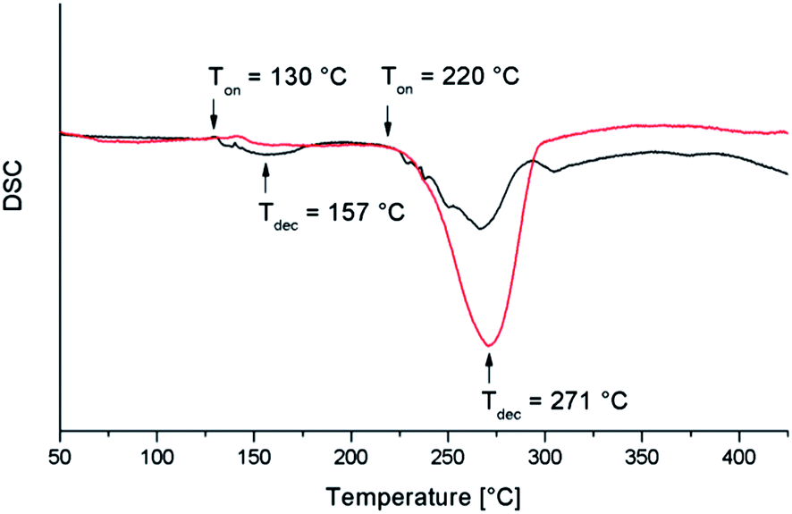 | ||
| Fig. 2 DSC curves of Et2Te2 (black curve) and Et2Te (red curve). | ||
Sb2Te3 films were grown on polycrystalline Al2O3(0001) substrates at substrate temperatures between 350 and 400 °C using a home-made MOCVD cold-wall reactor and a deposition time of 15 minutes. An almost linear increasing growth rate with increasing substrate temperature was found in the temperature range from 350 °C to 400 °C, reaching 750 nm in 15 min at 400 °C. These findings point to a kinetically-controlled growth process, which we have also recently reported for the MOCVD deposition of Sb2Te3 films using (Et2Sb)2Te as a single source precursor.56 The chemical composition (EDX) and the crystallinity (XRD) of the resulting Sb2Te3 films were not affected by the increasing substrate temperature, whereas the morphology of the Sb2Te3 films changed significantly. Sb2Te3 films deposited at 350 °C (Fig. 3a) and 375 °C (Fig. 3b) show a polycrystalline surface, most likely resulting from the low diffusion rates of adatoms as was observed with (Et2Sb)2Te.47 In contrast, very smooth Sb2Te3 films were obtained at 400 °C (Fig. 3c). The substrate material also has a distinguished influence on the film morphology since the deposition on Si(100) substrates at 400 °C only yielded polycrystalline Sb2Te3 films (Fig. 3d).
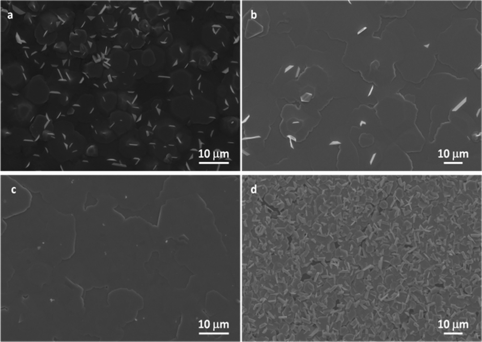 | ||
| Fig. 3 SEM images of the Sb2Te3 film deposited at 350 °C (a), 375 °C (b) and 400 °C (c) on Al2O3(0001) and on Si(100) (d) substrates. | ||
The substrate typically affects the morphology of the growing film. Epitaxial films are preferentially grown on substrates which exhibit a small lattice mismatch (<7%) in order to reduce the lattice strain (so-called hetero-epitaxy).60 However, since Sb2Te3 adopts a rhombohedral crystal structure, in which five monoatomic sheets in a sequence of Te–Sb–Te–Sb–Te are bonded in the c-axis direction, the Sb2Te3 films are always Te-terminated due to the weak van der Waals Te–Te bond. As a consequence, epitaxial V2VI3 films such as Sb2Te3, Bi2Se3 or Bi2Te3 have been grown on substrates with large lattice mismatches such as GaAs, Si(111) and Al2O3(0001), respectively, since the merely attached Sb2Te3 epilayers can achieve their own lattice parameters from the beginning of the growth.61 This growth mechanism is typically referred to as van der Waals epitaxy,62 which explains the formation of epitaxial Sb2Te3 films on Al2O3(0001). In contrast, Sb2Te3 films obtained on Si(100) always showed Sb2Te3 nanodisks of hexagonal shape perpendicular to the surface (Fig. 3d). Comparable findings were previously reported for Bi2Se3 films grown on Si(001).63 The authors suggested that generating the nanodisks on the Bi2Se3 film is energetically more favorable than thickening the film.
Wang et al. showed that the substrate temperature is a key parameter for the MBE growth of high quality Sb2Te3 films on Al2O3(0001) substrates,60 since both the reaction rate and the reaction kinetics are strongly influenced. The composition and surface morphology of the Sb2Te3 films was found to strongly depend on the substrate temperature. High-quality MBE grown films were obtained at 330 °C, whereas lower substrate temperatures gave Sb-deficient films due to the higher sticking coefficient of Te at low temperatures compared to that of Sb. Since the sticking coefficient of Te decreases at higher substrate temperatures, stoichiometric Sb2Te3 films were formed. However, Periano et al. also reported on the MBE growth of stoichiometric Sb2Te3 films at a substrate temperature of 250 °C.64 Herein, we deposited highly stoichiometric Sb2Te3 films at 350 °C and at 400 °C. The film obtained at 400 °C is very flat, consisting of large Sb2Te3 flakes, whereas that obtained at 350 °C also showed hexagonal Sb2Te3 nanocrystals, which adopt orientations perpendicular to the film surface. The higher substrate temperature not only influences the decomposition kinetics of the precursor molecules, resulting in higher decomposition rates, but also affects the mobility of the adatoms, which increases with increasing substrate temperature, yielding larger Sb2Te3 nanoflakes. Moreover, the surface morphology (flatness) of the film improved with the increasing substrate temperature.
SEM (Fig. 4) and AFM micrographs (Fig. 5) of the Sb2Te3 film deposited on Al2O3(0001) substrates at 400 °C within 15 minutes prove the formation of smooth Sb2Te3 films over a large range (substrate dims. 10 × 10 mm). These results were confirmed by cross-sectional SEM microscopy (Fig. 5), showing a uniformly grown Sb2Te3 film of about 750 nm thickness.
 | ||
| Fig. 4 SEM images of the Sb2Te3 film deposited at 400 °C on Al2O3(0001). Bright spots result from small holes in the film. | ||
 | ||
| Fig. 5 Cross-sectional SEM image of a Sb2Te3 film deposited at 400 °C on an Al2O3(0001) substrate showing the layered structure of the Sb2Te3 film. The substrate orientation is tilted by about 15°. | ||
The AFM micrograph (Fig. 6) shows regular terraces of 1 nm height, which correspond to one quintuple layer of the layered tetradymite-type structure of Sb2Te3.65 These findings indicate a layered growth as was also observed in MBE-grown Sb2Te3 thin films.66 Sb2Te3 crystallizes in the space group R![[3 with combining macron]](https://www.rsc.org/images/entities/char_0033_0304.gif) m-D3d5 and forms a layered, rhombohedral crystal structure.67 It is built of anisotropic layers, in which five atomic planes are covalently bonded to the quintuple layer, that is roughly 1 nm thick and consists of five mono-atomic planes of Te(1)–Sb–Te(2)–Sb–Te(1) with 1 and 2 designating the different positions within the fivefold layer. The conventional unit cell includes three quintuple layers, which are bound by weak van der Waals forces.
m-D3d5 and forms a layered, rhombohedral crystal structure.67 It is built of anisotropic layers, in which five atomic planes are covalently bonded to the quintuple layer, that is roughly 1 nm thick and consists of five mono-atomic planes of Te(1)–Sb–Te(2)–Sb–Te(1) with 1 and 2 designating the different positions within the fivefold layer. The conventional unit cell includes three quintuple layers, which are bound by weak van der Waals forces.
 | ||
| Fig. 6 AFM photograph of a Sb2Te3 film deposited at 400 °C on an Al2O3(0001) substrate. | ||
The chemical composition of the material film was analyzed by EDX analysis. Almost perfect Sb2Te3 films with the expected 40:60 (Sb:Te) molar ratios were found (standard deviation ±0.5 (Sb) and ±1.0 (Te)). Fig. 7 shows an Sb2Te3-film at an early stage of growth. The SEM image shows single plates which are not fully coalesced. The corresponding element mapping by scanning Auger electron microscopy (SAES) shows a homogeneous distribution of Sb and Te within the Sb2Te3 plates. In addition, some carbon impurities are located between the Sb2Te3 plates on the substrate surface.
 | ||
| Fig. 7 SEM (a) and SAES study (mapping of C (b), Sb (c) and Te (d)) of an Sb2Te3 film deposited at 400 °C on (0001) Al2O3 substrates; high element concentrations are indicated by bright colour. | ||
The X-ray diffractogram (XRD) of the Sb2Te3 film deposited at 400 °C (Fig. 8) clearly proved the formation of highly crystalline Sb2Te3 films. All reflection peaks can be indexed on the basis of the structure of rhombohedral Sb2Te3. In addition, a small reflex of the Al2O3(0001) substrate is visible at 41.6°. The peaks in the diffractogram correspond to (001) planes, pointing to a c-axis oriented growth as was previously reported for Sb2Te3 films grown by MBE,68–70 and MOCVD,40–42 respectively.
 | ||
| Fig. 8 2θ XRD pattern of the Sb2Te3 film deposited at 400 °C on an Al2O3(0001) substrate; peaks are labelled (JCPDS-ICDD card 15-0874); the asterisk (*) corresponds to the Al2O3(0001) substrate. | ||
We have characterized the band structure of the surface by photoelectron spectroscopy (PES) after transfer to the photoelectron spectrometer and in situ preparation. To the best of our knowledge, this is the first time that angle-resolved photoemission spectroscopy (ARPES) studies have been performed on MOCVD-grown Sb2Te3 thin films. The PE spectrum in Fig. 9 shows Sb and Te core-levels without any shifted components similar to that of Bi2Se3.71
 | ||
| Fig. 9 Core-level photoemission characterization of the in situ prepared surface. Satellite peaks are not observed. | ||
The overview ARPES spectra of the valence band in Fig. 10 show intense structures around 0.8 eV binding energy and more faint features near EF which are well discernible at 16 and 17 eV photon energy but not at 21 eV, where their photoemission intensity is weak due to final state effects. Fig. 11 shows, therefore, the range near EF for photon energies from 16 to 18 eV displaying the topological surface state. This surface state has previously been studied theoretically9 and in ARPES experiments at selected photon energies (21.2 eV),10,72 55 eV,11 8.44 and 24 eV,72 respectively.
 | ||
| Fig. 10 Overview ARPES spectra of the valence band. The topological surface state forming a Dirac cone near the Fermi level (0 eV binding energy) is best observed at 16 eV photon energy. Another surface state with massive character appears as the higher binding energy and is best seen at 21 eV. | ||
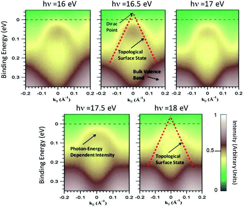 | ||
| Fig. 11 Magnified spectra on the dependence of the topological surface state (Dirac cone) on the photon energy. The dashed line is a linear fit to the data at 16.5 eV and results in a Dirac point ≈30 meV above the Fermi level (hole doping). This Fermi level position means bulk transport according to band structure calculations. | ||
While experiments on cleaved bulk samples led to the conclusion that the Fermi level does not cut the surface state,73 epitaxial Sb2Te3/Si(111) films observed slight hole doping (Dirac point ≈100 meV above EF) and, after deposition of 0.1 monolayer Cs, the undoped state with the Dirac point at EF. The spin texture of the surface state has been probed by spin- and angle-resolved photoemission, and an additional, topologically protected, Rashba-split surface state was found.11 These results have been confirmed recently for epitaxial Sb2Te3/Si(111) films.72 In Fig. 10, this additional surface state is marked at 0.4–0.8 eV binding energy in the data taken at 21 eV photon energy. Due to its high binding energy, it does not contribute to transport. On the other hand it has been found to be much more surface localized than the topological surface state that forms the Dirac cone and its sharp, intense dispersing photoemission features here indicate the presence of a well ordered and stoichiometric surface.
Changing the photon energy in ARPES allows us principally to vary the perpendicular component of the electron wave vector, kz.74 In this way, we can distinguish three-dimensional dispersing features from two-dimensional features. The identical E vs.k|| dispersion in Fig. 11 proves the two-dimensional character. The intensity, however, is subject to the kz-dependence of the parent bulk band structure, and this is seen at 18 eV as a shift of maximum intensity so that at 22 eV (not shown) the surface state is not discernible any longer. The intensity seen near the Fermi energy at 16 eV moves with increasing photon energy to lower binding energy and has crossed EF at 18 eV. This intensity stems directly from bulk valence band states which exist in the complete lower Dirac cone up to the Dirac point as is evident from, e.g., surface-projected bulk band calculations.11 Due to these states, the topological transport regime will require the Fermi level to be in the upper Dirac cone. The linear dispersion predicted by theory has been fitted to the data at 16.5 eV in Fig. 11. Extrapolation of the data yields a Fermi velocity of (2.72 ± 0.14) × 105 m s−1, roughly in agreement with previous measurements from single crystals [(3.8 ± 0.2) × 105 m s−1] and density functional theory (3.2 × 10⁵ m s−1),11 and a Dirac point ≈30 meV above EF. The surface is, therefore, slightly hole doped. The calculation shows that bulk valence band states reach up to the Dirac point so that hole doping indicates that the Fermi level cuts through bulk valence band states rendering the transport bulk like.11
Electrical measurements were performed with a PPMS-system (DynaCool QuantumDesign) using the standard Electronic Transport Option. By applying an alternate current of 1 mA with a frequency of 12.2 Hz and a sampling rate of 0.5 s−1, the resistance was measured in the range of 4 to 400 K with a heating rate of 10 K min−1. By making equally spaced 4-point contacts and choosing the contact spacing much larger than the film thickness, the sheet resistivity can be calculated by the following equation:75

I is the applied current at the outer contacts and V is the measured voltage drop between the inner contacts.
The measured sheet resistivity (Fig. 12) shows a metallic like behaviour with a dominating contribution of the carrier transport in the bulk, and a monotonic increase with increasing temperature as was previously observed for ALD-grown Sb2Te3 thin films.24 Here the sheet resistance increases by one order of magnitude (10×) over the temperature range from 2 to 400 K, whereas the resistance of the ALD film increased moderately by the factor of 1.5 over the same temperature range. The MOCVD films exhibit a higher carrier concentration (>1019 cm−3) correlated with intrinsic defects, most likely antisite defects as is common for Sb2Te3. Furthermore, we assume that the carrier concentration is nearly constant over the complete temperature range and the strong enhancement of the resistance over temperature is related to the reduction of the carrier mobility. Due to the high doping concentration the enhancement of the carrier concentration by thermal excitation of carriers over the bulk-bandgap is not observed by the resistance curve (Fig. 12) or has a negligible impact. In the case of ALD grown Sb2Te3 films a stabilisation of the resistance at least around 350 K has been reported.24
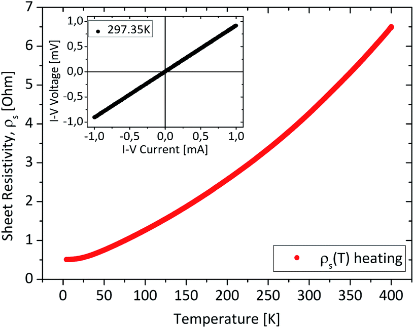 | ||
| Fig. 12 Resistivity against temperature. The inset graph shows the I–V-curve measured at room temperature with 1 mA at 12.2 Hz. | ||
Conclusions
The layer-by-layer MOCVD deposition of highly crystalline Sb2Te3 films was achieved at substrate temperatures between 350 and 400 °C using i-Pr3Sb and Et2Te2. Even though both precursors start to decompose at lower temperatures as was shown by DSC, higher temperatures are necessary in order to produce smooth and crystalline Sb2Te3 films. The film growth occurs under kinetic control, reaching deposition rates as high as 3 μm per hour at 400 °C. The electrical sheet resistivity was found to monotonically increase with increasing temperature. ARPES measurements for the first time showed the detailed dispersions of the bulk valence band and the topological surface state for MOCVD grown Sb2Te3 films with a quality no less than for optimized bulk single crystals. The surface state dispersion gives a Dirac point roughly 30 meV above the Fermi level leading to hole doping and the presence of bulk valence states at the Fermi energy. Additional Bi doping of the Sb2Te3 films is currently under investigation in order to further modify the valence band and the topological surface states.Acknowledgements
Stephan Schulz (StS), Oliver Rader (OR) and Kornelius Nielsch (KN) acknowledge financial support by the DFG (priority program SPP 1666), the University of Duisburg-Essen (StS), the Karl-Vossloh-Stiftung (KN), and the University of Hamburg (KN). Partha Sarathi Mandal is supported by the Impuls- und Vernetzungsfonds der Helmholtz-Gemeinschaft. The authors like to thank PD Dr Nils Hartmann, University of Duisburg-Essen, for SAES studies.Notes and references
- R. Venkatasubramanian, E. Siivola, T. Colpitts and B. O'Quinn, Nature, 2001, 413, 597 CrossRef CAS PubMed.
- T. C. Harman, P. J. Taylor, M. P. Walsh and B. E. LaForge, Science, 2002, 297, 2229 CrossRef CAS PubMed.
- D. Hsieh, Y. Xia, D. Qian, L. Wray, F. Meier, J. H. Dil, J. Osterwalder, L. Patthey, A. V. Fedorov, H. Lin, A. Bansil, D. Grauer, Y. S. Hor, R. J. Cava and M. Z. Hasan, Phys. Rev. Lett., 2009, 103, 146401 CrossRef CAS.
- H. Zhang, C.-X. Liu, X.-L. Qi, X. Dai, Z. Fang and S.-C. Zhang, Nat. Phys., 2009, 5, 438 CrossRef CAS.
- L. He, X. Kou and K. L. Wang, Phys. Status Solidi RRL, 2013, 7, 50 CrossRef CAS.
- J. J. Cha, K. J. Koski and Y. Cui, Phys. Status Solidi RRL, 2013, 7, 15 CrossRef CAS.
- J. Moore, Nat. Phys., 2009, 5, 378 CrossRef CAS.
- X.-L. Qi, R. Li, J. Zang and S.-C. Zhang, Science, 2009, 323, 1184 CrossRef CAS PubMed.
- H. Zhang, C.-X. Liu, X.-L. Qi, X. Dai, Z. Fang and S.-C. Zhang, Nat. Phys., 2009, 5, 438 CrossRef CAS.
- G. Wang, X. Zhu, J. Wen, X. Chen, K. He, L. Wang, X. Ma, Y. Liu, X. Dai, Z. Fang, J. Jia and Q. Xue, Nano Res., 2010, 3, 874 CrossRef CAS PubMed.
- C. Pauly, G. Bihlmayer, M. Liebmann, M. Grob, A. Georgi, D. Subramaniam, M. R. Scholz, J. Sánchez-Barriga, A. Varykhalov, S. Blügel, O. Rader and M. Morgenstern, Phys. Rev. B: Condens. Matter Mater. Phys., 2012, 86, 235106 CrossRef.
- B. Zhou, Y. Ji, Y. F. Yang, X. H. Li and J. H. Zhu, Cryst. Growth Des., 2008, 8, 4394 CAS.
- G.-H. Dong, Y.-J. Zhu and L.-D. Chen, CrystEngComm, 2011, 13, 6811 RSC.
- J. Chen, T. Sun, D. H. Sim, H. Peng, H. Wang, S. Fan, H. H. Hng, J. Ma, F. Y. C. Boey, S. Li, M. K. Samani, G. C. K. Chen, X. Chen, T. Wu and Q. Yan, Chem. Mater., 2010, 22, 3086 CrossRef CAS.
- L. M. Goncalves, C. Couto, P. Alpuim, D. M. Rowe and J. H. Correia, Mater. Sci. Forum, 2006, 514–516, 156 CrossRef CAS.
- B. Lv, S. Hu, W. Li, X. Di, L. Feng, J. Zhang, L. Wu, Y. Cai, B. Li and Z. Lei, Int. J. Photoenergy, 2010, 476589, DOI:10.1155/2010/476589.
- A. M. Farid, H. E. Atyia and N. A. Hegab, Vacuum, 2005, 80, 284 CrossRef CAS PubMed.
- K. Ulutas, D. Deger and S. Yakut, J. Phys.: Conf. Ser., 2013, 417, 012040 CrossRef.
- G. Hao, X. Qi, G. Wang, X. Peng, S. Chang, X. Wei and J. Zhong, RSC Adv., 2012, 2, 10694 RSC.
- G. Hao, X. Qi, Y. Fan, L. Xue, X. Peng, X. Wei and J. Zhong, Appl. Phys. Lett., 2013, 102, 013105 CrossRef PubMed.
- L. M. Goncalves, P. Alpuim, A. G. Rolo and J. H. Correia, Thin Solid Films, 2011, 519, 4152 CrossRef CAS PubMed.
- S. Meister, H. Peng, K. Mcllwrath, K. Jarausch, X. Zhang and F. Y. Cui, Nano Lett., 2006, 6, 1514 CrossRef CAS PubMed.
- J. S. Lee, S. Brittman, D. Yu and H. Park, J. Am. Chem. Soc., 2008, 130, 6252 CrossRef CAS PubMed.
- S. Zastrow, J. Gooth, T. Boehnert, S. Heiderich, W. Toellner, S. Heimann, S. Schulz and K. Nielsch, Semicond. Sci. Technol., 2013, 28, 035010 CrossRef.
- Q. Huang, A. J. Kellock and S. Raoux, J. Electrochem. Soc., 2008, 155, D104 CrossRef CAS PubMed.
- M. Y. Kim, K. W. Park and T. S. Oh, J. Korean Phys. Soc., 2008, 53, 266 CAS.
- D. Pinisetty, M. Gupta, A. B. Karki, D. P. Young and R. V. Devireddy, J. Mater. Chem., 2011, 21, 4098 RSC.
- I. Y. Erdogan and U. Demir, J. Electroanal. Chem., 2009, 633, 253 CrossRef CAS PubMed.
- I.-J. Yoo, Y. Song, D. Chan Lim, N. V. Myung, K. Hyoung Lee, M. Oh, D. Lee, Y. Do Kim, S. Kim, Y.-H. Choa, J. Yul Lee, K. Hwan Lee and J.-H. Lim, J. Mater. Chem. A, 2013, 1, 5430 CAS.
- J.-H. Lim, M. Yeong Park, D.-C. Lim, N. V. Myung, J.-H. Lee, Y.-K. Jeong, B. Yoo and K. Hwan Lee, Mater. Res. Bull., 2012, 47, 2748 CrossRef CAS PubMed.
- J.-H. Lim, M. Yeong Park, D.-C. Lim, B. Yoo, J.-H. Lee, N. V. Myung and K. Hwan Lee, J. Electron. Mater., 2011, 40, 1321 CrossRef CAS PubMed.
- T. Chen, P. Fan, Z. Zheng, D. Zhang, X. Cai, G. Liang and Z. Cai, J. Electron. Mater., 2012, 41, 679 CrossRef CAS PubMed.
- B. Fang, Z. Zeng, X. Yan and Z. Hu, J. Mater. Sci.: Mater. Electron., 2013, 24, 1105 CrossRef CAS.
- N. Peranio, M. Winkler, D. Bessas, Z. Aabdin, J. Koenig, H. Böttner, R. P. Hermann and O. Eibl, J. Alloys Compd., 2012, 521, 163 CrossRef CAS PubMed.
- G. Wang, X. Zhu, J. Wen, X. Chen, K. He, L. Wang, X. Ma, Y. Liu, X. Dai, Z. Fang, J. Jia and Q. Xue, Nano Res., 2010, 3, 874 CrossRef CAS PubMed.
- T. J. Groshens, Jr, R. W. Gedridge and C. K. Lowe-Ma, Chem. Mater., 1994, 6, 727 CrossRef.
- R. Venkatasubramanian, T. Colpitts, E. Watko, M. Lamvik and N. El-Masry, J. Cryst. Growth, 1997, 170, 817 CrossRef CAS.
- B. Aboulfarah, A. Mzerd, A. Boulouz, A. Giani, A. Foucaran and A. Boyer, Moroccan J. Condens. Matter, 1998, 1, 100 Search PubMed.
- A. Giani, A. Boulouz, F. Pascal-Delannoy, A. Foucaran, E. Charles and A. Boyer, Mater. Sci. Eng., B, 1998, 64, 19 CrossRef.
- R. Venkatasubramanian, T. Colpitts, B. O'Quinn, S. Liu, N. El-Masry and M. Lamvik, Appl. Phys. Lett., 1999, 75, 1104 CrossRef CAS PubMed.
- A. Giani, A. Boulouz, F. P. Delannoy, A. Foucaran, A. Boyer, B. Aboulfarah and A. Mzerd, J. Mater. Sci. Lett., 1999, 18, 541 CrossRef CAS.
- J. H. Kim, Y. C. Jung, S. H. Suh and J. S. Kim, J. Nanosci. Nanotechnol., 2006, 6, 3325 CrossRef CAS PubMed.
- J.-H. Kim, S.-D. Kwon, D.-Y. Jeong, B.-K. Ju, S.-J. Yoon and J.-S. Kim, 25th Internat. Conf. on Thermoelectrics, 2006 (ICT '06), pp. 411–413. DOI:10.1109/ict.2006.331284.
- J. S. Lee, S. Brittman, D. Yu and H. Park, J. Am. Chem. Soc., 2008, 130, 6252 CrossRef CAS PubMed.
- H. B. Singh and N. Sudha, Polyhedron, 1996, 15, 745 CrossRef CAS.
- J. S. Ritch, T. Chivers, M. Afzaal and P. O'Brien, Chem. Soc. Rev., 2007, 36, 1622 RSC.
- G. Bendt, S. Schulz, S. Zastrow and K. Nielsch, Chem. Vap. Deposition, 2013, 19, 235 CrossRef CAS.
- S. S. Garje, D. J. Eisler, J. S. Ritch, M. Afzaal, P. O'Brien and T. Chivers, J. Am. Chem. Soc., 2006, 128, 3120 CrossRef CAS PubMed.
- R.-Y. Kim, H.-G. Kim, K.-W. Park, J.-K. Ahn and S.-G. Yoon, Chem. Vap. Deposition, 2009, 15, 296 CAS.
- R.-Y. Kim, H.-G. Kim and S.-G. Yoon, J. Appl. Phys., 2007, 102, 083531 CrossRef PubMed.
- R.-Y. Kim, H.-G. Kim and S.-G. Yoon, Appl. Phys. Lett., 2006, 89, 102107 CrossRef PubMed.
- D. W. Kisker, M. L. Steigerwald, T. Y. Kometani and K. S. Jeffers, Appl. Phys. Lett., 1987, 50, 1681 CrossRef CAS PubMed.
- W. M. Li, C. Y. Chen and R. M. Cohen, J. Cryst. Growth, 1995, 156, 343 CrossRef CAS.
- M. Wieber, Sb Organoantimony Compounds Part 1, in Gmelin Handbook of Inorganic Chemistry, ed. H. Bitterer, Springer Verlag, Berlin, 8th edn, 1981 Search PubMed.
- K. Hamada and H. Morishita, Synth. React. Inorg. Met.-Org. Chem., 1981, 11, 597 CrossRef CAS.
- D. W. Kisker, M. L. Steigerwald, T. Y. Kometani and K. S. Jeffers, Appl. Phys. Lett., 1987, 50, 1681 CrossRef CAS PubMed.
- K. J. Irgolic, Organotellurium Compounds, in Houben-Weyl's Methods' of Organic Chemistry, ed. D. Klamann, Georg Thieme Verlag, Stuttgart, 1991, vol. E12b Search PubMed.
- F. O. Rice and A. L. Glasebrook, J. Am. Chem. Soc., 1934, 56, 2472 CrossRef CAS.
- H. B. Singh and P. K. Khanna, J. Organomet. Chem., 1988, 338, 9 CrossRef CAS.
- G. Wang, L. Endicott and C. Uher, Sci. Adv. Mater., 2011, 3, 539 CrossRef CAS PubMed.
- Y. Takagaki, B. Jenichen, U. Jahn, Y. Manzke, M. Ramsteiner and K.-J. Friedland, Semicond. Sci. Technol., 2013, 28, 025012 CrossRef.
- A. Koma, K. Sunouchi and T. MiyaJima, Microelectron. Eng., 1984, 2, 129 CrossRef CAS; O. Lang, R. Schlaf, Y. Tomm, C. Pettenkofer and W. Jägermann, J. Appl. Phys., 1994, 75, 7805 CrossRef PubMed.
- Y. Takagaki, B. Jenichen, U. Jahn, M. Ramsteiner, K.-J. Friedland and J. Lähnemann, Semicond. Sci. Technol., 2011, 26, 125009 CrossRef.
- N. Periano, M. Winkler, Z. Aabdin, J. Koenig, H. Böttner and O. Eibl, Phys. Status Solidi A, 2012, 209, 289 CrossRef.
- K. M. F. Shahil, M. Z. Hossain, V. Goyal and A. A. Balandin, J. Appl. Phys., 2012, 111, 054305 CrossRef PubMed.
- Y. Jiang, Y. Y. Sun, M. Chen, Y. Wang, Z. Li, C. Song, K. He, L. Wang, X. Chen, Q.-K. Xue, X. Ma and S. B. Zhang, Phys. Rev. Lett., 2012, 108, 066809 CrossRef.
- W. Richter, H. Köhler and C. R. Becker, Phys. Status Solidi B, 1977, 84, 619 CrossRef CAS.
- B. Aboulfarah, D. Sayah, A. Mzerd, A. Giani and A. Boyer, Moroccan J. Condens. Matter, 2000, 3, 76 Search PubMed.
- L. W. da Silva, M. Kaviany and C. Uher, J. Appl. Phys., 2005, 97, 114903 CrossRef PubMed.
- B. Huang, C. Lawrence, A. Gross, G.-S. Hwang, N. Ghafouri, S.-W. Lee, H. Kim, C.-P. Li, C. Uher, K. Najafi and M. Kaviany, J. Appl. Phys., 2008, 104, 113710 CrossRef PubMed.
- M. R. Scholz, J. Sánchez-Barriga, D. Marchenko, A. Varykhalov, A. Volykhov, L. V. Yashina and O. Rader, Phys. Rev. Lett., 2012, 108, 256810 CrossRef CAS.
- L. Plucinski, A. Herdt, S. Fahrendorf, G. Bihlmayer, G. Mussler, S. Döring, J. Kampmeier, F. Matthes, D. E. Bürgler, D. Grützmacher, S. Blügel and C. M. Schneider, J. Appl. Phys., 2013, 113, 053706 CrossRef PubMed.
- D. Hsieh, Y. Xia, D. Qian, L. Wray, F. Meier, J. H. Dil, J. Osterwalder, L. Patthey, A. V. Fedorov, H. Lin, A. Bansil, D. Grauer, Y. S. Hor, R. J. Cava and M. H. Hasan, Phys. Rev. Lett., 2009, 103, 146401 CrossRef CAS.
- Angle Resolved Photoemission, ed. S. D. Kevan, Elsevier, Amsterdam, 1992 Search PubMed.
- F. M. Smits, Bell Syst. Tech. J., 1958, 37, 371 CrossRef (same as BT Monograph, 3894, Part 2).
| This journal is © The Royal Society of Chemistry 2014 |