 Open Access Article
 This Open Access Article is licensed under a
 Creative Commons Attribution 3.0 Unported Licence
Controlling the nanostructure of bismuth telluride by selective chemical vapour deposition from a single source precursor†
Sophie L.
Benjamin
a,
C. H. (Kees)
de Groot
b,
Chitra
Gurnani
a,
Andrew L.
Hector
a,
Ruomeng
Huang
b,
Elena
Koukharenko
b,
William
Levason
a and
Gillian
Reid
*a
aChemistry, University of Southampton, Southampton, SO17 1BJ, UK. E-mail: G.Reid@soton.ac.uk
bElectronics and Computer Science, University of Southampton, Southampton, SO17 1BJ, UK
First published on 12th February 2014
Abstract
High quality, nanostructured Bi2Te3, with an unprecedented degree of positional and orientational control of the material form on the nanoscale, is readily obtained by low pressure chemical vapour deposition using a new molecular precursor. This system offers a convenient method that delivers key structural requirements necessary to improve the thermoelectric efficiency of Bi2Te3 and to develop the nascent field of topological insulators.
Thermoelectric (TE) materials are widely regarded to have the potential to revolutionise electrical power generation and cooling by dramatically reducing the inefficiency of current methods and thus reducing global dependency on fossil fuels. Current coal, natural gas, oil, and nuclear power generation processes are typically only ∼40% efficient and it is estimated that if a further 1% of their primary energy could be recovered, ∼190 TW h of electricity would be generated annually within the EU, with a market value of >€19bn and significant associated reductions in CO2 emissions.1 However, improving thermoelectric efficiency of current materials is a key barrier to wider adoption of this emerging technology.
Bismuth telluride (Bi2Te3), a layered semiconductor with a narrow band gap of 0.16 eV,2 and its alloys are commonly used in commercial bulk thermoelectric (TE) devices as they have among the best room temperature thermoelectric properties of known bulk materials.3 While solid state TE technology has the potential to deliver sustainable and highly durable energy generation, it is currently used only in niche applications. This is due to the low efficiency (∼12% for commercially available devices) and relatively high cost of manufacturing of the current generation of TE materials. However, it has been demonstrated that nanostructuring of TE materials can lead to significant increases in efficiency, due to both quantum confinement effects and reductions in lattice thermal conductivity, i.e. decoupling between the electron scattering (electrical conductivity) and phonon scattering (thermal conductivity).4 Thus modern TE theory predicts that the efficiency of a TE device can be increased by a factor of ca. 3 if the diameter can be decreased in size to that at which quantum confinement and interface scattering effects occur.5 It has also been established that preferred orientation of the nanocrystalline Bi2Te3 such that heat flow is in the 〈1 1 0〉 plane maximises its TE properties.6
Additionally, there is considerable interest in methods to deposit individual single crystals of Bi2E3 (E = Te, Se) with specific orientations as topological insulators, containing protected surface quantum conduction states.7 Such materials have potential applications in quantum computing. Importantly, confinement of these crystals on the nanoscale gives the best surface to volume ratio and optimisation of this effect.8
For both of these applications there is therefore significant motivation to develop methods capable of selectively depositing individual, high quality, nanocrystalline materials such as Bi2Te3 onto surfaces in predetermined positions and with a high degree of orientational control.
Electrodeposition has been the subject of intense research activity as it is currently the only potential method of achieving such control over Bi2Te3 deposition.9 Chemical vapour deposition (CVD) is an attractive alternative process and is widely used in the industrial manufacture of semiconductor thin films, due to its simple and scalable nature.10 Bi2Te3 thin films have previously been deposited on large surfaces by dual source CVD using trialkylbismuth and dialkyltelluride gases as precursors.11,12 The use of molecular, single source precursors for CVD can give advantages in the control of film stoichiometry and morphology, as well as ease of handling.13 We recently reported the first use of a metal telluroether precursor in low pressure (LP) CVD of Ga2Te3,14 and have also demonstrated the growth of 2D micron-scale arrays of metal selenide semiconductor materials by LPCVD from selenoether complexes, exploiting substrate selectivity to achieve area selective deposition.15,16 Huang and co-workers have also identified a strong substrate influence in the vapour deposition of layered chalcogenide nanoplates.17 However, no single source precursors for the CVD of Bi2Te3 are currently known, although deposition of Sb2Te3 nanoplates has been demonstrated from [Sb{(Te PiPr2)2N}3].18
Here we report the deposition of individual nanocrystals of Bi2Te3via a one-step LPCVD method that allows positional control on the nanometre scale. By exploiting the selectivity of the deposition onto TiN surfaces over SiO2, arrays of microcrystalline Bi2Te3 thin films were deposited into TiN wells in lithographically patterned SiO2/TiN substrates, with no deposition on the surrounding SiO2. In larger (>500 nm) diameter wells, films were generally polycrystalline, with a high degree of 〈0 0 1〉 preferred orientation of the hexagonal crystallites (i.e. the c-axis aligns perpendicular to the TiN surface). In contrast, for wells of 100 to 500 nm diameter, individual nanocrystals are produced; SEM shows that these have the opposite orientation, with each crystallite contacting through a crystal edge to the TiN surface with the c-axis parallel to the substrate surface, hence exhibiting 〈1 1 0〉 preferred orientation (Fig. 1).
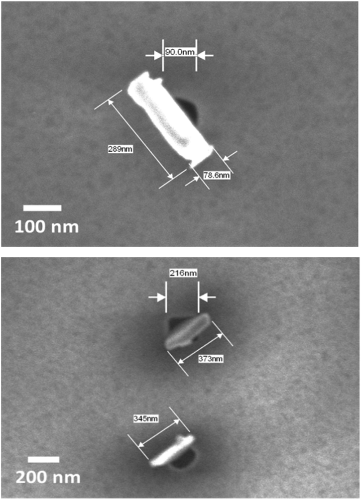 | ||
| Fig. 1 Individual nanocrystals of Bi2Te3 contacting through a crystal edge to the TiN surface within 100 (top) and 200 nm (bottom) wells on a TiN/SiO2 patterned substrate, resulting in 〈1 1 0〉 preferred orientation. | ||
The high quality of the Bi2Te3 deposited by LPCVD from the new reagent was established from thin films grown onto larger SiO2 and TiN surfaces under a range of conditions. Both the thin films and the arrays of Bi2Te3 were characterised by X-ray diffraction (XRD), scanning electron microscopy (SEM), energy dispersive X-ray spectroscopy (EDX), Raman spectroscopy and wavelength dispersive X-ray spectroscopy (WDX) to establish composition, purity, crystal structure and morphology. Hall effect and Seebeck coefficient measurements were also performed to evaluate the thermoelectric performance.
The new molecular precursor [BiCl3(TenBu2)3], a very rare example of a bismuth telluroether complex, was prepared and characterised as described.‡ It is a dark red oil which is highly moisture sensitive and mildly thermally sensitive, though it is stable for long periods stored under N2 at −18 °C. Thermogravimetric analysis (TGA) (Fig. S1, ESI†) was undertaken as a guide to the LPCVD conditions. SEM images of Bi2Te3 films grown by LPCVD onto SiO2 or TiN from ca. 50 mg of [BiCl3(TenBu2)3] at 500 °C, 0.05 mm Hg, show continuous films of pseudo-hexagonal platelets, most of which lie flat on the surface of the substrate (Fig. S2, ESI†).
Hall effect measurements conducted on polycrystalline films deposited onto insulating SiO2 substrates show that for films of thickness ca. 1.0 μm, the resistivity was (5.65 ± 0.02) × 10−4 Ω·cm. The Bi2Te3 is n-type with a carrier concentration of 1.95 × 1020 cm−3, and a mobility of 56.6 cm2 V−1 s−1. Seebeck effect measurements were performed on the same Bi2Te3 sample in order to evaluate the potential performance for TE applications. The mean Seebeck coefficient was −109 μV K−1, consistent with films of n-type conductivity. These data are comparable with values reported previously for thin films of Bi2Te3 grown by other thin film technologies, such as MOCVD,12 molecular beam epitaxy (MBE),19 co-sputtering20 and electrodeposition.21 Importantly, their transport properties, carrier concentrations and Hall mobility values are also close to the range of optimum values that are required for thermoelectric applications.22
Micro- and nano-patterning and selectivity
A similar LPCVD method was employed using patterned SiO2/TiN substrates, which have SiO2 surfaces containing arrays of photolithographically etched wells (1 μm deep, 1–100 μm diameter) giving access to a TiN surface exposed at their base. Under carefully controlled conditions Bi2Te3 was deposited into these TiN wells with excellent substrate selectivity, the wells being filled with crystals, but with no deposition being observed on the surrounding SiO2 capping layer (Fig. 2). An important parameter is the quantity of precursor employed: an excess caused overfilling of the holes and was accompanied by some deposition onto the SiO2 layer, whereas too little precursor resulted in incomplete filling. However, careful control of the quantity of reagent allows a continuous film to be deposited within each well. Lowering the temperature of deposition from 500 to 450 °C reduced the crystallite size although, as expected, the time required for complete deposition was increased. Lowering the temperature further (to 400 °C) resulted in very little material being deposited. | ||
| Fig. 2 Arrays of Bi2Te3 crystals grown by CVD selectively on the TiN surfaces of patterned substrates, (a) 40–10 microns, (b) 10–3 microns, (c) magnified image of 100 micron well. | ||
To investigate the applicability of this technique toward nanostructuring of Bi2Te3 materials, it was necessary to decrease the dimensions of the wells further. e-Beam lithography was used to introduce nanowells between 100 and 500 nm in diameter on the patterned TiN/SiO2 substrate; the thickness of the SiO2 layer was reduced to 200 nm to maintain a reasonable aspect ratio. LPCVD onto these substrates at 450 °C resulted in selective growth of a single nanocrystal into each of the smaller wells. The crystals lie flat in the base of the wells with diameter of ≥1 μm (Fig. 3a), whereas in those of 100–200 nm diameter the individual crystallite size is larger than the wells in which they sit (generally 200–500 nm across and less than 100 nm thick). SEM images (Fig. 1) show that almost all of the crystals in these smallest wells stand on end, apparently contacting through a crystal edge to the TiN surface within the well, but occupying a larger footprint above the substrate. The orientation of crystallites in ≤200 nm wells is ca. 90° to those in the ≥1 μm wells. In the intermediate 500 nm wells both behaviours were observed (Fig. 3b and c). This can be correlated with the size of the nanocrystal relative to the diameter of the well, suggesting that the change to 〈1 1 0〉 preferred orientation reduces the less favourable interactions of the larger Bi2Te3 crystals with the SiO2 walls – see Fig. 3b.
 | ||
| Fig. 3 (a): SEM image of single nanocrystals occupying a 2 micron diameter well, showing the 〈0 0 1〉 preferred orientation; (b) image of nanocrystals on Bi2Te3 occupying 500 nm wells on a TiN/SiO2 patterned substrate, showing the 〈1 1 0〉 preferred orientation; (c) image of a Bi2Te3 nanocrystal that is significantly smaller than the 500 nm well, showing the 〈0 0 1〉 orientation; (d) a larger single crystal located within a 200 nm well showing strongly preferred 〈0 0 1〉 preferred orientation. | ||
Excellent selectivity was maintained even on the nanoscale, with very few crystals observed outside of the wells, although around 20–25% of the nanowells appear to be empty. This switching of the preferred orientation simply by reducing the dimensions of the recessed TiN regions is extremely unusual, and, coupled with the demonstrated ability to selectively grow crystalline Bi2Te3 in predetermined areas, offers exciting prospects for increasing the TE efficiency of Bi2Te3 using this new precursor and LPCVD method.
XRD
Symmetric (θ–2θ) XRD data were collected for films deposited onto SiO2 and TiN at 500 °C and into 40–100 μm TiN wells on a patterned substrate at 450 °C. The XRD patterns identify trigonal (R![[3 with combining macron]](https://www.rsc.org/images/entities/char_0033_0304.gif) m) Bi2Te3 as the only phase present. The refined lattice parameters are in good agreement with literature data23 and are presented in Table S1.† However, relative peak intensities differ significantly compared to literature values for bulk Bi2Te3, indicating strongly preferred c-axis orientation of the crystallites. The identification of this preferred orientation is consistent with the SEM images. The degree of preferred orientation varies between films deposited onto different substrates (Fig. 4), with the highest degree of orientation observed from microfocus XRD from individual filled wells in the micro-scale arrays (ESI†). These XRD patterns display only 0 0 l reflections (Fig. 4a). Pole figure measurements were made for two reflections on the same sample, over a larger region of filled wells. The pole figure taken with 2θ = 49.80°, corresponding to the 0 0 15 reflection, exhibits a single, very sharp peak (FWHM ∼ 1°) at the centre of the figure, with α = 90° (Fig. 5a). The figure taken with 2θ = 27.67°, corresponding to the 0 1 5 reflection, exhibits a narrow ring with α = 32° (Fig. 5b). These results are consistent with a highly preferred crystallite orientation with the substrate perpendicular to the c-axis (calculated values of α in this case are 90.0° for any 0 0 l reflection and 32.1° for the 0 1 5 – see Eqn (S1)†). It is probable that the high degree of orientation observed here is not inherent to the patterning, but rather that the flattest crystallite orientation is observed in a thin but continuous film, which are also the conditions that yield the highest degree of selectivity, as discussed above.
m) Bi2Te3 as the only phase present. The refined lattice parameters are in good agreement with literature data23 and are presented in Table S1.† However, relative peak intensities differ significantly compared to literature values for bulk Bi2Te3, indicating strongly preferred c-axis orientation of the crystallites. The identification of this preferred orientation is consistent with the SEM images. The degree of preferred orientation varies between films deposited onto different substrates (Fig. 4), with the highest degree of orientation observed from microfocus XRD from individual filled wells in the micro-scale arrays (ESI†). These XRD patterns display only 0 0 l reflections (Fig. 4a). Pole figure measurements were made for two reflections on the same sample, over a larger region of filled wells. The pole figure taken with 2θ = 49.80°, corresponding to the 0 0 15 reflection, exhibits a single, very sharp peak (FWHM ∼ 1°) at the centre of the figure, with α = 90° (Fig. 5a). The figure taken with 2θ = 27.67°, corresponding to the 0 1 5 reflection, exhibits a narrow ring with α = 32° (Fig. 5b). These results are consistent with a highly preferred crystallite orientation with the substrate perpendicular to the c-axis (calculated values of α in this case are 90.0° for any 0 0 l reflection and 32.1° for the 0 1 5 – see Eqn (S1)†). It is probable that the high degree of orientation observed here is not inherent to the patterning, but rather that the flattest crystallite orientation is observed in a thin but continuous film, which are also the conditions that yield the highest degree of selectivity, as discussed above.
 | ||
| Fig. 4 X-ray diffraction patterns from symmetric scans of Bi2Te3 films deposited on various substrates. (a): Bi2Te3 contained in a 100 μm diameter well on a TiN/SiO2 patterned substrate; (b): deposited onto a flat SiO2 substrate; (c): deposited onto a flat TiN substrate; (d): indexed literature pattern generated by ICSD from ref. 21. | ||
 | ||
| Fig. 5 Pole figures with cut line graphs for the 0 0 15 (2θ = 49.80°) (a) and 0 1 5 (2θ = 27.67°) (b) reflections of an array of Bi2Te3 deposited on a TiN/SiO2 patterned substrate (1–100 μm diameter). Note that the 4 spots on the inner edge of the ring in (b) correspond to Si (1 1 1) from the substrate. | ||
EDX spectroscopy of the films and micro-scale arrays of Bi2Te3 gave a consistent Bi![[thin space (1/6-em)]](https://www.rsc.org/images/entities/char_2009.gif) :Te ratio of 2:3 (40.31% Bi, 59.69% Te), measured quantitatively against a reference sample of Bi2Te3 (99.99%, Strem Chemicals) (Fig. 6). In the case of the single nanocrystals, EDX measurements also identified Bi and Te, but the low signal relative to that from the substrate precluded accurate determination of the Bi:Te ratio. Raman spectra on both the flat films and the nanocrystals identified them as Bi2Te3 (ref. 24) (Fig. 7 and S3†).
:Te ratio of 2:3 (40.31% Bi, 59.69% Te), measured quantitatively against a reference sample of Bi2Te3 (99.99%, Strem Chemicals) (Fig. 6). In the case of the single nanocrystals, EDX measurements also identified Bi and Te, but the low signal relative to that from the substrate precluded accurate determination of the Bi:Te ratio. Raman spectra on both the flat films and the nanocrystals identified them as Bi2Te3 (ref. 24) (Fig. 7 and S3†).
 | ||
| Fig. 6 EDX data for a Bi2Te3 thin film deposited onto a SiO2 substrate. | ||
 | ||
| Fig. 7 Raman spectrum of Bi2Te3 nanocrystal array within 200 nm wells. The broad features to high frequency are from the substrate. | ||
WDX analysis on the thin films allowed better peak resolution, and confirmed the absence of any peaks in the region of Cl Kα (2.621 keV) or O Kα (0.525 keV) (Fig. S4a†). A small peak is observed at 0.28 keV which is likely to have contributions from C Kα (0.277 keV) and the weaker Bi N6–N5 peak (0.284 keV), however these peaks could not be resolved by WDX (Fig. S4b†). In order to determine the C content in these films, combustion analysis was undertaken on samples of Bi2Te3 that were removed from the substrate by scraping. The C atom content was below 0.5%.
Conclusions
We have demonstrated that regular arrays of high quality single Bi2Te3 nanocrystals can be deposited by LPCVD from a single source bismuth chloride telluroether complex with a very high degree of positional control, and that the preferred orientation of the nanocrystals is strongly governed by the dimensions of the underlying micro- or nano-patterned substrate. The ability to achieve such a high level of control over topology for Bi2Te3 offers exciting prospects for developing this system for thermoelectric applications, and towards topological insulators. We expect that this approach could be extended to the synthesis of nanocrystalline arrays of other key semiconductor materials by the judicious choice of molecular precursors.Acknowledgements
We thank the EPSRC for support (EP/I010890/1), for provision of the thin film X-ray diffraction instrument (EP/K009877/1) and for a Doctoral Prize (S.L.B.). We also thank the Royal Society for a Newton International Fellowship (C.G.), Dr Yudong Wang for assistance with preparing the lithographically patterned substrates and Mr A. Clark for help with the WDX measurements.Notes and references
- Materials for Emerging Energy Technologies, EC Report, ed. J. V. Benesch, 2012, http://ec.europa.eu/research/industrial_technologies/pdf/emerging-materials-report_en.pdf Search PubMed.
- T. C. Harman, B. Paris, S. E. Miller and H. L. Goering, J. Phys. Chem. Solids, 1957, 2, 181–190 CrossRef CAS.
- L. E. Bell, Science, 2008, 321, 1457–1461 CrossRef CAS PubMed; G. J. Snyder and E. S. Toberer, Nat. Mater., 2008, 7, 105–114 CrossRef PubMed.
- C. J. Vineis, A. Shakouri, A. Majumdar and M. G. Kanatzidis, Adv. Mater., 2010, 22, 3970–3980 CrossRef CAS PubMed; A. J. Minnich, M. S. Dresselhaus, Z. F. Ren and G. Chen, Energy Environ. Sci., 2009, 2, 466–479 Search PubMed.
- L. D. Hicks, T. C. Harman and M. S. Dresselhaus, Appl. Phys. Lett., 1993, 63, 3230–3232 CrossRef CAS PubMed.
- X. A. Fan, J. Y. Yang, W. Zhu, S. Q. Bao, X. K. Duan, C. J. Xiao and K. Li, J. Alloys Compd., 2008, 461, 9–13 CrossRef CAS PubMed; I. J. Ohsugi, T. Kojima, M. Sakata, M. Yamanashi and I. A. Nishida, J. Appl. Phys., 1994, 76, 2235–2239 CrossRef PubMed.
- H. Zhang, C.-X. Liu, X.-L. Qi, X. Dai, Z. Fang and S.-C. Zhang, Nat. Phys., 2009, 5, 438–442 CrossRef CAS.
- H. Peng, K. Lai, D. Kong, S. Meister, Y. Chen, X.-L. Qi, S.-C. Zhang, Z.-X. Shen and Y. Cui, Nat. Mater., 2010, 9, 225–229 CAS.
- C. Boulanger, J. Electron. Mater., 2010, 39, 1818–1827 CrossRef CAS PubMed; E. Koukharenko, X. Li, I. Nandhakumar, N. Frety, S. P. Beeby, D. Cox, M. J. Tudor, B. Schiedt, C. Trautmann, A. Bertsch and N. M. White, J. Micromech. Microeng., 2008, 18, 104015 CrossRef; A. J. Naylor, E. Koukharenko, I. S. Nandhakumar and N. M. White, Langmuir, 2012, 28, 8296–8299 CrossRef PubMed; X. Li, E. Koukharenko, I. S. Nandhakumar, J. Tudor, S. P. Beeby and N. M. White, Phys. Chem. Chem. Phys., 2009, 11, 3584–3590 RSC.
- A. C. Jones and M. L. Hitchman, in Chemical Vapour Deposition: Precursors, ed. A. C. Jones and M. L. Hitchman, The Royal Society of Chemistry, 2009, pp. 1–36 Search PubMed.
- A. Giani, A. Boulouz, F. Pascal-Delannoy, A. Foucaran, E. Charles and A. Boyer, Mater. Sci. Eng., B, 1999, 64, 19–24 CrossRef CAS; R. Venkatasubramanian, T. Colpitts, E. Watko, M. Lamvik and N. El-Masry, J. Cryst. Growth, 1997, 170, 817–821 CrossRef.
- H. You, S. Hyub Baek, K.-C. Kim, O. J. Kwon, J.-S. Kim and C. Park, J. Cryst. Growth, 2012, 346, 17–21 CrossRef CAS PubMed.
- M. A. Malik, M. Afzaal and P. O'Brien, Chem. Rev., 2010, 110, 4417–4446 CrossRef CAS PubMed.
- K. George, C. H. de Groot, C. Gurnani, A. L. Hector, R. Huang, M. Jura, W. Levason and G. Reid, Chem. Mater., 2013, 25, 1829–1836 CrossRef CAS.
- C. H. de Groot, C. Gurnani, A. L. Hector, R. Huang, M. Jura, W. Levason and G. Reid, Chem. Mater., 2012, 24, 4442–4449 CrossRef CAS.
- S. L. Benjamin, C. H. de Groot, C. Gurnani, A. L. Hector, R. Huang, K. Ignatyev, W. Levason, S. J. Pearce, F. Thomas and G. Reid, Chem. Mater., 2013, 25, 4719–4724 CrossRef CAS PubMed.
- L. Huang, Y. Yu, C. Li and L. Cao, J. Phys. Chem. C, 2013, 117, 6469–6475 CAS.
- S. S. Garje, D. J. Eisler, J. S. Ritch, M. Afzaal, P. O'Brien and T. Chivers, J. Am. Chem. Soc., 2006, 128, 3120–3121 CrossRef CAS PubMed.
- N. Peranio, M. Winkler, D. Bessas, Z. Aabdin, J. König, H. Böttner, R. P. Hermann and O. Eibl, J. Alloys Compd., 2012, 521, 163–173 CrossRef CAS PubMed.
- X. Wang, H. He, N. Wang and L. Miao, Appl. Surf. Sci., 2013, 276, 539–542 CrossRef CAS PubMed.
- M. M. Rashid, K. H. Cho and G.-S. Chung, Appl. Surf. Sci., 2013, 279, 23–30 CrossRef CAS PubMed.
- D. M. Rowe, Handbook of Thermoelectrics, CRC Press, Boca Raton 1995 Search PubMed.
- A. Adam, Mater. Res. Bull., 2007, 42, 1986–1994 CrossRef CAS PubMed.
- D. Teweldebrhan, V. Goyal and A. A. Balandin, Nano Lett., 2010, 10, 1209–1218 CrossRef CAS PubMed.
- E. G. Hope, T. Kemmitt and W. Levason, Organometallics, 1988, 7, 78–83 CrossRef CAS.
Footnotes |
| † Electronic supplementary information (ESI) available: Details of substrate preparation and characterisation of the Bi2Te3 thin films; thermogravimetric analysis (TGA) of [BiCl3(TenBu2)3], SEM images of thin films of Bi2Te3, Raman analysis of Bi2Te3 thin films, WDX compositional analysis of Bi2Te3 thin films, and microfocus and pole figure XRD analysis of micro-scale Bi2Te3 arrays, lattice parameters refined for Bi2Te3 grown on different substrates. See DOI: 10.1039/c4ta00341a |
| ‡ Precursor preparation and characterisation: reactions were conducted using Schlenk, vacuum line and glove-box techniques under a dry nitrogen atmosphere. The reagents were stored and manipulated using a glove box. MeCN was dried over CaH2. nBuLi was obtained from Acros and used as received. TenBu2 was prepared according to the literature method.25 Infrared spectra were recorded as Nujol mulls between CsI plates using a Perkin-Elmer Spectrum100 spectrometer over the range 4000–200 cm−1. 1H, 13C{1H} and 125Te{1H} NMR spectra were recorded at 298 K in CDCl3 using a Bruker DPX400 spectrometer and referenced to the residual solvent resonance and neat TeMe2 respectively. Microanalyses were undertaken by Medac Ltd. [BiCl3(TenBu2)3]: BiCl3 (0.15 g, 0.48 mmol) was dissolved in MeCN (10 mL) and the solution cooled to 0 °C. A solution of TenBu2 (0.35 g, 1.44 mmol) in MeCN (10 mL) was slowly added to the cooled BiCl3 solution causing an immediate orange colour which darkened to red. After stirring the solution at 0 °C for 30 min, the volatile components were removed in vacuo, leaving a viscous red oil which was dried in vacuo. Yield: 0.39 g, 79%. 1H NMR: δ = 0.96 (t, [3H], CH3), 1.46 (m, [2H], CH2), 1.81 (q, [2H], CH2), 3.24 (t, [2H], CH2Te); 13C{1H} NMR: δ = 11.9, 13.5, 25.1, 33.6; 125Te{1H} NMR: δ = 238.5. IR (Nujol cm−1): ν = 248 br (Bi–Cl). Anal. calcd for C24H54BiCl3Te3: C 27.7, H 5.2; found: C 27.6, H 5.3%. LPCVD of Bi2Te3: In a typical experiment to grow thin films onto unpatterned substrates, 50 mg of the reagent, followed by the substrate tiles (0.5 × 8 × 20 mm), were loaded into a closed-end silica tube in a glove box. The substrates were positioned end-to-end through the heated zone. The tube was set in the furnace such that the precursor was 2 cm away from the edge of the heated zone. The tube was evacuated (∼0.05 mm Hg), and then heated to 773 K (unpatterned SiO2 or TiN substrates) or 723 K (patterned substrates). After 20 min the tube position was adjusted to move the precursor closer to the heated zone until no more precursor was evaporated, leaving behind a small amount of metallic residue. The tube was then cooled to room temperature under vacuum, the substrates subsequently being unloaded and handled in air. Thin films were deposited onto 2 or 3 of the individual substrates and were silvery grey in appearance. |
| This journal is © The Royal Society of Chemistry 2014 |