 Open Access Article
 This Open Access Article is licensed under a
 Creative Commons Attribution 3.0 Unported Licence
Amorphous and highly nonstoichiometric titania (TiOx) thin films close to metal-like conductivity
Thomas
Leichtweiss
a,
Ralph A.
Henning
a,
Julius
Koettgen
be,
Rüdiger M.
Schmidt
ce,
Bernd
Holländer
de,
Manfred
Martin
be,
Matthias
Wuttig
ce and
Jürgen
Janek
*a
aInstitute of Physical Chemistry, Justus-Liebig-University Giessen, 35392 Giessen, Germany. E-mail: Juergen.Janek@phys.chemie.uni-giessen.de
bInstitute of Physical Chemistry, RWTH Aachen University, 52056 Aachen, Germany
cInstitute of Physics (IA), RWTH Aachen University, 52056 Aachen, Germany
dPeter Grünberg Institut (PGI-9), Forschungszentrum Jülich GmbH, 52425 Jülich, Germany
eJARA-Fundamentals of Future Information Technologies, Germany
First published on 12th February 2014
Abstract
Oxygen-deficient titanium oxide films (TiOx) have been prepared by pulsed laser deposition at room temperature. Samples in their as-deposited state have an average composition of TiO1.6, are optically absorbing and show electronic conductivities in the range of 10 S cm−1. The films are metastable and consist of grains of cubic titanium monoxide (γ-TiO) embedded in an amorphous TiO1.77 matrix. Upon annealing in an argon atmosphere the electrical conductivity of the films increases and comes close to metal-like conductivity (1000 S cm−1) at about 450 °C whereas the local structure is changed: nanocrystalline grains of metallic Ti are formed in the amorphous matrix due to an internal solid state disproportionation. The highly conductive state can be frozen by quenching. During heat treatment in an argon atmosphere a stoichiometric rutile TiO2 surface layer forms due to oxidation by residual oxygen. The combination of a highly conductive TiOx film with such an approximately 20 nm thick rutile cover layer leads to a surprisingly high efficiency for the water-splitting reaction without the application of an external potential.
Introduction
Recently Nagarajan et al. reported that strongly oxygen deficient gallium oxide, GaOx, shows a new type of chemically driven insulator–metal transition, once prepared in an amorphous form by pulsed laser deposition.1,2 In fact, amorphous phases with a composition roughly described by GaO1.2 and with electrically insulating behavior showed conductivity jumps of several orders of magnitude upon heating. This phenomenon is related to an internal redox disproportionation reaction, leading to the precipitation and growth of transparent and insulating Ga2O3 nuclei in the GaOx matrix, which loses even more oxygen. This leads to the increase of the Fermi level such that the GaOx matrix attains metal-like conductivity – caused by an internal solid-state reaction. Petitmangin et al. showed that for highly nonstoichiometric gallium oxide, depending on the deposition conditions, the phase separation could also lead to the precipitation of metallic Ga clusters within a crystalline Ga2O3 matrix.3 This new type of insulator–metal transition in a main group oxide attracts strong interest, and similar phenomena have now been reported also for other oxides, e.g. for indium tin oxide (ITO),4 indium zinc oxide (IZO),5,6 Al incorporated IZO7 and gallium-doped indium oxide.8Here, we report on our successful attempts on finding similar phenomena in highly sub-stoichiometric, i.e. ultra-reduced titanium oxide (TiOx) films prepared by pulsed laser deposition (PLD). As in the case of GaOx we take advantage of the possibility to deposit films with composition and structure far from thermodynamic equilibrium by PLD and show that during heat treatment these films gain electrical conductivity by chemical disproportionation while nanocrystals of TiO and Ti precipitate in the amorphous matrix. In fact, as is shown below, this glass-ceramic TiOx can be quenched such that a highly conducting TiOx film with almost metal-like behavior is obtained. Finally, we present (first) results on the water-splitting abilities of the films, which show surprisingly high efficiencies. We would like to note that – despite intensive work on the Ti–O system and its electrical properties – no comparable results have been published before to our knowledge.
Other than the Ga–O system, the Ti–O system shows many more equilibrium phases and is by far more complex.9 The most important phases and the two most common polymorphs of stoichiometric TiO2 are the anatase and the rutile structures, the latter being thermodynamically stable formed at temperatures of 700 °C to 900 °C.10 In contrast to the above-mentioned gallium–oxygen system, titanium oxide is also well known to exist in a wide range of stoichiometries besides the O/Ti = 2 ratio, such as the crystalline Magnéli phases TinO2n−1 (4 ≤ n ≤ 10),11 which are derived from the rutile structure by crystallographic shear due to the removal of oxygen. Other compounds in the binary titanium–oxygen phase diagram include monoclinic Ti3O5, corundum-type Ti2O3 as well as titanium monoxide TiO – which itself is a highly nonstoichiometric phase. The latter is metallic and has a cubic rock salt (γ-TiO) or monoclinic (α-TiO) structure. All these oxygen deficient crystalline phases (relative to the O/Ti = 2 ratio in TiO2 with Ti(IV) in its [Ar] 3d0 4s0 electron configuration) are fairly good electrical conductors at room temperature, with the highest bulk conductivities of 1000 S cm−1 reported for Ti4O7 and for TiO, respectively.12,13 Semiconductor-to-metal transitions are reported for many of the lower titanium oxides: the transition temperatures of several Magnéli phases lie in the range of 100 K to 200 K (ref. 13) but Ti2O3 and Ti3O5 undergo phase transitions at temperatures above room temperature at about 200 °C.14,15
Besides its enormous practical relevance as a non-toxic white pigment, titanium dioxide has attracted great interest since the discovery of the water-splitting reaction due to the illumination of TiO2 electrodes with UV light in a photoelectrochemical cell16 and due to its photocatalytic properties.17 Furthermore, O'Reagan and Grätzel reported on a high efficiency dye-sensitized solar cell, which contains titanium oxide nanoparticles.18 Undoped TiO2 is a semiconductor with an optical band gap of about 3 eV and as the efficiency of the water-splitting reaction in sunlight strongly depends on the electronic and optical properties of the semiconducting photoelectrode, many works have been devoted to increase the optical absorption of TiO2 in the visible range of the spectrum. Besides doping the titanium or oxygen sublattice with various elements (for a comprehensive review see ref. 19), non-stoichiometry and disorder heavily affect the electronic and therefore optical properties of a material. Chen et al. have recently shown that TiO2 nanocrystals with disordered and reduced surfaces exhibit high solar-driven photocatalytic efficiencies due to the small bandgap of the material.20 In the second part of this paper we demonstrate that also TiOx glass ceramics show good photoanodic behavior, which may still leave room for further improvement.
Switching a material between two states of different electrical conductivities due to the application of an electrical field is the basis for the so-called resistive switching effect, which has recently attracted great attention and could lead to a new generation of non-volatile memory devices. This phenomenon has been known for TiO2 thin films for many years21 and possible devices could be based on metal/TiOx/metal stacks. In a recent review paper, Szot et al. discuss the formation of reduced TiO2 phases in the context of resistive switching.22 Proposed mechanisms for the memristive effect in TiO2 include the formation of localized conduction channels (filaments) on the nanoscale within semiconducting amorphous TiO2 matrices, which have been identified as Magnéli phases (e.g. Ti4O7)23,24 or the valence change of titanium due to redox processes.25
Bulk samples with a large deviation from TiO2 stoichiometry are generally prepared by high temperature reduction of crystalline titania in hydrogen containing atmospheres or by annealing TiO2 together with Ti metal. The preparation of stoichiometric TiO2 films by vacuum based physical vapor deposition methods such as pulsed laser deposition (PLD) or sputter deposition is well established and it is possible, depending on the desired application, to control the ratio of anatase and rutile phases in the deposited films. As one could expect, the stoichiometry of the resulting material critically depends on the oxygen partial pressure p(O2) during the deposition process. Hence, it is possible to directly prepare TiOx films within a wide range of stoichiometries by these methods.26–29 Crystalline films of titanium monoxide can be obtained by low temperature deposition under carefully controlled p(O2).30–32 The preparation of crystalline films with stoichiometries in between 1 < x < 2 (i.e. Ti2O3, Ti3O5 and the Magnéli phases), however, seems to be challenging – probably due to the complicated structures. Only few reports claim the deposition of such phases by sputtering33 or chemical vapour deposition.34 To the best of our knowledge, nothing is known to date about the crystalline phase formation in amorphous and highly oxygen deficient TiOx being heated in non-oxidative atmospheres – which is the subject of the present paper.
Experimental details
Titania films were prepared by pulsed laser deposition (PLD) at room temperature in a commercial vacuum chamber (SURFACE systems+technology GmbH & Co. KG) using a KrF excimer laser (λ = 248 nm, Lambda Physik) operated at a laser fluence of 3 J cm−2 and a repetition rate of 10 Hz. A metallic titanium slab (Goodfellow, 99.99% purity) was used as target material and the target substrate distance was set to 70 mm. Polished sapphire crystals with c-axis orientation (Crystek GmbH) were used as substrates. The vacuum chamber was evacuated to a base pressure of 10−3 Pa prior to deposition, and films were deposited in pure oxygen atmosphere at a pressure of p(O2) = 0.2 Pa. The thicknesses of the films were in the range of 500 nm to 1000 nm as determined with an Alpha-Step IQ profilometer (Lot Oriel). For RBS analysis thinner (d ≈ 100 nm) films were deposited on Si (100) wafers.The chemical composition of the samples was determined by Rutherford backscattering spectrometry (RBS). The samples were irradiated with a 1.4 MeV He+-ion beam for a fixed ion dose of 15 μC at the Jülich 1.7 MV Tandem Accelerator. The backscattered ions were detected at an angle of 170° and the resulting spectra were fitted using the RUMP software.35 The estimated accuracy for the determination of the oxygen content is about ±5%. For electrical characterization, a four-point-probe setup was employed applying the geometrical correction factors calculated by Smits.36 Four equidistant (1 mm) Au-contacts (thickness 200 nm) were deposited by thermal evaporation on top of thin Cr-contacts (thickness 3 nm) onto the samples and connected to a Keithley 2400 SourceMeter. The contacts were proven to be ohmic by checking the linearity of an I–V curve recorded directly after connecting the cell. The samples were heated in a home-built tube furnace under a protective argon atmosphere (Ar flow).
High-resolution transmission electron microscopy (HR-TEM) and selected-area electron diffraction (SAED) were carried out with an analytical transmission electron microscope FEI Tecnai F20 operated at 200 kV. Prior to analysis, crosssections of the films were prepared by focused ion beam (FIB) milling. In order to protect the TiOx film from beam damage and to allow charge neutralization during FIB preparation the samples were subsequently coated with conductive carbon and gold contacts and a tungsten cover layer. The one dimensional circularly averaged intensity distribution of the SAED diffraction patterns has been calculated with the ProcessDiffraction software.37
In situ X-ray diffraction experiments were carried out in a theta/theta diffractometer (STOE & Cie GmbH) which is equipped with a high-temperature chamber (HDK 2.4K, Johanna Otto GmbH) using Cu Kα radiation (λ = 1.5406 Å). The samples have been kept at the respective temperatures for 30 min before data acquisition in order to let them reach thermodynamic equilibrium.
The density of the films was determined by X-ray reflectometry (XRR) using a Siemens D5000 diffractometer and the REFSIM software package.
XPS experiments were performed using a PHI 5000 Versaprobe spectrometer (Physical Electronics). In order to minimize possible re-oxidation, the samples were transferred under a protective Ar atmosphere from the PLD system into the XPS chamber. All spectra were acquired at a chamber pressure in the range of 10−6 Pa using a monochromatized Al X-ray anode (beam diameter 200 μm, X-ray power 50 W). The analyzer was operated at pass energies of 11.75 eV for detail spectra of the Ti 2p and O 1s core levels and of 23.5 eV for the X-ray induced valence band spectra. As the sample surfaces were nearly free of adventitious hydrocarbons, the O 1s line (530.3 eV) was used for calibration of the binding energy scale and, when necessary, background subtraction was performed using the mathematical model derived by Shirley.38 Atomic concentrations were calculated applying the appropriate sensitivity factors provided by the instrument manufacturer.
The photoelectrochemical (PEC) experiments were carried out in a rectangular PMMA reactor (ca. 30 × 50 × 100 mm3) equipped with a quartz window. A two-electrode system was used: a platinum foil counter electrode (300 mm2) and the TiOx electrodes (19.6 mm2) immersed in an aqueous 0.1 M NaOH electrolyte. For the PEC measurements, the TiOx films were coated on commercial ITO glass substrates. Bias supply and current measurements were done by an electrochemical workstation (Parstat 2273, Princeton Applied Research). Measurements of the I–V characteristics were carried out with a scan rate of 2 mV s−1. As a light source, we used a 150 W Xe Arc lamp (Lot Oriel) and a Thermopile (Ophir 3A-P) plus energy monitor (Nova Oriel) for light intensity measurements. The quantum efficiency or incident photon to charge carrier conversion efficiency (IPCE) was measured by illuminating the samples with a monochromatic light beam (monochromator, Lot Oriel, MSH101, width of entrance and exit slit: 2.5 mm). The photocurrent at each wavelength was recorded until the steady state at a constant electrode potential of 0 V was observed (Keithley 6517A Electrometer).
Results
Films deposited under an oxygen partial pressure of 0.2 Pa have a dark blue/gray color and exhibit an electrical conductivity of about 10 S cm−1 at room temperature. The films are compact and flat. They have an average density of 4.65 g cm−3 as determined by X-ray reflectometry (XRR), being far denser than TiO2 (ρ(rutile) = 4.25 g cm−3, ρ(anatase): 3.89 g cm−3). RBS analysis reveals the average ratio Ti![[thin space (1/6-em)]](https://www.rsc.org/images/entities/char_2009.gif) :O to be 1:1.6.
:O to be 1:1.6.
Photoelectron spectroscopy
To obtain insights into the composition of the films, we performed photoelectron spectroscopy. Therefore, the samples were transferred from the deposition chamber to the XP spectrometer without air contact as reduced titanium oxide forms a thin surface oxidation layer when in contact with oxygen even at room temperature. Fig. 1a shows detail spectra of the Ti 2p doublet line of a pristine film. | ||
| Fig. 1 (a) XPS detail spectra of the Ti 2p signal, (b) fitted Ti 2p3/2 and (c) O 1s lines; (d) X-ray induced valence band spectrum of a TiOx film that has been deposited under p(O2) = 0.2 Pa. | ||
Due to partial reduction of titanium dioxide, a broad shoulder appears on the low binding energy (BE) side of the Ti 2p1/2 and Ti 2p3/2 lines. A peak fit analysis of the Ti 2p3/2 signal with mixed Gaussian–Lorentzian profiles (Fig. 1b) reveals two underlying components at binding energies of 458.9 eV and 457.3 eV which represent titanium in its Ti4+ and Ti3+ oxidation states, respectively.39 The photoelectron signal from the O 1s orbitals (Fig. 1c) has a broad shoulder on the high BE side, which can be deconvoluted into two additional signals attributed to O–H bonds from hydroxyl groups or water molecules at the sample surface.40 Both species are present during sample handling (contaminations in the argon gas filled glove-box) and even in the residual gas of the analysis chamber and are known to be easily adsorbed by the highly reactive TiOx film.41 Therefore, only oxygen from the low BE signal at 530.3 eV is bound to titanium and the surface composition can be estimated by applying the appropriate atomic sensitivity factors to the integrated peak areas of the Ti 2p and O 1s (Ti–O) lines to be TiO1.77. This value is higher than the bulk composition determined by RBS (xRBS = 1.6) because the latter method determines the average stoichiometry over the whole film thickness while XPS probes only the topmost surface and is blind for local composition changes deeper in the material as will be shown in the following. Nevertheless, a slight re-oxidation of the surface during glove-box transfer cannot be excluded; therefore the O:Ti ratio of 1.77 should be taken as an upper limit.
Fig. 1d presents the XPS valence band spectrum of the pristine film, which confirms the partial filling of Ti 3d states as can be seen by an electronic state in the band gap at about 1 eV.27
Electrical characterization
Temperature dependent characterization of the electrical properties gives insight into the nature of the conduction mechanisms (semiconducting or metallic behavior) and, moreover, varying slopes in the conductivity vs. temperature diagrams may reveal phase transitions occurring at particular temperatures. In order to prevent the oxidation of reduced metal oxide films such experiments have to be performed under inert gas conditions. We therefore heated our samples in argon gas flow with p(O2) below 10 Pa as controlled by an oxygen sensor. On increasing the temperature of a TiOx sample in its as-prepared state (Fig. 2a) we initially observe a constant rise in the electrical conductivity up to 300 °C (denoted as region “(I)”) clearly showing the semiconducting nature of the pristine film. | ||
| Fig. 2 (a) Electrical conductivity as a function of reciprocal temperature for a TiOx film prepared at p(O2) = 0.2 Pa. After heating up to 600 °C (heating rate 1 K min−1) the sample was kept for 30 min at this temperature before cooling. (b) Natural logarithm of the normalized conductivities of four TiOx films prepared at p(O2) = 0.2 Pa as a function of the reciprocal temperature. The samples were heated to different temperatures (black: 600 °C, red: 360 °C, blue: 260 °C) and afterwards cooled down to room temperature. For better comparison the conductivities are normalized to the respective values at 50 °C. | ||
This behavior has been quantitatively reproduced for several samples deposited under the same experimental conditions as can be seen in Fig. 2b where relative conductivities are shown as a function of the reciprocal sample temperature. In order to eliminate small differences in the absolute conductivities, e.g. due to different qualities of the gold contacts or to errors in the evaluation of the film thicknesses, σ is normalized to the conductivity at 50 °C (σ50). The activation energy in region (I) of 0.17–0.18 eV lies well in range with thermally activated electronic n-type conduction by shallow donors in reduced titania commonly reported at energies of 0.1–0.2 eV below the conduction band.42
Unexpectedly the slopes of the curves change drastically at about 300 °C–310 °C, and the conductivity increases sharply by almost one order in magnitude (region II). In this region the conduction mechanism is changed by the onset of a chemical disproportionation, as discussed below. Note that while slopes and the transition temperature are basically reproduced for all samples it is also obvious that the transition kinetics differ. As will become clear later, the films are extremely sensitive even to small parameter fluctuations during the deposition process and sample analysis.
Upon further heating (III), the slope decreases and again a semiconducting behavior can be observed but the activation energy is significantly smaller than for the pristine film. Conductivity finally reaches a maximum as high as 1000 S cm−1 at roughly 450 °C. During further increase of the temperature and annealing of the sample at 600 °C (IV) for 30 min a strong decrease can be observed. We attribute this drop by more than four orders of magnitude to the full oxidation of the TiO1.6 film to TiO2 by residual oxygen in the argon gas. After annealing at 600 °C the samples are fully transparent and a columnar nanocrystalline rutile phase can be observed by X-ray diffraction (compare Fig. 4) and scanning electron microscopy (not shown). The conductivity decreases further on cooling down the oxidized sample showing the typical behavior of a semiconducting film (region (V) in Fig. 2a). Note, that the conductivity and the activation energy (0.17 eV) of the oxidized sample during cooling are still significantly higher than those reported for nanocrystalline stoichiometric rutile.43 We therefore assume that some reduced states remain after annealing.
The highly conductive state can be frozen by cooling down the sample to room temperature during or shortly after the transition region II (red curve in Fig. 2b). The slope of the cooling curve stays negative (semiconducting behavior) but the observed activation energy of 0.07 eV is much smaller than during heating (I) and similar to values reported for reduced rutile crystals.44 The fact that the metal-like electrical properties (i.e. a high conductivity of about 103 S cm−1 which remains almost constant during cooling) of region (II) persist upon cooling clearly shows that indeed an irreversible phase transformation has been taking place above 300 °C.
By and large these findings are similar to the above mentioned analogous experiment on amorphous highly nonstoichiometric gallium oxides as reported by Nagarajan et al.1 A new type of insulator–metal transition occurs during heating which can be best described as an internal solid state disproportionation reaction – leading to a glass–ceramic composite. However, for the TiOx system the change in electrical conductivity during the phase transition is scarcely one order of magnitude whereas the insulator–metal transition in GaOx leads to conductivity changes of seven orders of magnitude. The highly conductive state is metallic in the case of GaOx while still being semiconducting (with a metal-like absolute value) in the case of TiOx. Nevertheless, we assume that the underlying mechanism is also valid in the titanium–oxygen system.
Structural characterization
To study the evolution of the microstructure during heat treatment an as prepared sample and a film in the highly conductive state were analyzed by means of transmission electron microscopy (TEM). Therefore, we annealed a sample at 360 °C for 30 min under argon flow applying a heating rate of 1 K min−1 (compare Fig. 2b). Fig. 3a, c, d and f show cross-sectional TEM-micrographs of approximately 100 nm thick FIB lamellae of the pristine and of the annealed film, respectively.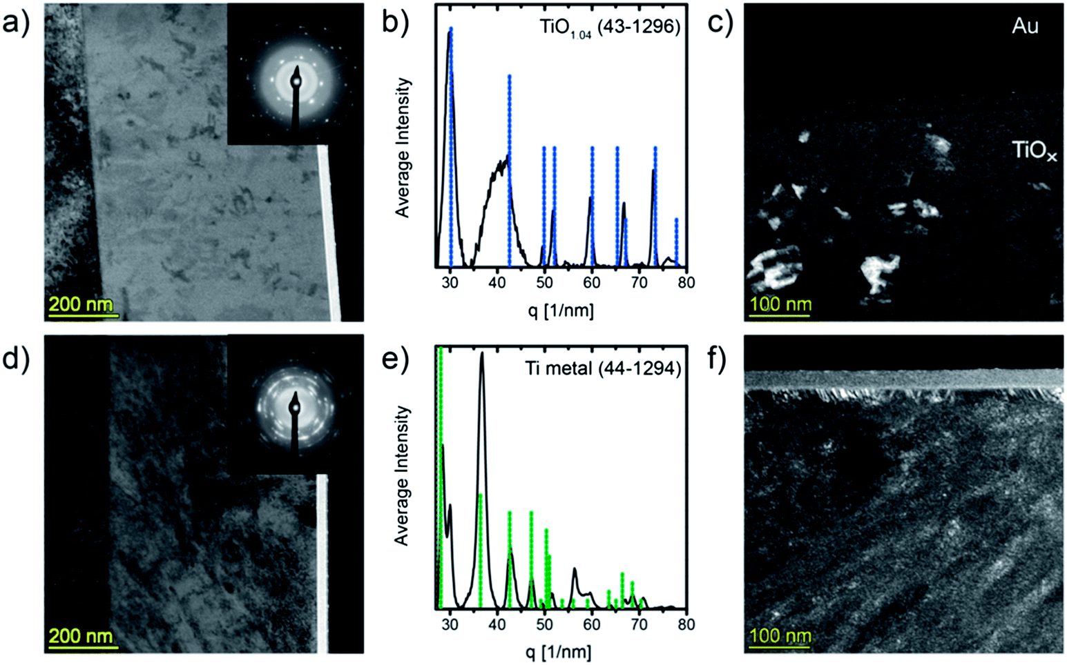 | ||
| Fig. 3 Cross-sectional TEM-micrographs of TiOx films: (a) BF-TEM and (c) DF-TEM of pristine TiOx, (d) BF-TEM and (f) DF-TEM of a film that was annealed at 360 °C. Insets in (a) and (d): SAED patterns of the films. (b and e) Circularly averaged intensity distribution of the SAED pattern and corresponding phases. During preparation of the FIB lamellae the films were coated with an amorphous carbon layer and gold contacts. | ||
It can be seen in the bright field image (Fig. 3a) that the film in its as deposited state is widely homogeneous and contains some regions with higher contrast which can be confirmed to be crystalline by dark field TEM (Fig. 3c). The small crystallites are not connected and appear to be randomly orientated. Selected area electron diffraction (SAED, inset in Fig. 3a) reveals the presence of amorphous (bright halo) and crystalline phases. The one dimensional circularly averaged intensity distribution of the diffraction pattern is shown in Fig. 3b. After background removal, peaks were determined for the non-amorphous region (i.e. for scattering vectors above 27 nm−1). Comparison with the PDF database identifies the crystallites as cubic titanium monoxide (γ-TiO1.04), PDF (43-1296). The TEM images indicate that no γ-TiO crystal extends to the film surface which is well in line with the observation by XPS where no spectral features typical for titanium monoxide45 (i.e. Ti2+ states) could be found. Moreover, the crystals are not connected and therefore the electrical properties reported above are those of the amorphous matrix. We can exclude that the formation of TiO is induced by the electron beam as the crystals are visible over the whole lamellae and no changes as a function of time or of irradiated area could be observed.
The annealing procedure leads to dramatic changes of the film microstructure. As can be seen in Fig. 3d, small nanoparticles featuring high diffraction contrast are formed within the matrix. Even if some of these grains seem to grow diagonally to the substrate normal, no definite texture can be identified. The SAED pattern (Fig. 3e) reveals the sample to consist of metallic titanium (PDF (44-1294)) and, again, a large amorphous fraction can be found as well as an additional reflection at 30 nm−1 that can most likely be assigned to persisting γ-TiO. However, owing to the inhomogeneous and only partly crystalline nature of the material the electron diffraction image is complex and the calculated lines are broad and therefore additional Ti–O phases may remain undetected.
In addition to the microstructural changes in the sample bulk a completely different kind of structure evolves almost perpendicular from the film surface as can be best seen in the DF-TEM image (Fig. 3f). This surface layer seems to grow with columnar microstructure and has a thickness of about 20 nm and a sharp boundary towards the bulk.
To gain insight into the phase formation on a larger scale and to monitor the changes in the crystal structure during thermal treatment, we performed in situ X-ray diffraction experiments under an argon atmosphere. A pristine film was heated and X-ray diffraction patterns were recorded at room temperature and at elevated temperatures up to 600 °C (Fig. 4).
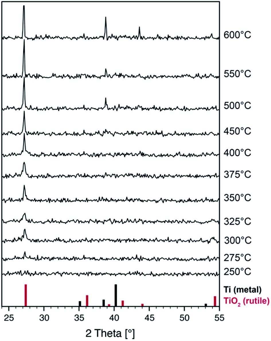 | ||
| Fig. 4 In situ θ–2θ-XRD measurement of a TiOx film (p(O2) = 0.2 Pa during deposition) and powder patterns of TiO2 (rutile structure, PDF file 21-1276) and metallic titanium (PDF file 44-1294). The slight shift of the experimental peak positions relative to the TiO2 pattern is due to small changes in the diffraction geometry during heating. | ||
Surprisingly, neither cubic TiO nor titanium metal can be identified in the pristine and heat treated films by X-ray diffraction. In fact, no Bragg peaks at all can be seen up to temperatures of 250 °C. One possible explanation is that the Ti-metal nanoparticles have crystal sizes below 5 nm as can be determined by high-resolution TEM (not shown) and should hardly be detectable by XRD. Moreover, our setup is optimized for fast data acquisition during thermal treatment at the cost of weak signal intensities.
Crystallization of the rutile TiO2 phase starts at temperatures as low as 275 °C as can be seen by the formation of a peak at 27° which can be attributed to the rutile (110) reflection. Upon further annealing, only this peak grows indicating that the crystal growth occurs with preferred orientation which is well in line with the formation of a textured surface layer in the annealed sample as has been found by TEM. Given the high reactivity of reduced titanium oxides we assume that the film surface is oxidized by residual oxygen in the argon gas. Further reflections of the rutile phase appear above 500 °C when the material is being fully oxidized. The samples are transparent after heat treatment.
RBS analysis of a thinner sample, which has been annealed at 360 °C (same experimental conditions as for TEM analysis) yields a composition of TiO1.7. After taking the surface oxide layer into account (≈20 nm TiO2 on top of 100 nm TiO1.6) we find that the average bulk composition of now TiO1.62 is hardly affected by the heat treatment. Metallic titanium nanocrystals precipitate in the bulk of the film as proven by TEM (i.e. local reduction), we therefore expect simultaneous additionally local oxidation in the bulk of the film.
Photoelectrochemical performance
TiOx films were deposited by PLD onto conductive ITO substrates applying the same process parameters as stated above. The films were then used as anodes in photoelectrochemical (PEC) cells as described in ref. 46. In short, we used a two electrode setup in an aqueous 0.1 M NaOH electrolyte and a xenon arc lamp as an illumination source (150 W). Fig. 5a shows the I–V characteristics of an illuminated TiOx film in its as deposited state and of samples annealed at 360 °C and 460 °C, respectively. The experiments were carried out with a voltage sweep of 2 mV s−1. No side-reactions could be observed in the corresponding dark-currents (not shown).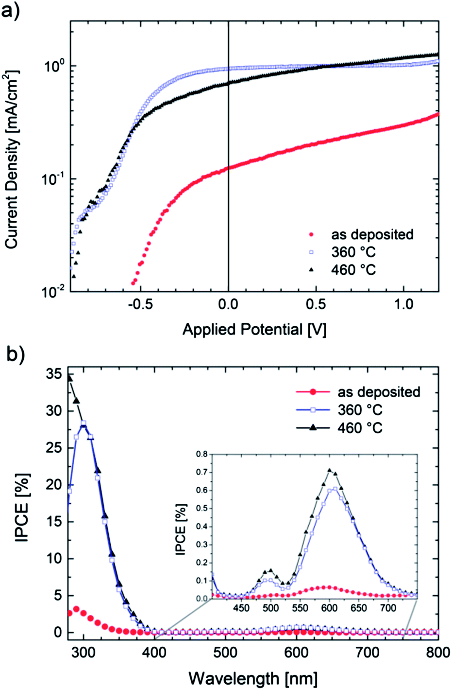 | ||
| Fig. 5 (a) I–V characteristics of TiOx films (scan rate 2 mV s−1) under illumination (375 mW cm−2) and (b) quantum efficiency (IPCE) at Uappl = 0 V. | ||
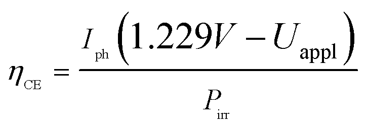
All samples show photoactivity and we observe maximum currents as high as 0.37 mA cm−2, 1.09 mA cm−2 and 1.25 mA cm−2 for the as-deposited, 360 °C and 460 °C annealed films, respectively. The highest short circuit (Uappl = 0 V) current of 0.94 mA cm−2 is obtained for the film annealed at 360 °C. Assuming 100% Faradaic conversion (i.e. all photo-generated charge carriers are utilized for the water-splitting reaction) the conversion efficiency ηCE is defined by
While ηCE is measured during sample illumination with the full spectrum of the light source, the incident photon to current efficiency (IPCE) is useful to determine the wavelength dependent external quantum efficiency of a photoelectrode:
Even though our films are optically highly absorbing in the visible range no red-shift of the photocurrent onset wavelength can be found. Owing to the multi-layered nature of the annealed samples (i.e. 20 nm nanocrystalline rutile TiO2 on a highly conductive glass-ceramic TiOx film annealed at 360 °C) we propose that most of the charge carriers are generated in the surface oxide layer and electrons and holes are effectively separated due to band bending. The remarkable high conversion efficiencies may then be explained by an effective charge transport from the thin TiO2 cover layer into the highly conductive TiOx film. Takahashi et al. found that 70 nm thick TiO2 films have higher water splitting efficiencies than thicker electrodes and argue that – as the space charge region spreads similarly deep into the semiconducting photo-anode – charge separation benefits.49 One could therefore expect that careful variation of the TiO2 thickness might lead to further improved efficiencies but, however, the optimization of the photoanodes lies beyond the scope of this work.
Given the high electronic conductivity of the annealed samples, it should be possible to build up photoelectrochemical cells without a conductive substrate for the TiOx electrode. Note that our samples are almost flat and that efficiencies maybe significantly improved by using electrodes with higher surface areas.
Discussion
The PLD technique allows the preparation of compounds, which are in two points different from the corresponding thermodynamic equilibrium phases: firstly, the composition, in our case the Ti:O ratio, is controlled by the relative fluxes of Ti ions from the target and of oxygen anions in the plasma, the latter being dependent on the oxygen partial pressure in the deposition chamber. Hence, it is possible to prepare phases with compositions that would not occur in equilibrium. Secondly, due to the high deposition rates of PLD, it is possible to prepare metastable phases for compositions which actually also correspond to thermodynamically stable phases in the phase diagram. For the titanium–oxygen system many stable structures are known – mostly being very close in their Gibbs energies.50 Therefore, only small driving forces such as strain-energy or variations in local composition are sufficient to yield metastable TiOx phases.
The average composition of our pristine films (typically about TiO1.6) is close to the known crystalline phases Ti3O5 and Ti2O3. In the case of equilibrium, thermodynamics would predict the coexistence of both phases in our films – or, at low temperatures, Ti4O7 and Ti2O3 should be observed (compare Ti–O phase diagram in Fig. 6b). However, the microstructural analysis has shown that none of the corresponding crystal structures can be found in our freshly prepared films. Instead, a heterogeneous phase mixture of cubic γ-TiO crystals and an amorphous matrix (a-TiOx) with a composition of roughly TiO1.77 has been found (follow the red lines in Fig. 6b). Hence, we conclude that a fully amorphous TiO1.6 phase cannot be maintained in the amorphous state at room temperature and decomposes by a solid state disproportionation reaction within a short time after preparation or already during deposition. The first reaction pathway depicted in the energy and phase diagrams (red lines in Fig. 6a and b) illustrates this decomposition.
 | ||
| Fig. 6 (a) Schematic Gibbs (G) energy diagram (as function of oxygen content) of the disproportionation reactions. (b) Titanium–oxygen phase diagram based on data compiled in ref. 51. | ||
The schematic Gibbs energy diagram may be interpreted with regard to a general formulation of the Ostwald's step rule (OSR): a metastable state relaxes by a series of stepwise transformations into the state with the next highest chemical potential until finally the minimum in free energy is reached. Commonly, this empirical rule is applied for polymorphic transformations, and Ostwald himself had only homogeneous systems in mind when he formulated his rule. In the case of our highly oxygen deficient films, the different free energies of the particular Ti–O compounds act as the main driving force for a series of heterogeneous reactions. As the overall composition remains constant the system relaxes by chemical disproportionation reactions (red line), leading to a heterogeneous phase-mixture which still is metastable. As Schmalzried points out, the OSR may not necessarily apply to such a complex heterogeneous reaction path.52 We also like to note that all reaction paths rely of course on the mobility of ionic and electronic charge carriers. As nothing is known about mobilities (i.e. diffusion coefficients) of charge carriers at comparably low temperatures in highly defective TiOx, we cannot discuss the reaction paths in more depth. But our results indicate that the atomic mobility in nonstoichiometric TiOx might be higher than expected from a simple extrapolation of high temperature data.
Increasing the temperature to a value of 360 °C (following the green reaction path in Fig. 6) leads to the precipitation of metallic Ti nanocrystals, while a major part of the matrix remains amorphous. Hence, it is most likely that metallic titanium forms within the amorphous matrix, which consequently has to be enriched in oxygen leading to the new oxygen-richer amorphous phase a-TiOx+y according to the reaction
The SAED pattern of the annealed film indicates that γ-TiO crystals persist and that further phases – which cannot be unambiguously identified – may have formed during annealing.
It is interesting to note that the films in their as prepared states (i.e. a-TiOx + TiO) have an average density of 4.65 g cm−3, close to the reported values for Ti2O3 (4.59 g cm−3), metallic titanium (4.6 g cm−3) and also close to TiO (4.85–5.1 g cm−3). This is well in line with the identified phases. In contrast, phases richer in oxygen are significantly less dense (Ti3O5: 4.35 g cm−3, Ti4O7 (4.32 g cm−3) and rutile TiO2 (4.23 g cm−3). One possible reason for the fact that no crystalline TinO2n−1 structures (n ≥ 3) can be found is that the required volume change for the formation of these phases is energetically unfavorable in terms of elastic strain energy (i.e. strain energy is greater than the difference in free energy).
The embedded γ-TiO crystals in the as-deposited sample are not connected, therefore electrical characterization yields the conductivity of the semiconducting amorphous matrix. For temperatures higher than 300 °C (region II in Fig. 2) we observe a strong increase in the electrical conductivity of the amorphous matrix indicating the starting point of the second internal decomposition reaction. The highly conductive state can be frozen after heating up to 360 °C and a semiconducting behavior with significantly smaller activation energy is observed on cooling. Thus, the metallic nanocrystals are still too small to form a percolation path at this temperature. As previously stated, the proposed solid state disproportionation should lead to an increase of the oxygen content of the amorphous matrix (a-TiOx+y). This is supported by the fact that the reported electrical conductivities of TinO2n−1 phases do not increase with increasing oxygen non-stoichiometry as one could expect from classical point defect chemistry. Instead, the electrical properties of those phases are dominated by electron correlation effects and the reported room temperature conductivities for bulk crystalline Ti4O7, Ti5O9 or Ti6O11 are significantly higher than those of the more oxygen deficient phases Ti3O5 and Ti2O3.13
It has been clearly shown by TEM and XRD analysis that a crystalline rutile layer is formed in competition with the described internal reactions at the surface during annealing the sample – most probably due to residual oxygen in the protective argon atmosphere. This layer grows with increasing temperature and a strong drop in conductivity occurs when heating beyond the maximal value at roughly 450 °C as rutile TiO2 then forms even below the gold contacts and the samples are eventually fully oxidized.
Conclusions
TiOx films with a composition of roughly TiO1.6 were synthesized by pulsed laser deposition at room temperature. It could be shown by XPS and TEM that the films in their as-deposited state are far from thermodynamic equilibrium as small γ-TiO crystals precipitate in an amorphous TiO1.77 matrix. Annealing of the samples in argon above 300 °C leads to a complex internal phase separation reaction and small titanium nanocrystals precipitate within the material while the amorphous matrix enriches in oxygen. In parallel to this disproportionation reaction a strong increase in the electrical conductivity of the matrix is observed leading to a highly conductive (semiconducting) state that can be frozen by quenching the sample to room temperature.Competitively to the internal solid-state reaction the sample is oxidized by residual oxygen in the argon gas and a columnar rutile cover layer forms on the surface. The combination of a highly conductive TiOx film with an approximately 20 nm thick rutile cover layer yields enhanced photoelectrochemical activity as most charge carriers are generated in the space charge region leading to an effective separation of electrons and holes. Therefore, these multi-layer systems possess high conversion efficiencies for the photocatalytic water-splitting reaction even without applying an external potential.
Acknowledgements
We acknowledge funding by the German Research Foundation (DFG) within the priority program SPP 1415 “crystalline non-equilibrium phases” and within the collaborative research center SFB 917 “Nanoswitches”. The authors thank M. Dietrich for XRR measurements. The authors thank B. Holländer and C. Scholtysik at Peter Grünberg Institut 9, Forschungszentrum Jülich for providing access to the Tandetron ion accelerator.Notes and references
- L. Nagarajan, R. A. De Souza, D. Samuelis, I. Valov, A. Börger, J. Janek, K.-D. Becker, P. C. Schmidt and M. Martin, Nat. Mater., 2008, 7, 391 CrossRef CAS PubMed.
- M. Martin, R. Dronskowski, J. Janek, K.-D. Becker, D. Roehrens, J. Brendt, M. W. Lumey, L. Nagarajan, I. Valov and A. Börger, Prog. Solid State Chem., 2009, 37, 132 CrossRef CAS.
- A. Petitmangin, C. Hebert, J. Perrière, B. Gallas, L. Binet, P. Barboux and P. Vermaut, J. Appl. Phys., 2011, 109, 013711 CrossRef.
- K. Makise, K. Mitsuishi, N. Kokubo, T. Yamaguchi, B. Shinozaki, K. Yano, K. Inoue and H. Nakamura, J. Appl. Phys., 2010, 108, 023704 CrossRef.
- J. Sun and H. Gong, Appl. Phys. Lett., 2010, 97, 092106 CrossRef.
- M. Nistor, J. Perrière, C. Hebert and W. Seiler, J. Phys.: Condens. Matter, 2010, 22, 045006 CrossRef CAS PubMed.
- J. Sun, W. Yang, Y. Huang, W. Soon Lai, A. Y. S. Lee, C. Fu Wang and H. Gong, J. Appl. Phys., 2012, 112, 083709 CrossRef.
- S. L. Wang and L. H. Peng, J. Appl. Phys., 2010, 108, 084503 CrossRef.
- M. Cancarevic, M. Zinkevich and F. Aldinger, CALPHAD: Comput. Coupling Phase Diagrams Thermochem., 2007, 31, 330 CrossRef CAS.
- D. A. H. Hanaor and C. C. Sorrell, J. Mater. Sci., 2011, 46, 855 CrossRef CAS.
- S. Andersson, B. Collen, U. Kuylenstierna and A. Magnéli, Acta Chem. Scand., 1957, 11, 1641 CrossRef CAS.
- S. P. Denker, J. Appl. Phys., 1966, 37, 142 CrossRef CAS.
- R. Bartholomew and D. Frankl, Phys. Rev., 1969, 187, 828 CrossRef CAS.
- C. N. R. Rao, S. Ramdas, R. E. Loehman and J. M. Honig, J. Solid State Chem., 1971, 3, 83 CrossRef CAS.
- C. N. R. Rao, R. E. Loehman and J. M. Honig, Phys. Lett. A, 1968, 27, 271 CrossRef CAS.
- A. Fujishima and K. Honda, Nature, 1972, 238, 37 CrossRef CAS PubMed.
- A. Fujishima, X. Zhang and D. Tryk, Surf. Sci. Rep., 2008, 63, 515 CrossRef CAS.
- B. O'Regan and M. Grätzel, Nature, 1991, 353, 737 CrossRef.
- X. Chen, S. Shen, L. Guo and S. S. Mao, Chem. Rev., 2010, 110, 6503 CrossRef CAS PubMed.
- X. Chen, L. Liu, P. Y. Yu and S. S. Mao, Science, 2011, 331, 746 CrossRef CAS PubMed.
- F. Argall, Solid-State Electron., 1968, 11, 535 CrossRef CAS.
- K. Szot, M. Rogala, W. Speier, Z. Klusek, A. Besmehn and R. Waser, Nanotechnology, 2011, 22, 254001 CrossRef CAS PubMed.
- D. Kwon, K. Kim, J. Jang, J. Jeon, M. Lee, G. Kim, X. Li, G. Park, B. Lee and S. Han, Nat. Nanotechnol., 2010, 5, 148 CrossRef CAS PubMed.
- J. P. Strachan, M. D. Pickett, J. J. Yang, S. Aloni, A. L. David Kilcoyne, G. Medeiros-Ribeiro and R. S. Williams, Adv. Mater., 2010, 22, 3573 CrossRef CAS PubMed.
- D. Jeong, H. Schroeder and R. Waser, Phys. Rev. B: Condens. Matter Mater. Phys., 2009, 79, 195317 CrossRef.
- R. Gouttebaron, D. Cornelissen, R. Snyders, J. P. Dauchot, M. Wautelet and M. Hecq, Surf. Interface Anal., 2000, 30, 527 CrossRef CAS.
- M. C. Marchi, S. A. Bilmes, C. T. M. Ribeiro, E. A. Ochoa, M. Kleinke and F. Alvarez, J. Appl. Phys., 2010, 108, 064912 CrossRef.
- Y. Davila, A. Petitmangin, C. Hebert, J. Perrière and W. Seiler, Appl. Surf. Sci., 2011, 257, 5354 CrossRef CAS.
- N. Sbaï, J. Perrière, W. Seiler and E. Millon, Surf. Sci., 2007, 601, 5649 CrossRef.
- O. Banakh, P. E. Schmid, R. Sanjinés and F. Lévy, Surf. Coat. Technol., 2002, 151–152, 272 CrossRef CAS.
- Z. Li, S. Miyake, M. Makino and Y. Wu, Appl. Surf. Sci., 2008, 255, 2370 CrossRef CAS.
- G. Chen, C. Lee, H. Niu, W. Huang, R. Jann and T. Schütte, Thin Solid Films, 2008, 516, 8473 CrossRef CAS.
- D.-S. Ko, S.-I. Kim, T.-Y. Ahn, S.-D. Kim, Y.-H. Oh and Y.-W. Kim, Appl. Phys. Lett., 2012, 101, 053502 CrossRef.
- R. Tu, G. Huo, T. Kimura and T. Goto, Thin Solid Films, 2010, 518, 6927 CrossRef CAS.
- L. R. Doolitte, Nucl. Instrum. Methods Phys. Res., Sect. B, 1985, 9, 344 CrossRef.
- F. M. Smits, Bell Syst. Tech. J., 1958, 37, 711 CrossRef.
- J. L. Lábár, Microsc. Microanal., 2008, 14, 287 CrossRef.
- D. Shirley, Phys. Rev. B: Solid State, 1972, 5, 4709 CrossRef.
- A. F. Carley, P. R. Chalker, J. C. Riviere and M. W. Roberts, J. Chem. Soc., Faraday Trans. 1, 1987, 83, 351 RSC.
- E. McCafferty and J. P. Wightman, Surf. Interface Anal., 1998, 26, 549 CrossRef CAS.
- J. M. Pan, J. Vac. Sci. Technol., A, 1992, 10, 2470 CAS.
- E. Cho, S. Han, H.-S. Ahn, K.-R. Lee, S. Kim and C. Hwang, Phys. Rev. B: Condens. Matter Mater. Phys., 2006, 73, 193202 CrossRef.
- C. Demetry, Solid State Ionics, 1999, 118, 271 CrossRef CAS.
- H. P. R. Frederikse, J. Appl. Phys., 1961, 32, 2211 CrossRef CAS.
- S. Bartkowski, M. Neumann, E. Kurmaev, V. Fedorenko, S. Shamin, V. Cherkashenko, S. Nemnonov, A. Winiarski and D. Rubie, Phys. Rev. B: Condens. Matter Mater. Phys., 1997, 56, 10656 CrossRef CAS.
- P. Hartmann, D.-K. Lee, B. M. Smarsly and J. Janek, ACS Nano, 2010, 4, 3147 CrossRef CAS PubMed.
- M. Radecka, A. Trenczek-Zajac, K. Zakrzewska and M. Rekas, J. Power Sources, 2007, 173, 816 CrossRef CAS.
- J. F. Houlihan, R. F. Bonaquist, R. T. Dirstine and D. P. Madacsi, Mater. Res. Bull., 1981, 16, 659 CrossRef CAS.
- M. Takahashi, K. Tsukigi, T. Uchino and T. Yoko, Thin Solid Films, 2001, 388, 231 CrossRef CAS.
- A. K. Podshivalova and I. K. Karpov, J. Phys. D: Appl. Phys., 2007, 52, 1147 Search PubMed.
- H. Okamoto, J. Phase Equilib. Diffus., 2011, 32, 473 CrossRef CAS.
- H. Schmalzried, Z. Phys. Chem., 2003, 217, 1281 CrossRef CAS.
| This journal is © The Royal Society of Chemistry 2014 |