
A composition-tunable ZnxCd1−xSe/ZnO core–shell nanowire array: mechanisms for the enhanced charge separation and its photovoltaic applications
Ke Cheng,
Xiao Han,
Jian Meng,
Shujie Wang and
Zuliang Du*
Key Lab for Special Functional Materials of Ministry of Education, Collaborative Innovation Center of Nano Functional Materials and Applications, Henan University, Kaifeng, 475004, Henan Province, P. R. China. E-mail: zld@henu.edu.cn
First published on 23rd December 2014
Abstract
A composition-tunable ZnxCd1−xSe/ZnO (0 < x ≤ 1) core–shell nanowire array has been fabricated on a conductive glass substrate by the hydrothermal growth and the subsequent ion-exchange reaction. The band gap of the ZnxCd1−xSe shell can be readily tuned by adjusting the temperature of the cation exchange reaction. The charge separation and transport ability of the ZnxCd1−xSe@ZnO with different cation exchange temperatures were investigated. Based on the powerful surface photovoltaic spectrum, the mechanism for the enhanced charge separation was discussed and the charge transport model was established. Moreover, the catalytic activities of three different counter electrode materials such as Cu2S, PbS, and Cu2ZnSnS4 were also evaluated based on the ZnxCd1−xSe@ZnO photoanode. Benefitting from the efficient charge separation at the interface of the ZnxCd1−xSe@ZnO core–shell nanowire array and the novel Cu2S counter electrode with a nanowall structure, a maximum photoelectric conversion efficiency of 1.70% has been achieved. Despite the lower conversion efficiency, our findings provided a better understanding of the charge separation and transport properties in type II core–shell heterojunctions.
1. Introduction
Chemical photovoltaic conversion has attracted much interest in the last two decades. Although initial efforts were predominantly focused on the dye-sensitized Grätzel-type solar cells, quantum-dot-sensitized ones have attracted considerable attention recently due to the possibility of exceeding the Shockley–Queisser limit by multiple exciton generation.1–3 An impressive photoelectric conversion efficiency (PCE) as high as 7.04% has been achieved by Juan Bisquert et al.4 In spite of this encouraging achievement, the efficiencies of quantum-dot-sensitized solar cells still lag far behind the dye-sensitized Grätzel-type solar cells (∼11.5%).5 Mesoporous metal oxide nanoparticle films such as TiO2 and ZnO are typically used as photoanodes in the Grätzel-type solar cells. The transport of photogenerated electrons through the network of the nanoparticle film through particle-to-particle hopping is considered to be one of the limiting factors that determine the overall performances.6,7 Such undesirable loss of electrons at grain boundaries via recombination with redox species impedes the efficient transport of electrons to collecting electrode. Fortunately, the electron diffusivity in crystalline nanowires has been reported to be several orders of magnitude larger than that of the nanoparticles film. Therefore, the utilization of one-dimensional (1D) nanowires was considered to be advantageous over the traditional nanoparticle films for its ability to provide direct and efficient pathways for photogenerated carriers.5,8As one of the most important 1D metal oxide nanomaterials, ZnO nanowires (NWs), nanorods and nanofibers have been widely used as photoanode materials in Grätzel-type solar cells.9–12 However, the wide band gap of ZnO (3.37 eV) prevents its efficient light absorption in the visible region, which is responsible for its low energy conversion performance. Various semiconductor QDs with narrow band gaps, such as CdS, CdSe, CdTe, ZnSe, and CuInS2 have been widely used in ZnO nanostructure based solar cells to extend its absorption range to longer wavelengths.13–16 However, the difficulty to distribute the QDs uniformly on ZnO nanostructures, low QD loading density, and interface problems originating from organic linker molecules between the QDs and ZnO nanostructures are still the main bottleneck for improving overall performances. In addition, ZnO is unstable for use in Grätzel-type solar cells with acidic or alkaline electrolyte due to its amphoteric property, which is a major drawback for its practical application.17 Fortunately, the core–shell nanocable ZnO NW has provide the possibility to resolve these problems.18,19 Its absorption profiles can be extend to the visible region due to the suitable lower band gap semiconductor shell on the ZnO NWs core. More importantly, the coaxial core–shell architecture not only enables the carrier extraction across the radius of the ZnO NWs but also the large current injection along the length axial of ZnO NWs. In such type II core–shell heterojunctions, both the valence band maximum (VBMax) and the conduction band minimum (CBMin) in one semiconductor are either lower or higher than its counterparts.20,21 With the stepwise band gap alignment, the electrons and holes can be spatially separated, which will decrease the recombination rate of the electrons and holes.
However, most of the ZnO core–shell heterojunction nanostructures are primarily based on binary semiconductors with fixed composition and band gap.22 In comparison to binary semiconductor shells, ternary semiconductor AxB1−xC/ZnO nanostructures possess continuously tunable physical and optical properties through the variation of its composition. Wang et al. demonstrated that the visible light absorption could be significantly improved by using the ternary ZnSxSe1−x/ZnO core–shell nanostructures.17,23,24 Li et al. prepared a composition-graded ZnxCd1−xSe/ZnO core–shell nanowire array via a temperature gradient chemical vapor deposition (CVD) method, which yielded a continuous absorption edge from 460 nm to 700 nm.22 The ZnxCd1−xSe/ZnO core–shell nanocables were fabricated and used as photoanodes for photoelectrochemical solar cells by Xu et al., which exhibited a better power conversion efficiency.25 Although the ZnxCd1−xSe/ZnO core–shell nanostructures have been synthesized and their photoelectric properties have been evaluated as mentioned above, little research has been focused on the charge separation and transport process at the core–shell interface of ZnxCd1−xSe/ZnO. Therefore, no clear model has been established to illustrate the charge separation and transport process at the core–shell interface without the influences of the liquid electrolyte.
In the current work, the composition-tunable ternary ZnxCd1−xSe/ZnO core–shell NW array was prepared on F-doped SnO2 (FTO) glass substrate by the hydrothermal growth and the subsequent ion-exchange reaction. The light absorption edge of the ZnxCd1−xSe/ZnO core–shell NW array can be readily tuned by regulating the shell composition. As a powerful tool to investigate the photo-induced charge separation and transport at the semiconductor interfaces, the surface photovoltaic spectrum (SPS) was employed to evaluate the charge separation and transport abilities of the samples with different cation exchange reaction temperatures. Based on the SPS results, the model of photo-induced charge separation and transfer was established. The catalytic activities of three different counter electrodes (CEs) materials, including Cu2S, PbS, and Cu2ZnSnS4, were investigated based on the ZnxCd1−xSe/ZnO (140 °C)-polysulfide electrolyte system. The maxium PCE value of 1.70% was obtained, which benefited from the efficient charge separation at the interface of ZnxCd1−xSe/ZnO core–shell NW array and the novel Cu2S nanowall CE.
2. Experimental section
2.1 Preparation of ZnO NWs array
The ZnO NW array was prepared on the FTO substrate using the seed-assisted low temperature hydrothermal method.26 Typically, the pre-cleaned FTO substrates were seeded with the ZnO thin film by spin coating. Then, the ZnO seeded substrates were annealed at 500 °C in air for 3 h. The ZnO seeded FTO substrate was placed in the precursor solution containing 10 mmol L−1 zinc nitrate hexahydrate and 10 mmol L−1 hexamethylene tetramine in a 50 ml Telfon-lined stainless steel autoclave. The autoclave was sealed and heated to 80 °C for 24 h, followed by cooling to room temperature under ambient conditions. The final samples were dried using nitrogen gas after rinsing thoroughly with deionized water. Finally, the ZnO NW array was annealed at 400 °C for 30 min for better crystallinity.2.2 Preparation of ZnxCd1−xSe/ZnO nanocable array
The ZnSe/ZnO core–shell NW array was obtained by a simple anion exchange (Se2−) reaction based on the ZnO NW array.27 In detail, the ZnO NW array was immersed in 30 ml aqueous solution containing 0.015 g of selenium powder and 0.05 g of NaBH4. The selenide process was carried out at 50 °C for 3 h in an oil bath. This process was repeated twice. The final product was rinsed with deionized water to remove the impurities and dried at room temperature. Then, the CdSe/ZnSe/ZnO NW array with bilayer shell was prepared using a cation (Cd2+) exchange reaction.25 The pre-prepared ZnSe/ZnO core–shell NW array was immersed in an aqueous solution containing 0.02 mol L−1 Cd2+ in an autoclave for 10 h. Partial ZnSe was converted to CdSe via cation replacement of Zn2+ by Cd2+. Finally, the ternary ZnxCd1−xSe/ZnO NWs (0 < x ≤ 1) core–shell structure was obtained by annealing the CdSe/ZnSe/ZnO NW array at 400 °C for 30 min in a tube furnace under the protection of argon gas. For the ZnxCd1−xSe/ZnO prepared at 50 °C and 90 °C, the Zn0.7Cd0.3Se and Zn0.33Cd0.67Se were obtained respectively.25 The Zn2+ was replaced by Cd2+ ion completely and the ZnO/CdSe NWs array was obtained when the reaction temperature reached to 140 °C. Further increasing the cation exchange reaction temperature, the CdSe does not form a continuous and uniform shell on the ZnO NWs.2.3 Counter electrodes, polysulfide electrolyte, and the fabrication of solar cells
The Cu2S CE was prepared by immersing a brass sheet in HCl solution (37%) at 70 °C for 10 minutes. Subsequently, the etched brass sheet was dipped into the polysulfide aqueous solution containing 1 mol L−1 Na2S, 1 mol L−1 S−1 and 0.1 mol L−1 NaOH for 10 minutes to form a black Cu2S layer. For the PbS CE, the lead foil was immersed in a mixed solution of H2O and concentrated H2SO4 with a volume ratio of 1![[thin space (1/6-em)]](https://www.rsc.org/images/entities/char_2009.gif) :1 for 24 h at room temperature. The etched lead foil was rinsed with deionized water. Finally, the lead foil was immersed in a polysulfide solution (1 mol L−1 Na2S + 0.1 mol L−1 S−1 + 0.1 mol L−1 NaOH aqueous solution) for 24 h to yield a dark black PbS film on the surface of the lead foil. To examine the effect of non-traditional metallic sulphide CEs, the Cu2ZnSnS4 CE was also prepared by spin coating the Cu2ZnSnS4 sol–gel solution on a pre-cleaned FTO glass substrate.28 The spin-coating step was repeated seven times to obtain the desired film thickness. Finally, the precursor film was vulcanized to fabricate the Cu2ZnSnS4 CE. The polysulfide electrolytes were prepared by dissolving Na2S, S, and NaOH in de-ionized water. The solar cells were fabricated with a sandwich-type by bonding the ZnxCd1−xSe/ZnO photoanode with the different CEs. The two electrodes were separated by a spacer, and the internal space of the cell was filled with the polysulfide electrolyte. The active area was confined by clipping a mask on the photoanode with a square window of 0.2 cm2, and the cells were characterized immediately after the electrolyte filling.
:1 for 24 h at room temperature. The etched lead foil was rinsed with deionized water. Finally, the lead foil was immersed in a polysulfide solution (1 mol L−1 Na2S + 0.1 mol L−1 S−1 + 0.1 mol L−1 NaOH aqueous solution) for 24 h to yield a dark black PbS film on the surface of the lead foil. To examine the effect of non-traditional metallic sulphide CEs, the Cu2ZnSnS4 CE was also prepared by spin coating the Cu2ZnSnS4 sol–gel solution on a pre-cleaned FTO glass substrate.28 The spin-coating step was repeated seven times to obtain the desired film thickness. Finally, the precursor film was vulcanized to fabricate the Cu2ZnSnS4 CE. The polysulfide electrolytes were prepared by dissolving Na2S, S, and NaOH in de-ionized water. The solar cells were fabricated with a sandwich-type by bonding the ZnxCd1−xSe/ZnO photoanode with the different CEs. The two electrodes were separated by a spacer, and the internal space of the cell was filled with the polysulfide electrolyte. The active area was confined by clipping a mask on the photoanode with a square window of 0.2 cm2, and the cells were characterized immediately after the electrolyte filling.
2.4 Characterization
The morphologies of the synthesized samples were characterized by scanning electron microscopy (SEM, JEOL 5600). The structures of the sample were investigated via an X-ray diffractometer (XRD, X'Pert Pro PW3040/60, Holland). The absorption of the samples was determined using a UV-Vis spectrophotometer (HEλIOS, UNICAM). The charge separation and transfer properties at the core–shell interface were measured via the surface photovoltage spectrum (SPS, SR830, Standford). The performances of the solar cells were evaluated under standard AM 1 global illumination using a Newport solar simulator.3. Results and discussion
3.1 Morphology and structural characterization
Fig. 1 shows the typical SEM images of the ZnO NW array and ZnxCd1−xSe/ZnO core–shell NW array. The entire surface of FTO substrate surface was covered with highly uniform and densely packed array of ZnO and ZnxCd1−xSe/ZnO core–shell NWs. The cross-sectional SEM image of pristine ZnO NW array was shown in Fig. 1B. We can see that the ZnO NW array had a tendency to grow perpendicular to the substrate surface with length of about 3 μm. The ZnxCd1−xSe/ZnO core–shell NW array obtained by cation exchange in a Cd2+ aqueous solution at 140 °C retained the overall alignment of the ZnO NW array, as shown in Fig. 1C. The slightly increased diameter and rough surface coating of ZnxCd1−xSe/ZnO core–shell NW array indicating the formation of a core–shell structure, as shown in Fig. 1C and D. The entire surface of the ZnO NWs was covered by the ZnxCd1−xSe shell as shown in Fig. 1D, which was crucial for the formation of type II heterojunction.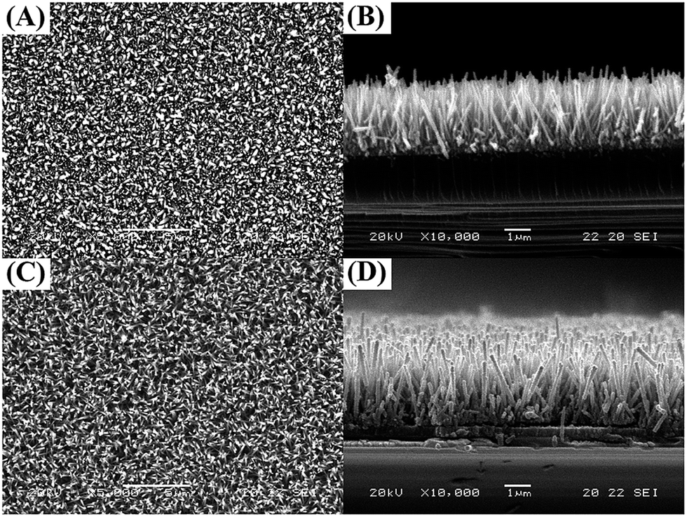 | ||
| Fig. 1 The SEM images of the ZnO NWs array (A) plain view and (B) cross-sectional view; The SEM images of the ZnxCd1−xSe@ZnO core–shell nanocable prepared at 140 °C (C) plain view and (D) cross-sectional view. | ||
Structural characterizations of the samples were performed with XRD, as shown in Fig. 2. An remarkable enhanced ZnO (002) peak with a hexagonal structure was observed for all the samples,29 which indicated the ZnO NWs were grown perpendicular to the FTO substrate with c-axis orientation. All of the peaks were well indexed to the diffraction peaks of ZnO and SnO2. No distinct diffraction peaks related to ZnSe, CdSe, and ZnxCd1−xSe were observed due to the high intensity of the ZnO (002) peaks. However, some weak diffraction peaks related to these materials could be distinguished after the magnification of the XRD spectrum, as shown in insets (1) and (2) of Fig. 2. Two weak diffraction peaks located at 27.5° and 45.5° shown in inset (1) can be indexed to the (111) and (220) planes of cubic ZnSe.30 For the ZnxCd1−xSe/ZnO core–shell NW array prepared at 140 °C, three diffraction peaks located at 25.5°, 42.1°, and 49.9° could be indexed to the (111), (220), and (311) planes of cubic CdSe,7 which are clearly shown in inset (2). The appearance of CdSe diffraction peaks indicated the formation of CdSe shell on the surface of the ZnO NWs. For the ternary ZnxCd1−xSe/ZnO core–shell NW samples, (111) and (220) diffraction peaks of the ZnxCd1−xSe exhibited systematic shift to lower diffraction angles as the reaction temperature increased, as shown in inset (2) of Fig. 2. The peaks shift could be assigned to the lattice constriction effect which originated from more Zn2+ replaced by Cd2+ at a higher reaction temperature. Because the radius of the Cd atoms was larger than that of the Zn atoms, the higher reaction temperature indicated a larger lattice distance.31 According to the Bragg diffraction equation: 2dsinθ = nλ, where d is the lattice distance, θ is the diffraction angle, n is the diffraction order, and λ is the Cu Kα radiation wavelength. The larger lattice distance d led to a shift to lower diffraction angles as observed in inset (2) of Fig. 2.
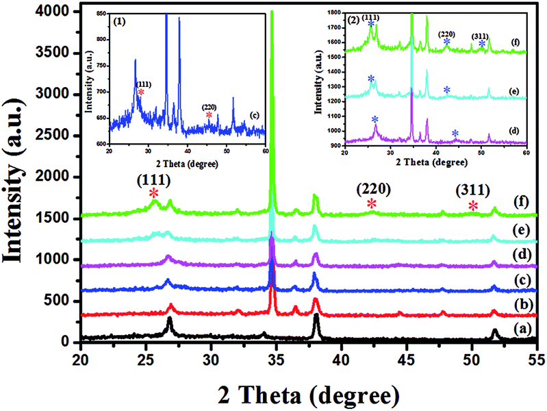 | ||
| Fig. 2 XRD patterns of (a) FTO glass substrate; (b) ZnO NWs; (c) ZnSe/ZnO NWs and (d–f) the ternary core–shell ZnxCd1−xSe/ZnO NWs (0 < x ≤ 1) with different reaction temperature (50 °C, 90 °C, 140 °C). | ||
3.2 Optical absorption and SPS properties
The optical absorption spectra of the samples including the as-prepared ZnO NW array, ZnSe/ZnO NW array, and ZnxCd1−xSe/ZnO core–shell NW array were characterized by UV-Vis spectroscopy, and these spectra are shown in Fig. 3. The pristine ZnO NW array exhibited an absorption edge at approximately 390 nm. In comparison to the pristine ZnO NWs array, the absorption edge of the ZnSe/ZnO NW array shifted to the visible region due to the smaller band gap of ZnSe. Correspondingly, the sample colour changed from white for the pristine ZnO NW array to yellow for the ZnSe/ZnO NW array. For the ZnxCd1−xSe/ZnO core–shell NW array, the band gap gradually decreased as the cation exchange reaction temperature increased, which indicated that the band gap of ZnxCd1−xSe/ZnO core–shell NW array could be continuously tuned from blue to red by controlling the shell composition. The colors of the ZnxCd1−xSe/ZnO core–shell NW array changed from brick red for the sample prepared at 50 °C to dark red for the sample prepared at 140 °C. The photograph images of the ZnSe/ZnO NW array and ZnxCd1−xSe/ZnO core–shell NW array samples are shown in the inset of Fig. 3. | ||
| Fig. 3 The UV-Vis absorption spectra of (a) pristine ZnO NWs array; (b) ZnSe/ZnO NWs array, and (c–e) the ternary core–shell ZnxCd1−xSe/ZnO NWs array (0 < x ≤ 1) at different reaction temperature (50 °C, 90 °C and 140 °C). | ||
To demonstrate the charge separation and transport abilities of the ZnxCd1−xSe/ZnO type II core–shell junction interface, SPS measurements were performed. As a powerful tool to investigate the photo-induced charge separation and transport at interfaces, the SPS technique has been widely employed to obtain the detailed information on photo-induced charge dynamics, including generation, separation and the subsequent transportation.32,33 The SPV measurement system primarily consisted of a monochromatic light source, a lock-in amplifier (SR830-DSP), a sample cell, and the data collection system. A relatively low frequency chopped light of 23 Hz was employed here. Typical SPS spectra are shown in Fig. 4. A sandwich-like structure is adopted for sample measurement, as shown in Fig. 5a. There was a weak SPS response centred at approximately 370 nm for the pristine ZnO NW array, which could be assigned to the band-to-band excitation under light illumination. Because the upper indium tin oxide (ITO) electrode absorbed the light below 370 nm, the SPS response began to decline sharply below 370 nm as observed in Fig. 4. For the ZnSe/ZnO NWs array, the SPS curve could be divided into two photovoltaic response bands. The band at 300–390 nm was attributed to the intrinsic band-to-band excitation of the ZnO core under light irradiation. The second photovoltaic response band ranged from 390 nm to 540 nm. Because no other SPS response was observed in the visible region for the pristine ZnO NW array for its larger band gap (3.37 eV), the second photovoltaic response band could be assigned to the ZnSe shell. The calculated band gap of ZnSe was approximately 2.3 eV according to the SPS threshold value of 540 nm, which was in good agreement with the previously reported band value of ZnSe.22
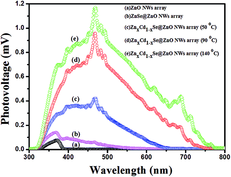 | ||
| Fig. 4 The SPS spectrum of (a) pristine ZnO NWs array; (b) ZnSe@ZnO NWs array, and (c–e) the ternary core–shell ZnxCd1−xSe@ZnO NWs array (0 < x ≤ 1) at different reaction temperature. | ||
 | ||
| Fig. 5 Schematic of (a) the surface photovoltage measurement, and (b) the type II band alignment of ZnxCd1−xSe@ZnO heterojunction and the photo-induced charge separation and transfer process. | ||
For the ZnxCd1−xSe/ZnO core–shell type II samples, two features should be noted as follows: (1) the redshift of the SPS threshold value and (2) enhanced SPS intensity with the increased temperature of cation exchange reaction. It was well known that photovoltage occurs whenever the light-induced charge carriers are separated in space.32 Therefore, the formation of a SPS signal was determined by the fundamental properties of the light absorption as well as the charge separation and transfer. Feature (1) observed in Fig. 4 for the ZnxCd1−xSe/ZnO core–shell type II samples could be attributed to the continuously tuned band gap, which was confirmed by the absorption spectrum. According to the classic SPS theory,32 the enhanced SPS response indicated more photo-induced charge carriers were generated and separated in space. For the ZnxCd1−xSe/ZnO core–shell type II heterojunction, the VBMax and CBMin of the ZnxCd1−xSe shell both lie above those of the ZnO core. The relative band alignments were shown in Fig. 5b. In such a stepwise energy band configuration, the photo-induced electrons could be easily injected from the ZnxCd1−xSe shell into the ZnO core driven by the band alignment. The injected electrons could be swept towards the FTO substrate by the axial internal electric field which had been demonstrated by Zhao et al.33 Such direct and rapid electrons transfer path provided by the ZnO core could substantially decrease the recombination. In addition, the CBMin of the ZnxCd1−xSe shell could be prompt slightly with the increase of Cd2+ at higher cation exchange reaction temperature. The promotion of CBMin led to a higher driving force for the injection of electrons from the ZnxCd1−xSe shell into the ZnO core. Therefore, we observed enhanced SPS intensity with the increased cation exchange reaction temperature as concluded in feature (2).
3.3 Photovoltaic performance of ZnxCd1−xSe@ZnO based solar cells
 | ||
| Fig. 6 Current density–voltage (J–V) characteristics of the solar cells based on the various photoanodes. | ||
| Photoanodes | Voc (mV) | Jsc (mA cm−2) | FF (%) | Efficiency (%) |
|---|---|---|---|---|
| ZnO NW array | 0.07 | 0.18 | 26.82 | No efficiency |
| ZnSe/ZnO NW array | 0.28 | 0.50 | 25.43 | 0.04 |
| ZnxCd1−xSe/ZnO NW array (50 °C) | 0.61 | 3.02 | 49.64 | 0.91 |
| ZnxCd1−xSe/ZnO NW array (90 °C) | 0.59 | 5.56 | 37.85 | 1.25 |
| ZnxCd1−xSe/ZnO NW array (140 °C) | 0.57 | 7.15 | 41.95 | 1.70 |
All of the ZnxCd1−xSe/ZnO based cells exhibited a significant improvement in Jsc and PCE compared to the pristine ZnO and ZnSe/ZnO NW array based cells, which may be due to the following three reasons.12,34 First, the dense ZnxCd1−xSe shell may serve as a passivation layer to protect the ZnO NWs core from etching by the polysulfide electrolyte and inhibit the recombination of injected electrons in the ZnO NW core with the polysulfide electrolyte. Secondly, the better coverage of the ZnxCd1−xSe shell may diminish the number of surface traps on the surface of the ZnO core, which could effectively increase the charge separation ability. More importantly, the photo-induced electrons could easily inject from the ZnxCd1−xSe shell into the ZnO core due to a stepwise energy band configuration. The injected electron could be swept towards the FTO substrate by the axial internal electric field. The direct and rapid electrons transfer path provided by the ZnO NWs core could substantially decrease the recombination, which will effectively improve their photovoltaic performances.
 | ||
| Fig. 7 The SEM images of three kinds of counter electrodes (A) Cu2S, (B) PbS, (C) Cu2ZnSnS4, and (D) the corresponding XRD patterns. | ||
The J–V characteristics of three types of CEs are shown in Fig. 8. The corresponding key photovoltaic parameters obtained from the J–V measurements are summarized in Table 2. The Cu2S, PbS and Cu2ZnSnS4 can be used as CE materials due to their similar p type semiconductor property. X. W. Zeng et al. introduced a Cu2ZnSnSe4 CE to the QDSSCs, which exhibited a better performance than that of thermally platinised conducting glass CEs.37 However, the cell based on our Cu2ZnSnS4 CE exhibited a lowest PCE of 0.99% due to the small FF value, as summarized in Table 2. The lower FF originated from the lower conductivity of Cu2ZnSnS4, which did not facilitate the transport of electrons to the electrode electrolyte interface.38 The planar PbS and nanowalls structured Cu2S CEs exhibited comparable PCEs of 1.62% and 1.70% respectively. There were no significant differences for Voc and FF, as shown in Table 2. However, we should note that the Jsc of the nanowalls structured Cu2S CE (7.15 mA cm−2) was slightly higher than that (6.30 mA cm−2) of the planar PbS CE. The enhanced Jsc may originate from the higher conductivity of Cu2S CE. On the other hand, the large surface area produced by the novel Cu2S nanowall structure could also provide enough reaction sites for the catalytic reduction of Sx2−.36
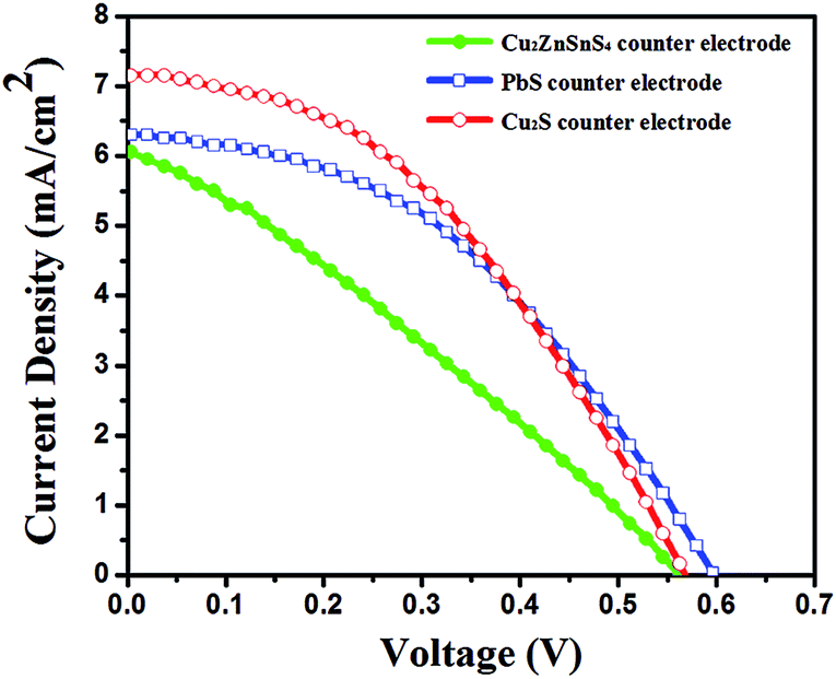 | ||
| Fig. 8 Current density–voltage (J–V) characteristics of the ZnxCd1−xSe@ZnO (140 °C) based solar cells with the various counter electrodes. | ||
| Counter electrodes (CE) | Voc (mV) | Jsc (mA cm−2) | FF (%) | Efficiency (%) |
|---|---|---|---|---|
| Cu2ZnSnS4CE | 0.56 | 6.02 | 29.40 | 0.99 |
| PbS CE | 0.60 | 6.30 | 42.97 | 1.62 |
| Cu2S CE | 0.57 | 7.15 | 41.95 | 1.70 |
4. Conclusions
In summary, highly ordered NW array containing a ZnO core and composition-tunable ZnxCd1−xSe shell was fabricated on the FTO glass substrate. The optical absorption covered nearly the entire visible light region by tuning the shell composition. The SPS measurements indicated that the ZnxCd1−xSe/ZnO core–shell NW array was beneficial for the photo-induced electrons to inject from the ZnxCd1−xSe shell into the ZnO core driven by the band alignment. The catalytic activities of three different CE materials, including Cu2S, PbS, and Cu2ZnSnS4 were investigated based on the ZnxCd1−xSe/ZnO (140 °C)-polysulfide electrolyte system. The Cu2S CE showed a novel nanowall structure with a large surface area, which could provide enough reaction sites for the catalytic reduction of Sx2−. Benefited from the efficient charge separation and transfer ability at the interface of the ZnxCd1−xSe/ZnO core–shell NWs array and the novel Cu2S nanowall CE, the best PCE of 1.70% was obtained. Our results provided the better understanding of the charge separation and transport properties in the type II core–shell heterojunction system.Acknowledgements
This work was supported by Program for Changjiang Scholars and Innovative Research Team in University (no. PCS IRT1126) and the National Natural Science Foundation of China (no. 11274093, 61376061 and 61240053).Notes and references
- D. M. Li, L. Y. Cheng, Y. D. Zhang, Q. X. Zhang, X. M. Huang, Y. H. Luo and Q. B. Meng, Sol. Energy Mater. Sol. Cells, 2014, 120, 454 CrossRef CAS PubMed.
- W. J. Ke, G. J. Fang, H. W. Lei, P. L. Qin, H. Tao, W. Zeng, J. Wang and Z. Z. Zhao, J. Power Sources, 2014, 248, 809 CrossRef CAS PubMed.
- T. Li, Y. Lee and H. Teng, Energy Environ. Sci., 2012, 5, 5315 CAS.
- Z. X. Pan, I. Mora-Sero, Q. Shen, H. Zhang, Y. Li, K. Zhao, J. Wang, X. H. Zhong and J. Bisquert, J. Am. Chem. Soc., 2014, 136, 9203 CrossRef CAS PubMed.
- N. Tétreault and M. Grätzel, Energy Environ. Sci., 2012, 5, 8506 Search PubMed.
- J. Shi, Y. Hara, C. L. Sun, M. A. Anderson and X. D. Wang, Nano Lett., 2011, 11, 3413 CrossRef CAS PubMed.
- J. H. Bang and P. V. Kama, Adv. Funct. Mater., 2010, 20, 1970 CrossRef CAS.
- D. V. Shinde, R. S. Mane, I. Oh, J. K. Lee and S. Han, Dalton Trans., 2012, 41, 10161 RSC.
- T. Rakshit, S. P. Mondal, I. Manna and S. K. Ray, ACS Appl. Mater. Interfaces, 2012, 4, 6085 CAS.
- M. McCune, W. Zhang and Y. L. Deng, Nano Lett., 2012, 12, 3656 CrossRef CAS PubMed.
- K. S. Leschkies, R. Divakar, J. Basu, E. Enache-Pommer, J. E. Boercker, C. B. Carter, U. R. Kortshagen, D. J. Norris and E. S. Aydil, Nano Lett., 2007, 7, 1793 CrossRef CAS PubMed.
- R. Zhang, Q. P. Luo, H. Y. Chen, X. Y. Yu, D. Kuang and C. Su, ChemPhysChem, 2012, 13, 1435 CrossRef CAS PubMed.
- Y. Zhang, T. F. Xie, T. F. Jiang, X. Wei and D. J. Wang, Nanotechnology, 2009, 20, 155707 CrossRef PubMed.
- L. Z. Liu, Y. Q. Chen, T. B. Guo, Y. Q. Zhu, Y. Su, C. Jia, M. Q. Wei and Y. F. Cheng, ACS Appl. Mater. Interfaces, 2012, 2, 17 Search PubMed.
- Z. Z. Lu, J. Xu, X. Xie, H. K. Wang, C. D. Wang, S. Kwok, T. L. Wong, H. L. Kwong, I. Bello, C. Lee, S. Lee and W. J. Zhang, J. Phys. Chem. C, 2012, 116, 2656 CAS.
- Y. Myung, D. M. Jang, T. K. Sung, Y. J. Sohn, G. B. Jung, Y. J. Cho, H. S. Kim and J. Park, ACS Nano, 2010, 4, 3789 CrossRef CAS PubMed.
- Z. X. Wang, X. Y. Zhan, Y. J. Wang, M. Safdar, M. T. Niu, J. P. Zhang, Y. Huang and J. He, Appl. Phys. Lett., 2012, 101, 073105 CrossRef PubMed.
- J. Zhang, X. H. Liu, L. W. Wang, T. L. Yang, X. Z. Guo, S. H. Wu, S. R. Wang and S. M. Zhang, Nanotechnology, 2011, 22, 185501 CrossRef PubMed.
- X. H. Xia, J. P. Tu, Y. Q. Zhang, X. L. Wang, C. D. Gu, X. B. Zhao and H. J. Fan, ACS Nano, 2012, 6, 5531 CrossRef CAS PubMed.
- P. C. Wu, T. Sun, Y. Dai, Y. H. Sun and L. Dai, Cryst. Growth Des., 2011, 11, 1417 CAS.
- Y. J. Hwang, C. Hahn, B. Liu and P. D. Yang, ACS Nano, 2012, 6, 5060 CrossRef CAS PubMed.
- H. X. Li, C. W. Cheng, X. L. Li, J. P. Liu, C. Guan, Y. Y. Tay and H. J. Fan, J. Phys. Chem. C, 2012, 116, 3802 CAS.
- H. Wei, X. L. Ren, Z. Y. Han, T. T. Li, Y. J. Su, L. M. Wei, F. S. Cong and Y. F. Zhang, Mater. Lett., 2013, 102–103, 94 CrossRef CAS PubMed.
- H. Wei, Y. J. Su, Z. Y. Han, T. T. Li, X. L. Ren, Z. Yang, L. M. Wei, F. S. Cong and Y. F. Zhang, Nanotechnology, 2013, 24, 235706 CrossRef PubMed.
- J. Xu, X. Yang, H. K. Wang, X. Chen, C. Y. Luan, Z. X. Xu, Z. Z. Lu, V. A. L. Roy, W. J. Zhang and C. S. Lee, Nano Lett., 2011, 11, 4138 CrossRef CAS PubMed.
- S. A. Vanalakar, R. C. Pawar, M. P. Suryawanshi, S. S. Mali, D. S. Dalavi, A. V. Moholkar, K. U. Sim, Y. B. Kown, J. H. Kim and P. S. Patril, Mater. Lett., 2011, 65, 548 CrossRef CAS PubMed.
- J. Xu, C. Y. Luan, Y. B. Tang, X. Chen, J. A. Zapien, W. J. Zhang, H. L. Kwong, Z. M. Meng, S. T. Lee and C. S. Lee, ACS Nano, 2010, 4, 6064 CrossRef CAS PubMed.
- W. Ki and H. W. Hillhouse, Adv. Energy Mater., 2011, 1, 732 CrossRef CAS.
- K. Cheng, G. Cheng, S. J. Wang, D. W. Fu, B. S. Zou and Z. L. Du, Mater. Chem. Phys., 2010, 124, 1239 CrossRef CAS PubMed.
- S. Bhattacharyya, Y. Estrin, O. Moshe, D. H. Rich and A. Gedanken, ACS Nano, 2009, 3, 1864 CrossRef CAS PubMed.
- S. L. Xie, X. H. Lu, T. Zhai, J. Y. Gan, W. Li, M. Xu, M. H. Yu, Y. M. Zhang and Y. X. Tong, Langmuir, 2012, 28, 10558 CrossRef CAS PubMed.
- L. kronik and Y. Shapira, Surf. Sci. Rep., 1999, 37, 1 CrossRef CAS.
- Q. D. Zhao, M. Yu, T. F. Xie, L. L. Peng and D. J. Wang, Nanotechnology, 2008, 19, 245706 CrossRef PubMed.
- J. Xu, X. Yang, Q. D. Yang, T. L. Wong and C. S. Lee, J. Mater. Chem., 2012, 22, 13374 RSC.
- S. S. Jeon, C. Kim, T. H. Lee, Y. W. Lee, K. Do, J. Ko and S. S. Im, J. Phys. Chem. C, 2012, 116, 22743 CAS.
- Y. Y. Yang, L. F. Zhu, H. C. Sun, X. M. Huang, Y. H. Luo, D. M. Li and Q. B. Meng, ACS Appl. Mater. Interfaces, 2012, 4, 6162 CAS.
- X. W. Zeng, W. J. Zhang, Y. Xie, D. H. Xiong, W. Chen, X. B. Xu, M. K. Wang and Y. B. Cheng, J. Power Sources, 2013, 226, 359 CrossRef CAS PubMed.
- D. Y. Kang, Y. S. Lee, C. Y. Cho and J. H. Moon, Langmuir, 2012, 28, 7033 CrossRef CAS PubMed.
| This journal is © The Royal Society of Chemistry 2015 |