Guosheng Ruana,
Shouliang Wua,
Panpan Wanga,
Jun Liua,
Yunyu Caia,
Zhenfei Tiana,
Yixing Yea,
Changhao Liang*a and
Guosheng Shaob
aKey Laboratory of Materials Physics, Institute of Solid State Physics, Hefei Institutes of Physical Science, Chinese Academy of Sciences, Hefei 230031, China. E-mail: chliang@issp.ac.cn; Fax: +86 551 65591434; Tel: +86 551 65591129
bInstitute for Renewable Energy and Environmental Technologies, University of Bolton, Bolton BL3 5AB, UK
First published on 14th November 2014
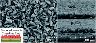
Hematite is an important material used in water splitting and lithium-ion battery electrodes. Electronic conductivity and the visible light-absorption ability of hematite are enhanced by doping impurity ions into the hematite lattice and achieving an appropriate hematite nanostructure. This paper reports the simultaneous doping and growth of tin (Sn)-doped hematite crystalline films on a conducting substrate. The crystalline films were prepared by a hydrothermal process. Laser ablation in liquid induced SnOx colloidal nanoparticles, which were used as the doping source. The obtained compacted films were characterized by scanning electron microscopy, transmission electron microscopy, X-ray diffraction (XRD), X-ray photoelectron spectroscopy, and UV-vis spectrophotometry analyses. XRD results showed the Sn-doped α-Fe2O3 crystalline nanoparticles had dominant active (110) planes. Annealing affected the photoelectrochemical (PEC) performance of the Sn-doped hematite photoanode, and the photocurrent density of the photoanode annealed at 750 °C for 2 h reached the highest value at 0.48 mA cm−2 (at 1.23 V vs. reversible hydrogen electrode). Electrochemical impedance spectroscopy measurements revealed that the charge-transfer resistance of Sn-doped hematite films decreased after the annealing treatment. The improved crystallinity and the preferred (110) plane in the doped crystalline film are favor of the migration of electrons and holes to electrode surfaces, the removal of deleterious surface states and increase of the free electron density, which should contribute to the enhanced PEC performance.
To overcome such disadvantages, several efforts have been made to improve the PEC performance of hematite. These efforts include changing the synthesis method, controlling product morphology, and introducing impurities to increase conductivity among others.13–16 To date, various routes to prepare hematite photoanodes, such as magnetron sputtering,17 sol–gel,18 hydrothermal19 and atmosphere pressure-chemical vapor deposition have been reported.13,20 For significant enhancement in PEC performance, by changing the synthesis method and combined with doping of hetero-atoms is used to adopt.3,8 Hematite is an n-type semiconductor because of the presence of naturally occurring O2 vacancies in its bulk. Tetravalent foreign ions are introduced to substitute trivalent iron ions, forming an n-type doping of hematite. This form is easier to ionize completely, or it forms a covalent bond with O2. Formation of covalent bonds with O2 increases the number of charge carriers and improves electron conductivity. Numerous tetravalent dopants, such as Si,3,21 Ti,20,22,23 Ge,24,25 and Sn26–28 have been introduced in a hematite lattice. Except for key roles of appropriate dopants and structure of hematite, post-thermal treatment of a product is necessary to remove additional organics, decrease interfacial resistance, and increase crystallinity and uniformity of a hematite structure. For instance, Sivula et al.29 reported that thermal treatment of iron oxide (Fe2O3) films at a high temperature (800 °C) induced diffusion of Sn atoms from a transparent fluorine-doped SnO2 (FTO) substrate. This occurrence resulted in increased PEC performance from ca. 10 μA cm−2 to 0.56 mA cm−2 at 1.23 V [vs. reversible hydrogen electrode (RHE)]. Ling et al.13 found that photocurrent densities of Sn-doped hematite nanocorals improved at high annealing temperatures, and highest photocurrent density of 1.86 mA cm−2 at 1.23 V (vs. RHE) was achieved by annealing films at 800 °C for 20 min. Xi et al.30 showed that a specific thermal treatment of iron oxyhydroxides (β-FeOOH) nanorods at 750 °C produced a FexSn1−xO4 layer at the surface, which reduced electron–hole recombination at the hematite–electrolyte interface. Such high annealing temperatures have resulted in damage of the surface layer of a conducting substrate and possible inter-diffusion and reaction between hematite and substrate materials. Thus, the underlying reason for the improvement of PEC performance is still unclear. In this study, a well-grown Sn-doped hematite nanocrystalline film was used to investigate the effects of annealment on the interfacial modification of electrode materials and substrate, migration, possible reaction of dopants and bulk hematite, and the PEC performance of a Sn-doped hematite film. All these parameters were investigated to provide valuable evidence for the practical application of hematite materials in water splitting and lithium-ion electrode.
For PEC measurements, the Sn-doped hematite films were annealed at temperatures that ranged from 0 to 750 °C at a heating rate of 2 °C min−1 held for 2 h. Thereafter, the samples were naturally cooled down to room temperature.
The influence of Sn impurities and annealing temperature on the α-Fe2O3 nanostructure and chemical bonding configuration were investigated. Fig. 2 and 4 show the XRD and XPS measurements of the Sn-doped hematite nanostructures, respectively. As shown in Fig. 2, both the undoped and Sn-doped hematite films display α-Fe2O3 in rhombohedral structure (space group: Rc, JCPDS reference pattern 33-0664). Compared with the standard hematite pattern, the diffraction intensity of (110) plane is stronger than the (104) plane. This suggests that the hematite crystalline preferred growth alone the [110] direction on the substrate and it is desirable because the axis along which the electron mobility is greatest in hematite crystalline.31 Fig. 3a is the TEM image of an individual Sn-doped hematite crystalline, which display the nanopolyhedron appear to be rhombohedral shape with a size about 150 nm. The HRTEM image (Fig. 3b) and corresponding SAED pattern (Fig. 3c) of the boxed area indicate that the lattice fringes fit well to the α-Fe2O3 (110) and (104) planes, the angle between (110) and (104) planes is 56.8°, which is in well fitted with the theoretical data and also our XRD analysis.
![]() | ||
Fig. 3 Sn-doped hematite: (a) low-magnification TEM image, (b and c) HRTEM image and SAED pattern of the boxed area in the edge of crystal. |
![]() | ||
Fig. 4 X-ray photoelectron spectrum of: (a) Fe 2p and (b) Sn 3d obtained from Sn–Fe2O3 thin film sintered at 0 and 750 °C. |
EDX analysis did not produce an accurate calculation of the Sn content in the film because of the influence of Sn atoms present in the FTO substrate. However, XPS with low photoelectron-escape depth (about 5 nm) was able to confirm the concentration of Sn in the resulting films. This process was performed without disturbing the FTO. XPS analyses were performed in the samples with or without annealing at 750 °C. As seen in the high-resolution XPS spectra of Fe 2p (Fig. 4a), the binding energies of Fe 2p1/2 and Fe 2p3/2 appear at 724.5 and 710.9 eV, respectively, with a satellite peak at 719.3 eV. This energy is characteristic of Fe3+ in α-Fe2O3. And in Fig. 4b, there were two peaks centered at 494.6 and 486.2 eV; these peaks corresponded to the Sn 3d3/2 and Sn 3d5/2 binding energy, respectively. The peak at 486.2 eV was caused by SnO2 and a mixture of SnO2 and SnOx (x < 2) because the Sn 3d5/2 binding energy for pure SnO2 was reported as 486.6 eV.32 A doping source produced via LAL is nonstoichiometric SnOx.33 The XPS results showed the same type of SnOx produced. The intensity of the Sn 3d binding energy of the Sn-doped hematite increased after annealing at 750 °C. Similar to XRD analysis, this behavior was caused by a small amount of Sn atoms that precipitated on the surface during high-temperature calcination. These atoms were produced by the doped hematite crystals and FTO layer.34
The UV-vis spectra of the Sn-doped hematite films were also obtained, as shown in Fig. 5a. The transmittance spectra of all the photoelectrodes annealed at different temperatures did not change after thermal treatment. The indirect optical band gaps in Sn-doped hematite were estimated by calculating the intercept of an extrapolated linear fit to the experimental date of a plot of (−lnT)n (T is the transmission value, n = 2 for direct band gap and n = 0.5 for indirect optical band gap) versus the incident photo energy,35 as shown in Fig. 5b. The indirect optical band gap of the Sn-doped film was 2.11 eV. This value coincided with reported values that ranged from 1.9 eV to 2.2 eV. The different values obtained in previous studies were due to differences in preparation method and indirect absorption process of pure-phase hematite.36
![]() | ||
Fig. 5 (a) Transmission spectra of Sn–Fe2O3 films with different thermal treatments and (b) (−ln![]() |
The effect of annealing temperature on the PEC performance of Sn-doped hematite photoanodes was investigated in 1 M of NaOH solution under one sun (AM 1.5 G) irradiation. Dark currents were not detected because they were extremely low. The potential values of the Ag/AgCl used in this study were converted to a RHE scale because photocurrent values in other studies were obtained under standard conditions (1.23 V vs. RHE). This process was performed using the Nernst relationship, as shown below:
ERHE = EAg/AgCl + 0.059pH + E°Ag/AgCl |
The current densities of the as-synthesized and annealed α-Fe2O3 were measured, as shown in Fig. 6. The FTO conductive layer was damaged when the annealing temperature was higher than 750 °C. Therefore, products annealed at temperatures higher than 750 °C were not investigated. The photocurrent densities of the α-Fe2O3 photoelectrodes changed after annealment. The highest photocurrent value was obtained for the film treated at 750 °C for 2 h; its value was 0.48 mA cm−2 at 1.23 V (vs. RHE). The as-deposited α-Fe2O3 exhibited the lowest photocurrent density at 0.02 mA cm−2. Low-temperature annealing produced good crystalline structures and few film defects, thus enhancing the PEC performance. When the annealing temperature was increased up to 600 °C, a decrease in the photocurrent density was observed. This finding was due to increased particle size and precipitation of impurities from the host lattice. Consequently, the amount of recombination center increased. This result was described and partly confirmed in previous studies. The photoelectric properties initially improved and became varied when annealing temperature was increased.37 However, the photocurrent of the as-prepared photoelectrodes in this study was maintained even at increasing annealing temperatures.
![]() | ||
Fig. 6 Photocurrent density of Sn–Fe2O3 photoanodes annealed at different temperatures under one sun (AM 1.5 G) illumination in 1 M of NaOH electrolyte solution. |
Electrochemical impedance spectroscopy (EIS) measurements were performed to obtain further evidence of the influence of annealing temperature on the PEC performance of hematite photoanodes. Measurements were performed under the same condition of gas evolution (at 1.23 V vs. RHE, 1 M of NaOH solution) under one sun irradiation. Fig. 7 shows the Nyquist plots of the photoanodes annealed at different temperatures, where the points were measured values and the solid curves were fitted results of an equivalent RC-circuit model (inset). The values of the elements obtained by fitting results are presented in Table 1. This table contains data on charge-transfer resistance (R) across the interfaces in the photoanode and constant phase elements (CPE) in parallel. The dates for all photoanodes fitted well with the two-RC circuit model but not with the classic three-RC circuit model for pure hematite films. Previous studies showed that three-RC circuits were assigned to Fe2O3∥electrolyte (R3), Fe2O3 film (R2), and Fe2O3∥FTO (R1), respectively.38,39 Since the electrode film were grown in situ in a hydrothermal process and the interface resistance of Fe2O3∥FTO was very small and negligible. R1 is not considered here in calculation.
![]() | ||
Fig. 7 Nyquist plots of Sn–Fe2O3 photoanodes. Points are measured values and solid curves are fitted lines. The inset shows the equivalent circuit. |
(R/ohm) (CPE/F) | Rs | R1 CPE1 | R2 CPE2 | R3 CPE3 |
---|---|---|---|---|
0 °C | 21.33 | 9463 3.11 × 10⁻⁶ | 71![]() |
|
450 °C | 12.88 | 8333 1.48 × 10⁻⁶ | 11![]() |
|
550 °C | 9.28 | 5376 1.82 × 10⁻⁷ | 9522 3.75 × 10⁻⁶ | |
650 °C | 11.11 | 290.6 2.73 × 10⁻⁸ | 5641 1.07 × 10⁻⁷ | |
750 °C | 21.91 | 86.84 1.46 × 10⁻⁶ | 5248 1.10 × 10⁻⁶ |
RS is the sheet resistance in a half-cell test system for EIS. The obtained Rs values were similar because of the same test conditions employed. However, the values for R2 and R3 changed significantly. The R2 originated from the charge distribution among doped-Fe2O3 crystals. Table 1 shows that R2 decrease sharply as the annealing temperature increased. The Mott–Schottky curves (Fig. S2†) also show that the slope of photoanode is reduced after thermal treatment, reflecting the significantly increase of carrier concentration. High concentration free electrons indicate the rapid and efficient separation of the photo-generated carrier. R3/CPE3, the largest semicircle corresponds to Fe2O3∥electrolyte interface in the PEC systems, is closely related to the holes transfer. The holes generated by photo-excitation are transmitted to the anode surface, and O2 can be produced during water splitting. As the Table 1 showing, R3 also decreased with annealing temperature increasing. R3 of the Sn-doped hematite photoanode annealed at 750 °C decreased by more than 100 times compared with that of the untreated hematite photoanodes. Here, the improved crystallinity after annealing treatment and the preferred (110) plane in the doped crystalline film are favor for the migration of electrons and holes to electrode surfaces, which should be main contributions to the significantly decrease of R2 and R3 and enhanced PEC performance. Moreover, Hamann et al.40 demonstrated that annealing at elevated temperature can further remove the deleterious surface states of hematite. Ling et al.,13 also proposed that Sn-doping improves the free electron density of hematite.
Footnote |
† Electronic supplementary information (ESI) available. See DOI: 10.1039/c4ra13124j |
This journal is © The Royal Society of Chemistry 2014 |