From two-dimensional to one-dimensional structures: SiC nano-whiskers derived from graphene via a catalyst-free carbothermal reaction

Zhuo Liua, Qing-Qiang Konga, Cheng-Meng Chen*a, Qiang Zhangb, Ling Hub, Xiao-Ming Lia, Pei-De Hanc and Rong Caiad
aInstitute of Coal Chemistry, Chinese Academy of Sciences, Taiyuan 030001, P. R. China. E-mail: ccm@sxicc.ac.cn
bDepartment of Chemical Engineering, Tsinghua University, Beijing 100084, P. R. China
cCollege of Materials Science and Engineering, Taiyuan University of Technology, Taiyuan 030024, P. R. China
dAcademy of Opto-Electronics, Chinese Academy of Sciences, Beijing 100094, P. R. China

Received 28th September 2014 , Accepted 9th December 2014

First published on 9th December 2014


Abstract

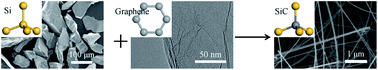
One-dimensional β-SiC nano-whiskers are synthesized from two-dimensional graphene by a facile catalyst-free carbothermal reaction. Comparing with closed or semi-closed carbon sources, the large exterior surface area and exposed rich edge render graphene an ideal carbon source for the scale-up production of carbide materials.


As a highly orientated single crystal fiber with diameters from nano- to micro-scale, SiC whiskers (SiCws) have similar cubic lattices to diamonds. They ranks superior to other one-dimensional (1D) nanostructures in terms of their excellent mechanical stiffness and high resistance to heat, abrasion, oxidation, thermal shock and erosion.1 For example, β-SiC has a Mohs’ hardness scale of 9.50, a tensile strength of 101 GPa, a Young’s modulus of 558 GPa, and a fusing point of over 2700 °C.2 Consequently, SiCws have been widely employed as reinforcing fillers or coating materials for plastics, metals or ceramic based composites towards applications in cutting tools, microwave-heating inserts and aeroengines etc.1,3–5 To fabricate the SiCws, a carbothermal reaction of a silicon source such as nano-silicon powder or dimethylsilane with a carbon source at a temperature ranging from 1400 to 1800 °C is usually used. Various carbon derivatives have been employed as the carbon source for the SiCws, including graphite powder,6,7 activated carbon,8 carbon fibers,9 carbon black,10 carbon nanotubes (CNTs),11 biomass carbon,12 etc. The morphology of SiCws strongly depends on the selection of the carbon source. Increasing the specific surface area was a good choice to obtain high quality and low diameter whiskers.13 As already commercialized in the US and Japan, a carbothermal reaction with biomass carbon such as rice husks was adapted for the scale-up production of SiCws, due to the natural combination of carbon and silicon sources in the cell wall.12,14 However, the quality of the SiC whiskers derived from biomass should be further improved to avoid the formation of SiC particulates with large diameters, uncontrollable quality, low yield, and complex pretreatment of biomass.

As the two-dimensional (2D) crystal of sp2 conjugated carbon atoms, graphene possesses rich edges, a high theoretical surface area (2630 m2 g−1), and low bulk density,15 which renders it a promising candidate to replace the cellular network as the carbon source for SiCws. Benefiting from the sheer openness of the surface, as well as the chemically active dangling bonds at the edges and defective sites, graphene provides abundant attacking points in a Si-containing atmosphere, which facilitates the combination of C and Si even through a one step reaction without a catalyst. Since the scale-up amount of graphene can be facilely produced by the thermal exfoliation of graphite oxide with natural graphite as the raw material,16,17 it has become a highly accessible and cost effective precursor for SiCws.

Herein, the synthesis of SiC nano-whiskers was explored with thermally reduced graphene (TRG) as the novel 2D carbon source without any assistance from a catalyst. TRG was obtained by thermal exfoliation and carbonization of graphite oxide from a modified Hummers method.18,19 Interestingly, it is well known that graphene can be prepared by epitaxial growth from the basal plane surface of SiC,20–22 while an inverse process has not yet been reported. The thermochemistry and growth mechanism of SiC crystals of the whiskers are proposed in this report. This work paves a new pathway for the fabrication of 1D carbide nanostructures from 2D graphene sheets.

As shown in Fig. 1a, the fluffy black powder of TRG was employed as the carbon source, and the carbothermal reaction between the graphene and silicon powders (Fig. S1, commercially available, 200 meshes with a purity of 99.9%) was carried out at 1600 °C. Afterwards, the as-obtained material was purified by removing any residual precursors of the unreacted carbon and silicon. The as-obtained material became celadon. X-ray diffraction (XRD) characterization was employed to confirm the formation of SiC, as shown in Fig. 1b. The diffraction peaks were assigned to be pure β-SiC growing in a (111) direction. Compared with the standard peak pattern (JCPDS 29-1129), an additional peak at 2θ ≈ 33.81° was observed. It is attributed to the stacking faults, which are widely detected in β-SiC due to its low formation energy.23,24 Fig. 1c shows the Fourier transformation infrared spectrum (FT-IR) of the sample. The absorption peak at 813 cm−1 was attributed to the Si–C stretching vibration, while the broad and weak absorption peaks at 400–500 cm−1 and 1000–1300 cm−1 were assigned to the Si–O stretching vibrations.9,12 The presence of O was also confirmed by EDX equipped on scanning electron microscopy (SEM). Therefore, the as-obtained sample consisted of mainly SiC with a minor amount of silicon oxides, which was derived from the residual oxygen in the precursors.


image file: c4ra11380b-f1.tif
Fig. 1 The synthetic procedure and structural characterizations of SiC nano-whiskers. (a) A schematic view of the catalyst-free carbothermal reaction, (b) the XRD pattern and (c) the FT-IR spectrum of the as-obtained SiC nano-whiskers.

The morphologies of the graphene precursor, intermediate products and resulting SiCws were characterized by SEM and transmission electron microscopy (TEM) (Fig. 2). As the carbon source, the fluffy TRG facilitated the diffusion of silicon vapor and the intimate contact with carbon atoms in the graphene lattice due to its opened macroporous structure (Fig. 2a) and high specific surface area (434.1 m2 g−1 by the Brunauer–Emmett–Teller method,25 BET) (Fig. 2b). Besides, the liquid-phase oxidation and thermal decomposition process preserved the 2D graphene lattice with topological defects, atomic vacancies, dangling bonds, and a trace amount of thermally stable oxygen functionalities,16,25 which served as the reactive sites for the initial nucleation of SiC. It is noteworthy that, comparing with the defects inside the basal plane, the edges were more inclined to work as the energetically favored sites for the adsorption of silicon vapor, forming a metastable SiC nucleus. Fig. 2c shows the intermediate products without the removal of the residual carbon and silicon sources. The initial formation of amorphous SiC seeds began at the edge of the graphene sheet, and then the corrosion proceeded towards the central part. Fig. 2d–f display the final morphology of SiC nano-whiskers with diameters of 30–80 nm and lengths of more than 10 μm. The products exhibited a specific surface area of 11.6 m2 g−1, corresponding to an average diameter of 60.6 nm for the fiber-type SiC materials roughly calculated based on a column model (Fig. S2). In addition, a trace amount of spherical particles also coexisted.


image file: c4ra11380b-f2.tif
Fig. 2 Morphology characterizations of the precursor, intermediate, and final product. (a and b) SEM and TEM images of TRG at 1000 °C, working as the carbon source; (c) the intermediate product without removal of the residual graphene and silicon; (d and e) the as-obtained SiC nano-whiskers at low and high magnifications; (f) a histogram of the diameter distributions of the SiC nano-whiskers.

TEM was employed to obtain further information on the crystal structure. Most of the whiskers had continuously changing diameters with a periodicity of every 55–70 nm (Fig. 3), and a small ratio of nanowires had relatively stable diameters (Fig. S3) or bamboo-like structures (Fig. S4). The interplanar spacing was calculated to be 0.254 nm from Fig. 3d, corresponding to the (111) plane of β-SiC. Crystal defects, such as stacking faults (arrow A) and nanotwins (arrow B) were observed, which altered the stacking sequence of the (111) planes to yield an additional peak at 2θ ≈ 33.81° (Fig. 1b). The coexistence of stacking faults and nanotwins contributed to the increased hardness and fracture toughness, as well as oxidation resistance by generating internal stress.26 Moreover, the selected area electron diffraction (SAED) pattern in Fig. 3b was distributed separately and uniformly, corresponding to good crystallinity. Therefore, the as-obtained β-SiC whiskers were mostly grown in the direction of (111), and the stacking faults mainly appeared in the regions of the whiskers with varied diameters. As shown in Fig. 3c, a stacking fault just occurred in the neck region with a smaller diameter, and the diameter increased again after meeting the stacking fault. The continuously changing diameter in the well-defined single crystal sections was due to the tendency to develop (111) type side surfaces.10 Therefore, it was deduced that the microscopically rough surface resulted from the stacking faults.


image file: c4ra11380b-f3.tif
Fig. 3 (a) TEM image of the SiC nano-whiskers with continually changing diameters; (b) SAED and (c and d) HRTEM images of the SiC whiskers observed in (a). Stacking faults and nanotwins are marked with red arrows A and B, respectively.

As the whole carbothermal reaction was accomplished in an insert Ar atmosphere without the assistance of a catalyst, the formation of the SiCws was described as the decomposition and recombination of silicon with a carbon precursor at a high temperature, as shown in eqn (1):

 
Si + C → SiC (1)

The growth mechanism of the SiCws is suggested in Fig. 4. Firstly, the melting silicon partially changes into a vapor phase at 1600 °C, which is then diffused and physically adsorbed onto the surface of the 2D graphene crystal (Fig. 4a). Secondly, the Si–C bonds start to form between the silicon and carbon atoms with a simultaneous breaking of C–C bonds. It is noteworthy that the carbons at the edges and topological defects, with unsaturated dangling bonds and radicals, are more reactive than the carbons in the intact sp2 basal plane (Fig. 4b).6,13 Therefore, the nucleation of the SiC seeds are initially formed at the edge of the graphene, which is then developed in-plane towards the central part of the graphene (Fig. 4c). Finally, when the SiC seeds grow to a certain scale (ca. 30–80 nm, which is roughly equal to the maximum diameter of the final SiCw), it will break away from the graphene substrate. Afterwards, the newly formed individual SiC seeds will merge at the driving force of 1D growth habit along the (111) plane of β-SiC, pushing the further prolongation of the whiskers from the root. At the same time, recrystallization may also take place in the formed whiskers to increase the crystallinity (Fig. 4d). Generally, the growth progress was suggested to be a continuous corrosion-merger process from the edge to the basal plane of graphene: first, the graphene edge was ‘corroded’ by silicon vapor due to the unsaturated dangling bonds and radicals. Nucleation of SiC seeds formed at the edge of graphene, and proceeded towards the central part. Second, the SiC seeds break away from the graphene substrate, and ‘merged’ at the driving force of decreasing surface energy. It is quite similar to the growth pattern of other related nano-materials, such as the growth of CNT multilayers.27 In this process, two key features of the carbon source are essential for the successful synthesis of high quality SiCws: (a) the low dimensional structure with highly accessible surface area for physical diffusion, (b) exposed rich edges and defects in the carbon lattice to facilitate the nucleation and detachment of the SiC seeds. Among all the carbon allotropes, 2D graphene is the ideal carbon to meet the above requirements.


image file: c4ra11380b-f4.tif
Fig. 4 Growth mechanism of the SiCws. (a) The silicon precursor changed from a crystal to a vapor; (b) the silicon vapor diffused and combined with graphene; (c) SiC crystal seeds formed and then breakaway from the edge; (d) SiC seeds merged and recrystallized into the 1D whisker. Si and C atoms are represented by yellow and gray balls, respectively.

In order to verify the edge effects of the carbon source, several control samples were employed under the same carbothermal conditions. As shown in Fig. 5a, the multi-walled CNTs were a semi-closed structure with opened edges at both ends.28 When it was used as the carbon source (Fig. 5b), only short and curled SiC fibers were obtained, which maintained the original morphology of the CNTs, in accordance with the shape memory synthesis of SiC from CNTs.11,29 Moreover a carbonaceous aerogel, constructed by edge-to-edge assembly of graphene sheets, was fabricated and employed (Fig. 5c). In this architecture, the exposed graphene edges have been sealed by the cross-linkage with each other.30 As shown in Fig. 5d, after the reaction, no whiskers were formed, and the aerogel collapsed and corroded by forming nanoparticle assembled sheets. Though the 3D inter-connected opened surface facilitated the mass diffusion and complete combination of silicon and carbon, the breakaway of the SiC seeds was retarded due to the higher energy consumption from the internal region of the graphene. Therefore, SiC crystal seeds can be formed in a substrate of CNTs and graphene aerogel, but the breakaway and secondary assembly of whiskers were inhibited due to the semi-closed or closed edges.


image file: c4ra11380b-f5.tif
Fig. 5 The SEM images of the controlled experiments with different carbon sources. (a and b) Multi-walled CNTs and the corresponding SiC product; (c and d) carbonaceous aerogel and the corresponding SiC product; (e and f) expanded graphite and the corresponding SiC product; (g and h) graphite and the corresponding SiC product. The insets in (a), (c), (e) and (g) display the models of the carbon sources with reactive sites being indicated by the yellow regions.

In order to verify the influence of the dimension (thickness or stacking degree) and surface openness of a carbon precursor on the resulting SiCws, expanded graphite (Fig. 5e) and graphite powders (Fig. 5g) were also used as the carbon sources. Fig. 5f displays the final morphology of the product with expanded graphite working as the carbon source. SiC nanoparticles agglomerated into a sheet in a skeleton shape, and several whiskers were observed simultaneously. Partial exfoliation from the natural flake graphite increased the distance between the graphene layers, but the distance was not large enough for further growth of the SiCws. Fig. 5h displays the morphology of SiC with graphite as the carbon source. The nanoparticles of SiC accumulated on the surface of the graphite particles. The cross section was also covered by the SiC nanoparticles, maintaining the layered structure of graphite. The closely packed graphite flake prevented further diffusion of Si vapor, resulting in only a small amount of SiCws. These whiskers were synthesized from the occasional exfoliated graphite flake. The XRD patterns of the final products derived from the above carbon sources are given in Fig. S5. Similar experiments have been designed with open, semi-closed, and closed carbon systems for the liquid phase oxidation and exfoliation of carbon precursors for graphene.28

Conclusions

In summary, 1D β-SiC nano-whiskers with a diameter of 30–80 nm and a length of more than 10 μm were synthesized with 2D graphene as the carbon source as well as the active substrate for the first time. The large exterior surface and abundant opened edges were the key factors for the synthesis of high quality whiskers. The former facilitated the transmission and in situ deposition of Si vapor, as well as the combination with C, while the latter decreased the energy barrier for the breakaway of SiC crystal seeds, and re-assembly and re-crystallization took place after the breakaway. The growth was completed by a corrosion-merger process during the catalyst-free carbothermal reaction. As a novel 2D crystal, graphene has been proved to be an ideal carbon source for the synthesis of high quality SiCws, and this research also provides a simplified model for investigating the formation mechanism of these 1D structures during carbothermal reactions between carbon and silicon.

Acknowledgements

The authors thank the financial support from the Innovative Research Fund of ICC-CAS (2012SCXQT03), Natural Science Foundation of China (51302281), Natural Science Foundation of Shanxi Province (2013011012-7), Innovative Research Fund of Taiyuan Science and Technology Bureau (2012CXJD0510), Shanxi Coal Transportation and Sales Group Co. Ltd (2013WT103).

Notes and references

  1. G. Rosario, Properties and Applications of Silicon Carbide, InTech, Croatia, 2011, pp. 197–198 Search PubMed .
  2. W. X. Li and T. Wang, Phys. Rev. B: Condens. Matter, 1999, 59, 3993 CrossRef CAS .
  3. A. R. Thangaraj and K. J. Weinmann, J. Manuf. Sci. Eng., 1992, 114, 301 CrossRef .
  4. P. H. McCluskey, P. K. Williams, R. S. Graves and T. N. Tiegs, J. Am. Ceram. Soc., 1990, 73, 461 CrossRef CAS PubMed .
  5. S. H. N. Doo, W. B. Lim, J. S. Lee, C. S. Han and Y. S. Cho, Int. J. Appl. Ceram. Technol., 2014, 11, 240 CrossRef CAS PubMed .
  6. K. Chen, Z. H. Huang, J. T. Huang, M. H. Fang, Y. G. Liu, H. P. Ji and L. Yin, Ceram. Int., 2013, 39, 1957 CrossRef CAS PubMed .
  7. T. Seeger, P. Kohler-Redlich and M. Rühle, Adv. Mater., 2000, 12, 279 CrossRef CAS .
  8. J. L. Kuang and W. B. Cao, J. Am. Ceram. Soc., 2013, 96, 2877 CrossRef CAS PubMed .
  9. Z. Y. Ryu, J. T. Zheng, M. Z. Wang and B. J. Zhang, Carbon, 2001, 39, 1929 CrossRef CAS .
  10. L. Wang and H. Wada, J. Mater. Res., 1992, 7, 148 CrossRef CAS .
  11. Z. Pan, H. L. Lai, F. C. K. Au, X. Duan, W. Zhou, W. Shi, N. Wang, C. S. Li, N. B. Wong, S. T. Lee and S. Xie, Adv. Mater., 2000, 12, 1186 CrossRef CAS .
  12. C. B. Raju and S. Verma, Br. Ceram. Trans., 1997, 96, 112 CAS .
  13. R. B. Wu, G. Y. Yang, Y. Pan, L. L. Wu, J. J. Chen, M. X. Gao, R. Zhai and J. Lin, Appl. Phys. A: Mater. Sci. Process., 2007, 88, 679 CrossRef CAS PubMed .
  14. Y. L. Chiew and K. Y. Cheong, Mater. Sci. Eng., B, 2011, 176, 951 CrossRef CAS PubMed .
  15. V. Chabot, D. Higgins, A. P. Yu, X. C. Xiao, Z. W. Chen and J. J. Zhang, Energy Environ. Sci., 2014, 7, 1564 CAS .
  16. B. Akbar, M. Cecilia, A. Muge, J. C. Yves, C. Manish and B. S. Vivek, Nat. Chem., 2010, 2, 581 CrossRef PubMed .
  17. K. R. Paton, E. Varrla, C. Backes, R. J. Smith, U. Khan, A. O’Neill, C. Boland, M. Lotya, O. M. Istrate, P. King, T. Higgins, S. Barwich, P. May, P. Puczkarski, I. Ahmed, M. Moebius, H. Pettersson, E. Lomg, J. Coelho, S. E. O’Brien, E. K. McGuire, B. M. Sanchez, G. S. Duesberg, N. McEvoy, T. J. Pennycook, C. Downing, A. Croosley, V. Nicolosi and J. N. Coleman, Nat. Mater., 2014, 13, 624 CrossRef CAS PubMed .
  18. W. S. Hummers and R. E. Offeman, J. Am. Chem. Soc., 1958, 80, 1339 CrossRef CAS .
  19. W. Lv, D. M. Tang, Y. B. He, C. H. You, Z. Q. Shi, X. C. Chen, C. M. Chen, P. X. Hou, C. Liu and Q. H. Yang, ACS Nano, 2009, 3, 3730 CrossRef CAS PubMed .
  20. E. Rollings, G. H. Gweon, S. Y. Zhou, B. S. Mun, J. L. McChesney, B. S. Hussain, A. V. Fedorov, P. N. First, W. A. de Heer and A. Lanzara, J. Phys. Chem. Solids, 2006, 67, 2172 CrossRef CAS PubMed .
  21. S. Y. Zhou, G. H. Gweon, A. V. Fedorov, P. N. First, W. A. Heer, D. H. Lee, F. Guinea, A. H. C. Neto and A. Lanzara, Nat. Mater., 2007, 6, 770 CrossRef CAS PubMed .
  22. J. Robinson, X. J. Weng, K. Trumbull, R. Cavalero, M. Wetherington, E. Frantz, M. LaBella, Z. Hughes, M. Fanton and D. Snyder, ACS Nano, 2010, 4, 153 CrossRef CAS PubMed .
  23. V. P. Vijay and D. C. James, J. Am. Ceram. Soc., 1995, 78, 774 CrossRef PubMed .
  24. A. Chrysanthou and P. Grieveson, J. Mater. Sci., 1991, 26, 3463 CrossRef CAS .
  25. C. M. Chen, Q. Zhang, M. G. Yang, C. H. Huang, Y. G. Yang and M. Z. Wang, Carbon, 2012, 50, 3572 CrossRef CAS PubMed .
  26. Q. Huang, D. L. Yu, B. Xu, W. T. Hu, Y. M. Ma, Y. B. Wang, Z. S. Zhao, B. Wen, J. L. He, Z. Y. Liu and Y. J. Tian, Nature, 2014, 510, 250 CrossRef CAS PubMed .
  27. X. S. Li, A. Y. Cao, Y. J. Jung, R. Vajtai and P. M. Ajayan, Nano Lett., 2005, 5, 1997 CrossRef CAS PubMed .
  28. S. Zhang, L. X. Zhu, H. H. Song, X. H. Chen, B. Wu, J. S. Zhou and F. Wang, J. Mater. Chem., 2012, 22, 22150 RSC .
  29. C. C. Tang, S. S. Fan, H. Y. Dang, J. H. Zhao, C. Zhang, P. Li and Q. Gu, J. Cryst. Growth, 2000, 210, 595 CrossRef CAS .
  30. H. Huang, P. W. Chen, X. T. Zhang, Y. Lu and W. C. Zhan, Small, 2013, 9, 1397 CrossRef CAS PubMed .

Footnote

Electronic supplementary information (ESI) available: Experimental details, characterization and control experimental details. See DOI: 10.1039/c4ra11380b

This journal is © The Royal Society of Chemistry 2015