DOI:
10.1039/C4RA11305E
(Paper)
RSC Adv., 2014,
4, 53999-54006
Noncovalently grafting sulfonic acid onto graphene oxide for improved hole transport in polymer solar cells†
Received
26th September 2014
, Accepted 9th October 2014
First published on 10th October 2014
Abstract
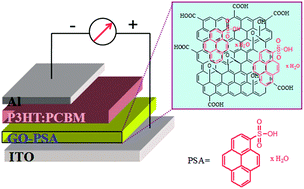
Sulfonic acid was successfully grafted onto graphene oxide (GO) via a facile noncovalent functionalization approach using pyrene as the anchoring bridge, affording a novel water-processable sulfonic acid functionalized GO, which shows improved hole transport in polymer solar cells (PSCs) compared to that of pristine GO. The successful grafting of 1-pyrenesulfonic acid (PSA) onto the carbon basal plane of GO is confirmed by FT-IR, UV-vis and Raman spectroscopic studies. An AFM study on the film morphology of GO–PSA reveals that the PSA moiety attaches onto both sides of the single layered graphene sheets, thus prohibiting the exfoliated single-layer graphene sheets from re-stacking. Finally, GO–PSA was applied as an effective hole transport layer (HTL) in poly(3-hexylthiophene-2,5-diyl):[6,6]-phenyl-C61-butyric acid methyl ester (P3HT:PCBM) bulk heterojunction (BHJ) PSC devices. Under the optimized conditions, the ITO/GO–PSA/P3HT:PCBM/Al BHJ-PSC device has a power conversion efficiency (PCE) of 2.86%, which is enhanced by ca. 42.3% compared to that of the reference device based on pristine GO HTL (2.01%). The PCE enhancement is primarily attributed to the increase of fill factor (FF) due to the improved hole transport of GO upon PSA grafting, which results from the improved conductivity of GO upon PSA grafting and the decrease of the contact resistance between P3HT and GO because of the enhanced surface doping of P3HT by the –OSO3H groups.
1. Introduction
The single graphene sheet, a two-dimensional material composed of sp2-hybridized carbon atoms, has been drawing great attention since its discovery by Geim and coworkers in 2004.1 Due to its peculiar properties such as high carrier mobility (2 × 105 cm2 V−1 s−1), good optical transparency (∼97.7%), high thermal conductivity (∼5 × 10³ Wm−1 K−1 at room temperature), large theoretical surface area (2630 m2 g−1) and high breaking strength (42 N m−1),2,3 graphene has been widely applied in a variety of devices including organic photovoltaics (OPVs),3–14 organic light-emitting diodes (OLEDs),15 field-effect transistors,16 and supercapacitors.17 In particular, graphene and its derivatives have been reported to be intriguing candidates for bulk heterojunction (BHJ) polymer solar cells (PSCs) as electrode materials,4 acceptors in photoactive layers5–9 or interfacial layer materials.10–14 While the pristine graphene was primarily used as a transparent electrode material substituting the commonly used indium tin oxide (ITO) electrode because of its excellent conductivity, good flexibility and transparency, it suffers from poor dispersity in common organic solvents which is a prerequisite for film fabrication of both photoactive and interfacial layers.18–21 Hence, functionalization of graphene appears crucial for application of graphenes in PSCs. Among them, graphene oxide (GO), a functionalized graphene with hydroxy and epoxy groups attached on the basal plane and carboxyl groups linked at the edges,13,22 has been extensively studied as an alternative hole transport layer (HTL) with the function of selectively transporting holes and blocking electrons, and GO HTL-incorporated BHJ-PSC device based on poly(3-hexylthiophene-2,5-diyl):[6,6]-phenyl-C61-butyric acid methyl ester (P3HT:PCBM) shows a relatively high power conversion efficiency (PCE) of 3.5%.14
Due to the attachments of hydrophilic hydroxy and carboxyl groups onto the hydrophobic carbon basal plane, GO is amphiphobic and the electrical conductivity of GO is dramatically lower than that of the pristine graphene because the covalent C–O bonds damage the large-scale π–π conjugation within the hexagonal carbon lattices.23 Thus, it is highly desirable to functionalize GO so as to enhance its conductivity, and consequently to apply the functionalized GO as HTL in PSCs substituting the commonly used HTL, poly(3,4-ethylenedioxythiophene):poly(styrene sulfonate) (PEDOT:PSS), which is acidic and hygroscopic and might damage the ITO electrode.24 So far a few covalent and noncovalent approaches have been established to synthesize functionalized GO.6,13,25–27 For instance, Jen et al. deposited a thin layer of GO on top of P3HT film, increasing dramatically the conductivity of P3HT by six orders of magnitude, and the conductivity enhancement was interpreted by the protonic doping of P3HT by GO.6 Dai et al. synthesized the first sulfated GO (GO–OSO3H) in which –OSO3H groups was attached to the carbon basal plane of GO via C–O covalent bonds. The resultant GO–OSO3H exhibited much higher conductivity compared to the pristine GO, and incorporation of GO–OSO3H as HTL in P3HT:PCBM BHJ-PSC devices led to obviously enhanced PCE. The PCE enhancement was explained by not only the well-matching of the work function between GO–OSO3H and P3HT but also the interfacial doping of P3HT by GO–OSO3H.13 On the other hand, GO derivatives with appropriate functionalization can be used as electron extraction layer as reported in two studies.27,28 Dai et al. synthesized a cesium-neutralized GO (GO-Cs) via a simple charge neutralization of the periphery –COOH groups of GO with Cs2CO3, which showed excellent electron extraction in P3HT:PCBM BHJ-PSC devices.28 Very recently we synthesized a graphene–fullerene composite by noncovalently attaching PCBM onto reduced GO, which behaved as an efficient electron extraction layer in P3HT:PCBM BHJ-PSC devices.27 These studies indicate that functionalization of GO should be carefully controlled in order to retain the commonly demonstrated hole transport property of GO.
Herein, we report the synthesis of a new sulfonic acid functionalized GO (GO–PSA) via a facile noncovalent functionalization approach, in which sulfonic acid was successfully grafted onto GO with pyrene as the anchoring bridging. The as-synthesized GO–PSA was successfully applied as HTL in P3HT:PCBM BHJ-PSCs, showing improved hole transport compared to the pristine GO.
2. Experimental
2.1. Materials
Poly(3-hexylthiophene) (P3HT) and [6,6]-phenyl-C61-butyric acid methyl ester (PCBM) were purchased from Luminescence Technology Corp. and Nichem Fine Technology Co., Ltd, respectively. 1-Pyrenesulfonic acid (PSA) and nano graphite powder were bought from Aldrich and Aladdin, respectively. K2S2O8, KMnO4, P2O5 and H2O2 were purchased from Sinopharm Chemical Reagent Co. Ltd., China. All materials were used as received without further treatment.
2.2. Characterization
FT-IR spectra were measured on a TENSOR 27 spectrometer (Bruker, Germany) by mixing samples with KBr pellet at room temperature. UV-vis absorption spectra were recorded on a UV-3600 spectrometer (Shimadzu, Japan) using a quartz cell of 10 mm layer thickness and 1 nm resolution. Raman spectra were carried out at room temperature with a LABRAM-HR equipment (JobinYvon, France) processed at a wavelength of 514.5 nm as the excitation source, and the samples were dropped onto silicon substrates and dried into a film. The morphology of sample was studied by AFM (Nanoscope III, Digital Instruments, USA).
2.3. Synthesis
The synthetic route of GO–PSA is shown in Scheme 1. The detailed synthetic procedures are as follow:
 |
| Scheme 1 The synthetic route of GO–PSA. | |
Preparation of GO. GO was synthesized from nano graphite powder via Hummers' method as reported in literatures.29,30 In brief, nano graphite powder was oxidized through two steps to obtain GO. First, 0.6 g nano graphite powder, 4.8 mL concentrated H2SO4, 1.0 g K2S2O8 and 1.0 g P2O5 were mixed in a 100 mL flask and heated at 80 °C for 4.5 h. Then the vacuum filtration was carried out to get the residue, which was washed by excess deionized (DI) water and then dried at 60 °C in vacuum. 3.0 g KMnO4 was then added slowly into the pre-oxidized graphite in 24 mL concentrated H2SO4 under ice-water bath. The mixture turned into dark green and heated at 35 °C for 2 h. 50 mL DI water was added into the mixture, which was heated for another 2 h at the same temperature with the colour turning into dark gradually. Finally, 140 mL DI water and 4 mL 30% H2O2 were added. The colour changed to bright yellow. The mixture containing GO was filtrated immediately. The residue was washed by 100 mL HCl solution and 70 mL DI water and dispersed in DI water, followed by ultrasonication until the brown viscous solid disappeared.
Synthesis of GO–PSA. First, GO dispersions in DI water with different concentration (0.05, 0.10, 0.15 and 0.20 wt%) were prepared. Then PSA was blended into the GO dispersions with weight ratio of 1
:
1 and the blending solution was stirred for 1 h under ultrasonication, and four GO–PSA (1
:
1, w/w) dispersions in DI water with different concentrations were obtained so as to optimize the concentration of the initial GO dispersion. The unattached PSA was washed with DI water on the filter paper. In addition, the blending ratio of PSA
:
GO was also optimized by adding PSA with variable weight ratios (2
:
1, 1
:
1, 1
:
2, w/w) into the GO dispersions in DI water with fixed concentration of 0.20 wt%, followed by stirring for 1 h under ultrasonication.
2.4. BHJ-PSC device fabrication and measurements
The fabrication procedure of the P3HT:PCBM BHJ-PSC devices was similar to that we reported previously.27,31–37 Briefly, the ITO-coated glass substrate (8 Ω □−1, purchased from Shenzhen Nan Bo Group, China) was first cleaned with detergent, then ultrasonicated in acetone and isopropanol, and subsequently dried in vacuum at 60 °C overnight and treated with UV-ozone for 12 min prior to use. GO–PSA or GO was spin-coated onto the ITO substrate at 1500 rpm for 60 s and then annealed at 120 °C for 30 min. P3HT:PCBM (1
:
0.8 w/w) blend was dissolved in chlorobenzene by stirring at 40 °C until all the materials dissolved, which was spin-coated onto the GO–PSA (GO) layer at 800 rpm for 60 s, affording the P3HT:PCBM active layer (∼65 nm thick). All the solution process was carried out in air atmosphere. The device was then transferred into vacuum chamber (∼10−5 Torr), and an Al electrode (∼100 nm thick) was deposited on the top of the active layer through a shadow mask to define the active area of the devices (2 × 5 mm2). Finally, thermal annealing was carried out at 135 °C for 10 min on a digital hot plate under a nitrogen atmosphere inside a glove box.
The current density–voltage (J–V) characterization of the BHJ-PSC devices was carried out by using a Keithley 2400 source measurement unit under simulated AM 1.5 irradiation (100 mW cm−2) with a standard xenon-lamp-based solar simulator (Oriel Sol 3A, USA), for which the illumination intensity was calibrated by a monocrystalline silicon reference cell (Oriel P/N 91150V, with KG-5 visible color filter) calibrated by the National Renewable Energy Laboratory (NREL). All the measurements were carried out in air atmosphere and a mask with well-defined area size of 10.0 mm2 was attached onto the cell to define the effective area so as to ensure the accurate measurement. More than ten devices were fabricated independently under each experimental condition and measured to ensure the consistency of the data, and the average results were used in the following discussions.
3. Results and discussion
3.1. Synthesis and characterization of GO–PSA
GO–PSA was synthesized via a facile noncovalent π–π stacking interaction between GO and PSA as illustrated in Scheme 1. Pyrene was used as the anchoring bridge due to its strong affinity with π-conjugated carbon nanomaterials including graphenes and carbon nanotubes,38–40 resulting in the attachment of PSA onto the carbon basal plane of GO.
Fig. 1 shows the FT-IR spectra of GO–PSA (curve c) in comparison with those of PSA and GO components (curves a and b). As seen from the FT-IR spectrum of PSA (curve a), it shows two peaks at 1192 and 1062 cm−1, corresponding to the stretching vibration of sulfonic acid groups of PSA.41 For GO (curve b), the vibrational peak at 1605 cm−1 corresponds to the C
C skeletal stretching vibration of graphitic domains, while the vibrational bands at 1720, 1083 and 1050 cm−1 correlate with carboxyl (C
O), hydroxyl (C–OH) and epoxy (C–O–C) groups, respectively.27 After the noncovalent complexation, the FT-IR spectrum of GO–PSA (curve c) shows a superposition of those of PSA and GO components, suggesting the successful grafting of PSA moiety onto GO. Some vibrational peaks of GO experience slight shifts in the spectrum of GO–PSA, and this is due to the noncovalent π–π interaction between GO and PSA.42,43
 |
| Fig. 1 FT-IR spectra of PSA (a), GO (b), and GO–PSA (c). | |
UV-vis spectra of PSA, GO and GO–PSA are compared in Fig. 2. GO (curve b) exhibits mainly two characteristic absorption peaks at around 230 and 310 nm correlated with the π–π* transition of C
C bonds and n–π* transition of C
O bonds.44,45 In the UV-vis spectrum of PSA (curve a), the characteristic peaks between 200 and 400 nm are observed.46 Interestingly, UV-vis spectrum of GO–PSA (curve c) shows an overlap of those of GO and PSA components, while the absorption peaks are broadened and stronger obviously (see inset of Fig. 2). A similar phenomenon was previously reported for single-walled carbon nanotubes (SWNTs)/pyrene composites.38,47 Such spectral changes suggest the strong π–π stacking interactions between GO and PSA components, improving the dispersity of GO in water.
 |
| Fig. 2 UV-vis spectra of PSA (0.025 wt%, a), GO (0.05 wt%, b), and GO–PSA (0.05 wt%, c). All samples were dispersed in DI water. Inset: enlarged spectral region of 200–400 nm. | |
Due to the sensitivity to the electronic structure of carbon nanomaterials, Raman spectroscopy can provide valuable information for graphene characterization specifically the functionalized graphene.48 Fig. 3 compares the Raman spectra of PSA, GO and GO–PSA. The spectrum of GO (curve b) exhibits two intense peaks at 1358 and 1598 cm−1 assigned to D and G bands, respectively.44,45,49 The D band is correlated with the fraction of sp3-carbon as the defect and disorder of the carbon basal plane of GO, while G band reflects the sp2-carbon networks. Thus the ratio of the D-band to G-band intensity (ID/IG) can be exploited to evaluate the situation of carbon basal plane of GO.44,45,49 As clearly seen from the spectra, ID/IG of GO–PSA (1.03, curve c) increases slightly compared to that of pristine GO (0.99, curve b), suggesting a slight decrease in the average size of the sp2-carbon domains upon the attachment of PSA moiety in GO–PSA.13,50 On the other hand, the G band of GO–PSA is slightly down-shifted to 1594 cm−1. The downshifting of the G band of GO was reported in the composite containing graphene sheets and large aromatic molecules such as pyrene-1-sulfonic acid sodium salt (PyS) and pyrene-PCBM, and was attributed to the change of the concentration of carrier in the plane of graphene owing to the additional charge carriers brought by aromatic molecules, leading to the Fermi level shift.27,39 Similarly, the charge transfer between the GO and PSA within GO–PSA should be responsible for the downshifting of the G band of GO with PSA acting presumably as donor for our case. Furthermore, between the D and G bands, a weak Raman peak at 1505 cm−1 is observed in GO–PSA, which appears in that of PSA (curve a) as a characteristic signal, confirming further the successful grafting of PSA onto GO.
 |
| Fig. 3 Raman spectra of PSA (a), GO (b), and GO–PSA (c). | |
On the basis of the above FT-IR, UV-vis and Raman spectroscopic results, the geometric configuration of GO–PSA can be proposed as shown in Scheme 1, in which the pyrene moiety was attached onto the carbon basal plane of GO via π–π stacking interaction, anchoring the –OSO3H groups onto GO.
3.2. Surface morphology of GO–PSA film
The film morphologies of GO–PSA and GO were measured by AFM (Fig. 4) so as to investigate the change of morphology and thickness of graphene sheet upon the attachment of PSA. The GO–PSA and GO films were prepared by depositing the corresponding dispersions in DI water on freshly cleaved mica and dried in atmosphere at room temperature. The sheet thickness of GO is ∼0.8 nm (Fig. 4c), which is comparable to that reported in literatures and suggests that GO we prepared is a single-layer graphene sheet.39,51 According to the analysis of AFM image of GO–PSA film shown in Fig. 4d, the thickness of GO–PSA increases dramatically to ∼1.2 nm, confirming that the PSA moiety attaches onto both sides of single layer of graphene sheet, thus prohibiting the exfoliated single-layer graphene sheets from re-stacking.
 |
| Fig. 4 AFM height images of GO (0.2 wt%, (a) and GO–PSA (GO : PSA = 2 : 1 (w/w), 0.2 wt%, (b). The samples were spin-coated from the dispersions in DI water onto clean mica. The section analysis of AFM images of GO and GO–PSA are shown in (c) and (d), respectively. | |
3.3. Performance of GO–PSA HTL in P3HT:PCBM BHJ-PSC devices
Given that GO has been commonly used as HTL in PSCs being effective in transporting hole to ITO anode,13,52 we apply GO–PSA as HTL in P3HT:PCBM BHJ-PSCs so as to investigate the effect of PSA on hole transport property of GO. GO–PSA HTL-incorporated P3HT:PCBM BHJ-PSC devices were fabricated without using any electron transport layer (ETL) so as to simplify the device structure and clarify the influence of HTL solely (see inset of Fig. 5II). First, the concentration of the initial GO dispersion in DI water was optimized by using a series of GO dispersions with different concentrations (0.05, 0.10, 0.15 and 0.20 wt%) to synthesize GO–PSA with a fixed weight ratio of GO
:
PSA = 1
:
1 (w/w), and the current density–voltage (J–V) curves of ITO/GO–PSA/P3HT:PCBM/Al BHJ-PSC devices based on different concentration of the initial GO dispersion are compared in Fig. 5I. The measured photovoltaic parameters including open-circuit voltage (Voc), short-circuit current (Jsc), fill factor (FF), PCE and series resistance (Rs) are summarized in Table 1. Obviously, when the concentration of the initial GO dispersion used for synthesizing GO–PSA is 0.2 wt%, the highest PCE of 2.55% is obtained. Decreasing the concentration of the initial GO dispersion to 0.15, 0.10 and 0.05 wt% results in obvious decreases of PCE (see Table 1).
 |
| Fig. 5 J–V curves of ITO/GO–PSA/P3HT:PCBM/Al BHJ-PSC devices based on GO–PSA HTL prepared under different conditions (I and II) and other HTLs (III). (I) GO–PSA was prepared by mixing GO dispersions of different concentrations (0.10, 0.15 and 0.20 wt%) with PSA at a fixed weight ratio of GO : PSA = 1 : 1 (w/w). The inset shows the architecture of the BHJ-PSC device. (II) GO–PSA was prepared by mixing GO dispersions of fixed concentration of 0.20 wt% with PSA with variable weight ratios of GO : PSA (2 : 1, 1 : 1, 1 : 2, w/w). Device based on pristine GO (0.20 wt%) HTL was fabricated as a reference (ref.). (III) HTLs were spin-coated from the dispersions in DI water with the same concentration of 0.2 wt%. The measurements were carried out under AM 1.5 illumination at an irradiation intensity of 100 mW cm−2. | |
Table 1 Photovoltaic parameters of ITO/GO–PSA/P3HT:PCBM/Al BHJ-PSC devices with GO–PSA HTL prepared by mixing GO dispersions of different concentrations with PSA at a fixed weight ratio of GO
:
PSA = 1
:
1 (w/w)
HTL (GO, wt%) |
Voc (V) |
Jsc (mA cm−2) |
FF (%) |
PCE (%) |
Rs (Ω cm2) |
Pristine GO (0.20 wt%) without PSA grafted. |
Ref.a |
0.62 |
8.54 |
38.0 |
2.01 |
42.3 |
0.10 |
0.59 |
8.57 |
46.0 |
2.32 |
23.6 |
0.15 |
0.60 |
8.64 |
47.1 |
2.44 |
20.2 |
0.20 |
0.62 |
8.59 |
49.3 |
2.64 |
20.6 |
We next optimized the blending ratio of GO
:
PSA by adding PSA with variable weight ratios (2
:
1, 1
:
1, 1
:
2, w/w) into the GO dispersions in DI water with fixed concentration of 0.20 wt%. Fig. 5II and Table 2 present the J–V curves and performance of ITO/GO–PSA/P3HT:PCBM/Al BHJ-PSC devices incorporating GO–PSA HTL prepared with different weight ratios of GO
:
PSA. Under our device fabrication conditions, apparently the device based on GO–PSA HTL prepared with a GO
:
PSA weight ratio of 2
:
1 results in the highest PCE of 2.76%. Decreasing the GO
:
PSA weight ratio to 1
:
1 and 1
:
2 leads to lower PCEs (see Table 2).
Table 2 Photovoltaic parameters of ITO/GO–PSA/P3HT:PCBM/Al BHJ-PSC devices with GO–PSA HTL prepared by mixing GO dispersions of fixed concentration of 0.20 wt% with PSA with variable weight ratios
Weight ratio (GO : PSA, w/w) |
Voc (V) |
Jsc (mA cm−2) |
FF (%) |
PCE (%) |
Rs (Ω cm2) |
Pristine GO (0.20 wt%) without PSA grafted. |
Ref.a |
0.62 |
8.54 |
38.0 |
2.01 |
42.3 |
1 : 2 |
0.63 |
7.67 |
49.8 |
2.42 |
21.4 |
1 : 1 |
0.62 |
8.59 |
49.3 |
2.64 |
20.6 |
2 : 1 |
0.64 |
8.45 |
53.0 |
2.86 |
17.0 |
In order to investigate the influence of different HTLs on the hole transport property of GO, we fabricated several reference devices without HTL or using pristine GO and PSA as HTL. Fig. 5III compares the J–V curves of three devices based on different HTLs which were spin-coated from the dispersions in DI water with the same concentration of 0.2 wt% as well as that without HTL. The reference device without any HTL (device A) shows a relatively low PCE of 0.65%. This poor performance may be ascribed to the high work function of ITO (4.8 eV) and the direct contact between ITO and P3HT, leading to a large series resistance and leakage current. When the pristine GO HTL was incorporated (device C), Voc, Jsc, and FF all increase to 0.62 V, 8.54 mA cm−2, and 38.0%, respectively, contributing to the enhanced PCE of 2.01% (Table 3) due to efficient hole transport of GO.13,52 Upon the incorporation of pristine PSA HTL (device B), the device exhibits a very low PCE of 0.37% which is even lower than that of the reference device A, suggesting that pristine PSA has inferior hole transport property because of the mismatching of its energy level with that of the HOMO level of P3HT donor and work function of ITO anode as reflected from the very low Voc (0.28 V). Using GO–PSA as HTL (device D), the device's PCE reaches 2.86% calculated from a Voc of 0.64 V, a Jsc of 8.45 mA cm−2, and a FF of 53.0%, which is enhanced by ca. 42.3% compared to that of device with pristine GO HTL (see Table 3). Thus, grafting PSA improves dramatically the HTL performance of GO. In addition, PCE of device D based on GO–PSA HTL reaches ca. 91% of that of the control device based on the traditional PEDOT:PSS HTL (device E, 3.13%), indicating its great potential to replace the traditional PEDOT:PSS HTL.
Table 3 Photovoltaic parameters of ITO/HTL/P3HT:PCBM/Al BHJ-PSC devices with different HTLs
Device |
HTLa |
Voc (V) |
Jsc (mA cm−2) |
FF (%) |
PCE (%) |
Rs (Ω cm2) |
HTLs were spin-coated from the dispersions in DI water with the concentration of 0.2 wt%. No HTL was used. GO : PSA = 2 : 1 (w/w). |
A |
—b |
0.45 |
5.99 |
23.8 |
0.65 |
96.3 |
B |
PSA |
0.28 |
5.44 |
24.1 |
0.37 |
43.7 |
C |
GO |
0.62 |
8.54 |
38.0 |
2.01 |
42.3 |
D |
GO–PSAc |
0.64 |
8.45 |
53.0 |
2.86 |
17.0 |
E |
PEDOT:PSS |
0.65 |
8.30 |
58.2 |
3.13 |
13.9 |
Each photovoltaic parameter determining PCE (including Voc, Jsc and FF) is analyzed so as to understand the effect of PSA on hole transport property of GO, and the dependence of the enhancement ratio of each photovoltaic parameter relative to GO on HTL material is plotted in Fig. 6. When GO–PSA was used as HTL, Voc and Jsc exhibit negligible changes considering the measurement errors, whereas FF increases dramatically from 38.0% to 53.0% (ca. 39.5% enhancement) compared to those of device based on pristine GO HTL (see Table 3 and Fig. 6). Among the determinative parameters of PCE, Voc is primarily dependent on the difference between the donor HOMO level and acceptor LUMO level, and Jsc is determined by the photo-induced charge carrier density and charge carrier mobility, which is sensitive to the nanoscale morphology of active layer, while FF is decided by the charge carrier reaching the electrodes and affected by the interface properties between active layer and electrodes.29,53 The dramatic increase of FF (by ∼39.5%) of GO–PSA HTL-based device (see Table 3) compared to that based on the pristine GO HTL suggest the hole transport of GO is largely improved by the grafting of PSA moiety. Interestingly, this effect is similar to the case of sulfated GO (GO–OSO3H) HTL reported in ref. 13 by Dai et al., for which FF for P3HT:PCBM BHJ-PSC device incorporating GO–OSO3H HTL increased by 22% (for 2 nm thick GO–OSO3H HTL) compared to that based on pristine GO HTL. Such an increase was interpreted by the improved conductivity of GO due to the reduced basal plane and the interfacial doping of P3HT by GO–OSO3H facilitating the formation of an Ohmic contact between the P3HT/ITO interface.13,54,55 In our case, although –OSO3H groups are noncovalently grafted onto the carbon basal plane via the pyrene bridge whereas in ref. 13 the –OSO3H groups were covalently attached to the carbon basal plane of GO via C–O covalent bonds, the similar enhancement of FF suggests that the –OSO3H groups within GO–PSA play a similar role on the increase of FF and consequently on the improved hole transport.
 |
| Fig. 6 Enhancement ratio of the photovoltaic parameters of P3HT:PCBM BHJ-PSCs with different HTLs relative to those of ref. device based on pristine GO HTL. | |
To confirm the above assumption, we first made an attempt to measure the sheet resistances of GO–PSA and GO films by using a four-point probe method, but unfortunately failed to obtain reproducible data due to the unstable contact between the probe and film sample resulted from the low conductivity of pristine GO. Alternatively, we measured the vertical resistances of GO–PSA and GO films, which are more relevant to the charge flow in P3HT:PCBM BHJ-PSCs, by constructing a simple device based on GO–PSA (GO) film sandwiched between Al and ITO electrodes with PEDOT:PSS incorporated atop ITO electrode to avoid direct contact of the two electrodes (see inset of Fig. 7).52 According to the current–voltage curves (Fig. 7), the vertical resistance of the GO layer (curve b) was reduced obviously after grafting PSA noncovalently (curve a). This should lead to lower overall serial resistance of the entire cell, thus improving FF. Indeed, as clearly seen in Table 3, the series resistance (Rs) of device based on GO–PSA HTL (17.0 Ω cm2) is dramatically lower than that based on pristine GO HTL (42.3 Ω cm2), suggesting that the conductivity of GO–PSA HTL film is improved compared to that of GO film. The conductivity improvement of GO upon PSA grafting is likely resulted from the decrease in the average size of the sp2-carbon domains of GO as inferred from the above Raman studies.13 In addition, the enhanced surface doping of P3HT by the –OSO3H groups within GO–PSA is expected to benefit the decrease of the contact resistance between P3HT and GO,52,54 facilitating the formation of an Ohmic contact between the P3HT/ITO interface. This inference was experimentally confirmed by a small decrease of the work function of GO upon PSA grafting (from 5.00 eV to 4.94 eV for GO
:
PSA = 2
:
1, w/w) as measured by scanning Kelvin probe force microscopy (see ESI-Fig. S1 and Table S1†).13,27,34,37
 |
| Fig. 7 Current–voltage (I–V) curves of ITO/PEDOT:PSS/GO–PSA (GO)/Al devices for vertical resistance measurement. | |
4. Conclusions
In summary, PSA was successfully grafted onto GO via the noncovalent functionalization approach with pyrene as the anchoring bridge, leading to improved hole transport in P3HT:PCBM BHJ-PSC device. The hybrid structure of GO–PSA was confirmed by FT-IR, UV-vis, and Raman spectroscopic characterization, and the geometric configuration of GO–PSA is proposed, in which the pyrene moiety was attached onto the carbon basal plane of GO via π–π stacking interaction, anchoring the –OSO3H groups onto GO. AFM study on the film morphology of GO–PSA reveals that PSA moiety attaches onto both sides of single layer of graphene sheet, thus prohibiting the exfoliated single-layer graphene sheets from re-stacking. GO–PSA was applied as an HTL in P3HT:PCBM BHJ-PSC devices, resulting in an dramatic PCE enhancement of ca. 42.3% compared to the device based on pristine GO HTL. The PCE enhancement is primarily attributed to the increase of FF, and this is due to the improved conductivity of GO upon PSA grafting and the decrease of the contact resistance between P3HT and GO because of the enhanced surface doping of P3HT by the –OSO3H groups. Our noncovalent functionalization approach developed for the synthesis of GO–PSA is facile, providing a practical route for the application of graphene-based composite in polymer solar cells.
Acknowledgements
This work was partially supported by “Talents Programme” from Hefei University (no. 13RC07), Natural Science Research Project of Anhui Provincial Education Department (no. KJ2013B228), Natural Science Foundation of Anhui Province (no. 1408085QE81), Innovative and Entrepreneurial Training Program for College Students (no. 201311059019, no. 201311059020) (to M. L.), National Natural Science Foundation of China (nos. 21132007, 21371164), Key Project of Hefei Center for Physical Science and Technology (no. 2012FXZY006), and National Basic Research Program of China (2010CB923300, 2011CB921400) (to S. Y.).
Notes and references
- A. K. Geim and K. S. Novoselov, Nat. Mater., 2007, 6, 183 CrossRef CAS PubMed.
- Z. Pan, H. L. Gu, M. T. Wu, Y. X. Li and Y. Chen, Opt. Mater. Express, 2012, 2, 814 CrossRef CAS.
- M. S. Xu, T. Liang, M. M. Shi and H. Z. Chen, Chem. Rev., 2013, 113, 3766 CrossRef CAS PubMed.
- X. J. Wan, G. K. Long, L. Huang and Y. S. Chen, Adv. Mater., 2011, 23, 5342 CrossRef CAS PubMed.
- Q. Liu, Z. F. Liu, X. Y. Zhang, L. Y. Yang, N. Zhang, G. L. Pan, S. G. Yin, Y. S. Chen and J. Wei, Adv. Funct. Mater., 2009, 19, 894 CrossRef CAS.
- Y. Gao, H. L. Yip, K. S. Chen, K. M. O'Malley, O. Acton, Y. Sun, G. Ting, H. Z. Chen and A. K. Y. Jen, Adv. Mater., 2011, 23, 1903 CrossRef CAS PubMed.
- D. S. Yu, K. Park, M. Durstock and L. M. Dai, J. Phys. Chem. Lett., 2011, 2, 1113 CrossRef CAS.
- M. Bernardi, J. Lohrman, P. V. Kumar, A. Kirkeminde, N. Ferralis, J. C. Grossman and S. Q. Ren, ACS Nano, 2012, 6, 8896 CrossRef CAS PubMed.
- Z. Y. Liu, L. J. Liu, H. Li, Q. F. Dong, S. Y. Yao, A. B. Kidd, X. Y. Zhang, J. Y. Li and W. J. Tian, Sol. Energy Mater. Sol. Cells, 2012, 97, 28 CrossRef CAS PubMed.
- B. Yin, Q. Liu, L. Y. Yang, X. M. Wu, Z. F. Liu, Y. L. Hua, S. G. Yin and Y. S. Chen, J. Nanosci. Nanotechnol., 2010, 10, 1934 CrossRef CAS PubMed.
- Y. M. Sung, F. C. Hsu, D. Y. Wang, I. S. Wang, C. C. Chen, H. C. Liao, W. F. Su and Y. F. Chen, J. Mater. Chem., 2011, 21, 17462 RSC.
- J. Y. Kim, V. C. Tung and J. X. Huang, Adv. Energy Mater., 2011, 1, 1 CrossRef.
- J. Liu, Y. H. Xue and L. M. Dai, J. Phys. Chem. Lett., 2012, 3, 1928 CrossRef CAS.
- S. S. Li, K. H. Tu, C. C. Lin, C. W. Chen and M. Chhowalla, ACS Nano, 2012, 4, 3169 CrossRef PubMed.
- J. B. Wu, M. Agrawal, H. A. Becerril, Z. N. Bao, Z. F. Liu, Y. S. Chen and P. Peumans, ACS Nano, 2012, 4, 43 CrossRef PubMed.
- C. Yan, J. H. Cho and J.-H. Ahn, Nanoscale, 2012, 4, 4870 RSC.
- B. G. Choi, M. H. Yang, W. H. Hong, J. W. Choi and Y. S. Huh, ACS Nano, 2012, 6, 4020 CrossRef CAS PubMed.
- M. He, J. Jung, F. Qiu and Z. Q. Lin, J. Mater. Chem., 2012, 22, 24254 RSC.
- C. H. Duan, K. Zhang, C. M. Zhong, F. Huang and Y. Cao, Chem. Soc. Rev., 2013, 42, 9071 RSC.
- J. Liu, M. Durstock and L. M. Dai, Energy Environ. Sci., 2014, 7, 1297 CAS.
- Q. F. Lin, H. T. Huang, Y. Jing, H. Y. Fu, P. C. Chang, D. D. Li, Y. Yao and Z. Y. Fan, J. Mater. Chem. C, 2014, 2, 1233 RSC.
- H. Y. He, J. Klinowski, M. Forster and A. Lerf, Chem. Phys. Lett., 1998, 287, 53 CrossRef CAS.
- O.-K. Park, M. G. Hahm, S. Lee, H.-I. Joh, S.-I. Na, R. Vajtai, J. H. Lee, B.-C. Ku and P. M. Ajayan, Nano Lett., 2012, 12, 1789 CrossRef CAS PubMed.
- Y. Suh, N. Lu, S. H. Lee, W.-S. Chung, K. Kim, B. S. Kim, M. J. Ko and M. J. Kim, ACS Appl. Mater. Interfaces, 2012, 4, 5118 CAS.
- V. C. Tung, J. H. Huang, I. Tevis, F. Kim, J. Kim, C. W. Chu, S. I. Stupp and J. X. Huang, J. Am. Chem. Soc., 2011, 133, 4940 CrossRef CAS PubMed.
- G. Q. Fan, Q. Q. Zhuo, J. J. Zhu, Z. Q. Xu, P. P. Cheng, Y. Q. Li, X. H. Sun, S. T. Lee and J. X. Tang, J. Mater. Chem., 2012, 22, 15614 RSC.
- S. X. Qu, M. H. Li, L. X. Xie, X. Huang, J. G. Yang, N. Wang and S. F. Yang, ACS Nano, 2013, 7, 4070 CrossRef CAS PubMed.
- J. Liu, Y. H. Xue, Y. X. Gao, D. S. Yu, M. Durstock and L. M. Dai, Adv. Mater., 2012, 24, 2228 CrossRef CAS PubMed.
- L. H. Tang, Y. Wang, Y. M. Li, H. B. Feng, J. Lu and J. H. Li, Adv. Funct. Mater., 2009, 19, 2782 CrossRef CAS.
- W. S. Hummers Jr and R. E. Offeman, J. Am. Chem. Soc., 1958, 80, 1339 CrossRef.
- W. F. Zhang, Y. Xu, H. T. Wang, C. H. Xu and S. F. Yang, Sol. Energy Mater. Sol. Cells, 2011, 95, 2880 CrossRef CAS PubMed.
- W. F. Zhang, H. T. Wang, B. X. Chen, X. H. Bi, S. Venkatesan, Q. Q. Qiao and S. F. Yang, J. Mater. Chem., 2012, 22, 24067 RSC.
- M. Q. Chen, M. H. Li, H. T. Wang, X. M. Zhao, L. X. Xie and S. F. Yang, Polym. Chem., 2013, 4, 550 RSC.
- H. T. Wang, W. F. Zhang, C. H. Xu, X. H. Bi, B. X. Chen and S. F. Yang, ACS Appl. Mater. Interfaces, 2013, 5, 26 CAS.
- B. X. Chen, W. F. Zhang, X. H. Zhou, X. Huang, X. M. Zhao, H. T. Wang, M. Liu, Y. L. Lu and S. F. Yang, Nano Energy, 2013, 2, 906 CrossRef CAS PubMed.
- W. F. Zhang, B. F. Zhao, Z. C. He, X. M. Zhao, H. T. Wang, S. F. Yang, H. B. Wu and Y. Cao, Energy Environ. Sci., 2013, 25, 1956 Search PubMed.
- X. M. Zhao, C. H. Xu, H. T. Wang, F. Chen, W. F. Zhang, Z. Q. Zhao, L. W. Chen and S. F. Yang, ACS Appl. Mater. Interfaces, 2014, 6, 4329 CAS.
- M. H. Li, P. Xu, J. G. Yang, H. Ying, K. Haubner, L. Dunsch and S. F. Yang, J. Phys. Chem. C, 2011, 115, 4584 CAS.
- Q. Su, S. P. Pang, V. Alijani, C. Li, X. L. Feng and K. Müllen, Adv. Mater., 2009, 21, 3191 CrossRef CAS.
- J.-N. Martin, K. Agnieszka and O. Marcin, Electrochim. Acta, 2010, 55, 8744 CrossRef PubMed.
- K.-H. Oh, D. Lee, M.-J. Choo, K. H. Park, S. Jeon, S. H. Hong, J.-K. Park and J. W. Choi, ACS Appl. Mater. Interfaces, 2014, 6, 7751 CAS.
- Y. Xu, H. Bai, G. Lu, C. Li and G. Shi, J. Am. Chem. Soc., 2008, 130, 5856 CrossRef CAS PubMed.
- Y. Liang, D. Wu, X. Feng and K. Müllen, Adv. Mater., 2009, 21, 1679 CrossRef CAS.
- L. Q. Xiao, L. Q. Liao and L. J. Liu, Chem. Phys. Lett., 2013, 556, 376 CrossRef CAS PubMed.
- K. X. Zhang, L. M. Lu, Y. P. Wen, J. K. Xu, X. M. Duan, L. Zhang, D. F. Hu and T. Nie, Anal. Chim. Acta, 2013, 787, 50 CrossRef CAS PubMed.
- H. Yang, Y. Hernandez, A. Schlierf, A. Felten, A. Eckmann, S. Johal, P. Louette, J.-J. Pireaux, X. Feng, K. Müllen, V. Palermo and C. Casiraghi, Carbon, 2013, 53, 357 CrossRef CAS PubMed.
- F. Y. Cheng, P. Imin, S. Lazar, G. A. Botton, G. de Silveira, O. Marinov, J. Deen and A. Adronov, Macromolecules, 2008, 41, 9869 CrossRef CAS.
- H. Kang, A. Kulkarni, S. Stankovich, R. S. Ruoff and S. Baik, Carbon, 2009, 47, 1520 CrossRef CAS PubMed.
- C. F. Hu, J. H. Rong, J. H. Cui, Y. H. Yang, L. F. Yang, Y. L. Wang and Y. L. Liu, Carbon, 2013, 51, 255 CrossRef CAS PubMed.
- S. Stankovich, D. A. Dikin, R. D. Piner, K. A. Kohlhaas, A. Kleinhammes, Y. Y. Jia, Y. Wu, S. B. T. Nguyen and R. S. Ruoff, Carbon, 2007, 45, 1558 CrossRef CAS PubMed.
- C. Gómez-Navarro, R. T. Weitz, A. M. Bittner, M. Scolari, A. Mews, M. Burghard and K. Kern, Nano Lett., 2007, 7, 3499 CrossRef PubMed.
- J. Kim, V. C. Tung and J. X. Huang, Adv. Energy Mater., 2011, 1, 1052 CrossRef CAS.
- S. Günes, H. Neugebauer and N. S. Sariciftci, Chem. Rev., 2007, 107, 1324 CrossRef PubMed.
- J. C. Yu, J. I. Jang, B. R. Lee, G.-W. Lee, J. T. Han and M. H. Song, ACS Appl. Mater. Interfaces, 2014, 6, 2067 CAS.
- Y. Park, K. S. Choi and S. Y. Kim, Phys. Status Solidi A, 2012, 209, 1363 CrossRef CAS.
Footnote |
† Electronic supplementary information (ESI) available. See DOI: 10.1039/c4ra11305e |
|
This journal is © The Royal Society of Chemistry 2014 |
Click here to see how this site uses Cookies. View our privacy policy here.