Synthesis and up/down conversion luminescence properties of Na0.5R0.5MoO4:Ln3+ (R3+ = La, Gd), (Ln3+ = Eu, Tb, Dy, Yb/Er) thin phosphor films grown by pulsed laser deposition technique

Rajagopalan Krishnan and Jagannathan Thirumalai*
Department of Physics, B.S.Abdur Rahman University, Vandalur, Chennai, Tamilnadu, India. E-mail: thirumalaijg@gmail.com; jthirumalai@bsauniv.ac.in; Fax: +91-(0)44-2275-0520; Tel: +91-(0)44-22751347-350

Received 26th September 2014 , Accepted 19th November 2014

First published on 19th November 2014


Abstract

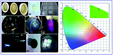
Single crystalline nano thin phosphor films of (Na0.5R0.5)MoO4:Ln3+ (R3+ = La, Gd), (Ln3+ = Eu, Tb, Dy, Yb/Er) have been deposited on quartz substrates by pulsed laser deposition (PLD) technique. In this work, we clearly explained the target preparation, pre-deposition cleaning of substrates using piranha cleaning, and optimized growth conditions of the thin films. The deposition was carried out using an Nd-YAG laser (λ = 1064 nm) in an ultra-high vacuum (UHV) with an oxygen back pressure of 300 mTorr at different substrate temperatures. To examine the crystal structure, 3D surface topography and film thickness, the as-deposited samples were characterized by X-ray diffraction (XRD), atomic force microscopy (AFM) and scanning electron microscopy (SEM), respectively. The thin phosphor films possess a scheelite tetragonal crystal structure with the space group I41/a. The down-conversion luminescence properties of Eu3+, Tb3+, Dy3+ doped (Na0.5R0.5)MoO4 phosphor films were studied in detail. Under 980 nm NIR laser excitation, the Yb3+/Er3+ doped (Na0.5R0.5)MoO4 thin films show intense up-converted green emission identified at 524 nm due to the transition from the populated 2H11/2 level to 4I15/2 ground level of the erbium ion. The fluorescence decay time for the major transitions in (Na0.5R0.5)MoO4 when doped with Eu3+ (5D07F2), Tb3+ (5D47F5), Dy3+ (4F9/26H13/2) and Yb3+/Er3+ (2H11/24I15/2) are determined and to assess the color richness, the CIE color coordinates were also calculated. The obtained results suggested that the potential (Na0.5R0.5)MoO4:Ln3+ thin phosphor films can serve as an excellent material for electro/cathodo-luminescence and display applications.


1. Introduction

The growth of high quality single crystalline ceramic thin films with improved physical and chemical properties has received increasing interest due to their abundant scientific and technological applications in electronic and optoelectronic devices.1–3 Numerous well-known thin film techniques including chemical bath deposition, sputtering, polymerization method, electro deposition, metal–organic chemical vapor deposition, molecular beam epitaxy and pulsed laser deposition (PLD), are widely used to prepare a variety of thin film materials such as molybdates,4 tungstates,5 vanadates,6 and fluorides,7 etc. Among them, PLD is a versatile technique to fabricate multicomponent thin film materials in which raster scanning of high energy pulsed laser ablates the target material and produces the plasma plume.8,9

The high temperature reaction between ablated ions/molecules in the plume with the background gas results in scattering, expansion of angular spreading of the plume and then the number of eroded species trying to move towards the substrates.10 The mean free path of the ablated plume particles in the background gas is strongly depends on the pressure and type of the gas used.10 Then, highly forward directed plasma plume reach the substrates with specific kinetic energy which deposits it as a thin film on the substrates and distributed over wider areas.10 For the growth of complex thin film materials, the stoichiometry of the target material is preserved in the thin film which is the main advantage of the PLD technique. The PLD is a rapid, most simple technique and it has several important features which includes excited oxidizing species, instant deposition, high deposition rate, environmentally clean, small target size, deposition in inert or high pressure gas, and provides better crystalline films, etc.10 McKittrick et al. synthesized Y2O3:Eu3+ thin phosphor films deposited using metallorganic chemical vapor deposition (MOCVD) at 600 °C for 8 h.11 The results suggesting that the emission intensity of Y2O3:Eu3+ film is increases with increasing the post-deposition annealing treatment at 850 °C for 24 h. Li et al. fabricated (Sr,Ba)2SiO4:Eu2+ thin phosphor film using magnetron sputtering and found that the emission intensity reaches maximum at a post-deposition annealing to 1000 °C.12 To avoid the aforesaid drawbacks, PLD is an alternative technique used for multi-component coating and extremely cutthroat in controlling the thickness of the film, despite the intricacy of crystal chemistry in comparison to the other film growth methods.10

To obtain good quality thin films with enhanced physical and chemical properties, it is necessary to investigate the key factors that were influences the film thickness, growth rate and surface morphology and its properties. In general, thin film growth per laser pulse depends strongly on the distance between the target and substrate, pressure of background gas, type of substrate, deposition temperature, size of the laser spot, wavelength and energy density of the laser pulse.10 Nowadays, laser rastering system attached into PLD technique has been used to fabricate a homogeneous and large scale thin film.13 In the application point of view, aforesaid reasons make the PLD technique become unique and most suitable for the growth and fabrication of good quality micro/nano thin films for complex ceramic materials.

Rare earth activated metal molybdates and tungstates with scheelite crystalline phase have gained colossal interest and considered as an important class of phosphor material owing to their brilliant optical properties, high thermal conductivity, adequate stability in higher temperature and vacuum. These properties explain their significance to the applications in the area of flat-panel displays,4,14 electroluminescence displays,15 field emission displays,16 solar cell,17 white LEDs,18 etc. The compound (Na0.5La0.5)MoO4 (NLM) and (Na0.5Gd0.5)MoO4 (NGM) possess a scheelite crystalline phase in which trivalent lanthanum, gadolinium ions and monovalent sodium ions are arbitrarily distributed in dodecahedral positions of the tetrahedral symmetry.19,20 The molybdenum metal ion is situated at the centre of the tetrahedral site and each Mo6+ ion is surrounded by four equivalent oxygen atoms at the corners of the tetrahedra (Td). In the MoO42− tetrahedra, interatomic distances between the Mo and O atoms is equal to the sum of their ionic radii and do not depend on the composition of dodecahedral site.21 Further, the important characteristic of scheelite crystals is high possibility of electrodipole inter-Stark transitions of rare-earth ions in these crystals leads to higher luminescence intensity and high optical absorption bands.21 In order to achieve a novel red, green, yellow emitting thin phosphor films with proper Commission Internationale de L'Eclairage (CIE) chromaticity coordinates, Eu3+, Tb3+, and Dy3+ ions are the best choice to be an activator ions in any host for DC luminescence applications. Similarly, Yb3+ (sensitizer) Er3+ (activator) are used as a good luminescence centres for upconversion process.20 The advantage of (Na0.5R0.5)MoO4 crystal structure doped with lanthanide ions Ln3+ (Ln = Eu, Tb, Dy, Yb/Er) used as laser materials,21 in which Na+, R3+/Ln3+ are randomly distributed in the dodecahedral sites occupy the same crystallographic locations results in broadening of absorption bands and luminescence of Ln3+ is caused by crystal field non-uniformity.21

To the best of our knowledge, the growth of (Na0.5R0.5)MoO4 (R = La, Gd) doped with Ln3+ (Ln = Eu, Tb, Dy, Yb/Er) thin phosphor films by laser ablation of ceramic target in an oxygen atmosphere and their luminescence properties have not yet been reported. For the first time, we report on the growth of nano thin phosphor films of (Na0.5R0.5)MoO4:Ln3+ fabricated on the quartz substrate by PLD technique. Herein, we clearly demonstrated the preparation of target, pre-deposition cleaning of substrates and procedure to synthesize the thin phosphor films. The as-synthesized nano thin phosphor films were characterized by X-ray diffraction pattern (XRD), atomic force microscopy (AFM), scanning electron microscope (SEM), and energy dispersive X-ray analysis (EDX). Further, the up-conversion and down-conversion luminescence properties of Ln3+ doped (Na0.5R0.5)MoO4 thin phosphor films were investigated. The Commission Internationale del'Eclairage (CIE) color chromaticity co-ordinates, fluorescence decay time and the photometric parameters have also been calculated and discussed.

2. Experimental details

The Na0.5R0.5(MoO4):Ln3+ (R = La, Gd and Ln = Eu, Tb, Dy, Yb/Er) nano thin phosphor films were successfully deposited onto the quartz substrates by using the PLD technique at a substrate temperature of 600 °C with an ambient oxygen partial pressure of 300 m Torr. Fig. 1(a–i) shows the photographs of various experimental steps involved for the growth of thin films and are described as follows.
image file: c4ra11274a-f1.tif
Fig. 1 Photograph of various experimental procedures demonstrated (a) pelletized ceramic target, (b) annealed target, (c), substrate cleaning, (d) loading of target, (e) substrates loading, (f) removal of impurities in UHV chamber (glow discharge), (g) laser ablation, (h) ablated target, (i) as-deposited thin films.

2.1 Target preparation

In order to prepare robust and highly dense ceramic target for laser ablation, stoichiometric amounts of starting materials such as Na2CO3, La2O3, MoO3, and Ln2O3 (Ln = Eu, Tb, Dy, Yb, Er) were grounded in an agate mortar pestle for 2 h. The doping concentrations of Ln3+ were optimized in our previous work22 and kept at constant (0.08 M) for all the Ln3+ ions. Then the powder mixture was pressed and pelletized into a disk at a pressure of 6 tons without using any binders. To remove the volatile impurities, avoid pores and cracks, promote densification, and to facilitate atomic diffusion throughout the target,10 the as-prepared pellet was annealed at 900 °C for 3 h. The strong and dense pellets with 2.2 cm diameter and 0.4 cm thickness are obtained and used as a target for laser ablation.

2.2 Pre-deposition cleaning of substrates

The thin films were grown on 1 cm × 1 cm quartz substrates (with 0.7 mm thickness) that were cut from the same quartz wafer. Prior to the deposition, each piece of substrates was chemically cleaned using the piranha cleaning procedure.23,24 The pre-deposition cleaning of substrates is as follows.

(i) First, all the substrates were immersed into a piranha solution (H2SO4[thin space (1/6-em)]:[thin space (1/6-em)]H2O2 = 3[thin space (1/6-em)]:[thin space (1/6-em)]1 ratio) at 80–90 °C for 30 minutes. After cooled to the room temperature, the substrates were then rinsed in double distilled (DD) water.

(ii) Followed by dipping in HF[thin space (1/6-em)]:[thin space (1/6-em)]H2O (1[thin space (1/6-em)]:[thin space (1/6-em)]50 ratio) mixture solution for 30 s at room temperature and rinsed with DD water.

(iii) Finally, dipping in H2O[thin space (1/6-em)]:[thin space (1/6-em)]HCl[thin space (1/6-em)]:[thin space (1/6-em)]H2O2 (6[thin space (1/6-em)]:[thin space (1/6-em)]1[thin space (1/6-em)]:[thin space (1/6-em)]1) mixture solution at 80–90 °C for 30 minutes and rinsed with DD water and then dried.

2.3 Growth of Na0.5R0.5(MoO4):Ln3+ (Ln = Eu, Tb, Dy, Yb/Er) nano thin phosphor films

The Na0.5La0.5(MoO4):Ln3+ nano thin films were fabricated on to the quartz substrates and the deposition was carried out in an ultra-high vacuum (UHV) unit along with Nd-YAG laser fundamental (λ = 1064 nm) was used during the ablation process. After cleaning the substrates by aforesaid piranha cleaning procedure, the substrates and targets were mounted on the respective holders using a silver paste (to ensure good contact) into the UHV chamber. In order to clean the vacuum chamber prior to the deposition, high plasma current (DC current) has been applied to remove the unwanted impurities by glow discharge. Subsequently, to create UHV, the chamber was primarily evacuated to a pressure of 5 × 10⁻⁶ mbar. Next, the chamber was backfilled with ambient oxygen (99.99%) partial pressure of 300 mTorr. Further, to achieve high quality thin films, the substrates (attached with substrate holder) were thermally annealed and maintained at a temperature of 300 to 600 °C. In order to ensure the uniformity of ablation and plasma plume, the target material was connected to a rotating head so as to enable homogeneous laser ablation on the surface of the target. The distance between the quartz substrate and ceramic target were kept at 45 mm space. The target was ablated using the laser output approximately 200 mJ per pulse operated at a repetition rate of 10 Hz with the pulse duration of 6 ns. The ablated species interact with background gas and directed forwardly towards the quartz substrates. After the deposition of thin phosphor films, the UHV chamber was allowed to cool down to room temperature. Similar kind of experimental procedure was repeated for Na0.5Gd0.5(MoO4) sample doped with Eu3+, Tb3+, Dy3+ and Yb3+/Er3+ respectively by keeping all the parameters constant.

2.4 Characterization

The Philips X'Pert PRO unit from PANalytical's diffractometer were used to record the XRD patterns and performed with Cu Kα radiation (λ = 0.15406 nm), scanning rate of 0.05° s−1. The elemental analysis and the surface morphology of the as-deposited thin films were inspected using scanning electron microscope (SEM JEOL JSM-840). The surface topography of the thin phosphor films was examined using atomic force microscopy (NTEGRA PRIMA-NTMDT, Ireland). Down conversion luminescence properties and fluorescence decay time of the thin phosphor films were investigated using Agilent Cary Eclipse spectrophotometer (G9800AA) operated with a 150 W xenon lamp as the excitation source. Up-conversion luminescence and the corresponding lifetime values (980 nm laser excitation from an optical parametric oscillator) are analyzed using a combination of a 0.25 m monochromator (CS-260; Oriel, Rochester, NY), photomultiplier tube (70680; Oriel, Stratford, CT), lock-in amplifier, and oscilloscope.

3. Results and discussion

3.1 Powder X-ray diffraction analysis and morphological investigations

The phase purity and crystalline nature of the (Na0.5R0.5)MoO4:Ln3+ (R = La, Gd and Ln = Eu3+, Tb3+, Dy3+, Yb3+/Er3+) thin phosphor films were analyzed using X-ray diffraction patterns (XRD) that were shown in Fig. 2(a and b). The XRD patterns elucidates that the as-prepared thin films were crystallizes in the scheelite crystal structure (space group I41/a). The crystal structure of (Na0.5R0.5)MoO4:Ln3+ is isostructural to the CaWO4 scheelite tetragonal structure in which Na+ and R3+/Ln3+ atoms replace the Ca2+ sites and occupy the dodecahedral sites in the tetrahedral symmetry.19,20,22 In the centre of the tetrahedra, Mo6+ atoms are occupying W6+ locations forming isolated [MoO4]2- group when surrounded with four equivalent O2− atoms which are located at the four apex angles.25 The degree of tetrahedral distortion is given by the equation,26
 
image file: c4ra11274a-t1.tif(1)

image file: c4ra11274a-f2.tif
Fig. 2 XRD patterns of pulsed laser deposited (a) (Na0.5La0.5)MoO4, (b) (Na0.5Gd0.5)MoO4 doped with Ln3+ (Ln = Eu, Tb, Dy, Yb/Er) thin phosphor films, respectively.

The Na+ and R3+/Ln3+ atoms are bonded and coordinated with oxygen atoms in the dodecahedral sites (CN = 4 + 4) by two sets of bond distance.26 The molybdenum atom is in a slightly distorted tetrahedral oxygen coordination (MoO4) with identical Mo–O bond distances (CN = 4).26 Such a distorted dodecahedron influences the homogeneity of the crystal field around the optically active ions, inducing a considerable enhancement in the intensity of the absorption and emission spectrum.20,25,27 The degree of dodecahedral distortion is given by

 
image file: c4ra11274a-t2.tif(2)

Kuzmicheva et al. reported that, since the ionic radius of lanthanum (rLa = 1.17 Å) is higher than gadolinium (rGd = 1.05 Å), the lattice parameters were increased for NLM than NGM, which results in the size of the dodecahedral site increases.26,28 Hence, the dodecahedral site in NLM is distorted in higher degree rather than NGM.26,28 The indexed peaks in the XRD patterns are consistent with the Joint Committee on Powder Diffraction Standards (JCPDS) and matches well with 79-2243 and 25-0828 of scheelite tetragonal (Na0.5La0.5)MoO4 and (Na0.5Gd0.5)MoO4, respectively. No other impurity peaks were detected in the XRD pattern, vindicating good quality thin films were successfully synthesized and exhibits single crystalline nature. The doping of Ln3+ (Eu, Tb, Dy, Yb/Er) successfully replaces the R3+ (La, Gd) and does not alter the crystal structure of the host. The Fig. S2 and S3 shows the EDX spectra which confirms the existence of respective elements in Ln3+ doped (Na0.5R0.5)MoO4 thin film samples.

As a representative result, Fig. 3(a and b) shows the low and high magnification SEM image of the (Na0.5La0.5)MoO4:Eu3+ thin phosphor film grown at 600 °C with 300 mTorr. The as-deposited phosphor film consists of homogeneous, highly ordered circular grains with well-defined boundaries with an average grain size vary approximately between 225 nm to 250 nm. The corresponding cross-sectional view of the SEM image suggesting that the average thickness of the thin phosphor films are found to be nearly 275 nm covering the entire surface area of the substrate (Fig. 3c). Using AFM technique the surface topography, roughness and line profile of the as-grown thin phosphor films were investigated. Fig. 4(a and b) shows the 3D AFM images of (Na0.5La0.5)MoO4 doped with Eu3+ and Yb3+/Er3+ thin films, respectively and the scan was performed on 4 × 4 μm2 area. From the AFM images, it is observed that the as-deposited thin films appeared to be of smooth surface and the particles are homogeneously distributed, less agglomerative. However, a few grains in the thin film are appeared to be larger size (∼500 nm) and this is due to increased ablation rate of the target by laser beam which deposits more species on the substrate. At 300 mTorr, the average roughness and root mean square of the as-grown thin films were measured to be 25.85 nm, 28.32 nm and 34.44 nm, 39.75 nm for Eu3+ and Yb3+/Er3+ doped (Na0.5La0.5)MoO4, respectively. Fig. 5a shows the 2D surface topography and the corresponding cross sectional line profile were measured at three different points along the white line indicated on the image (Fig. 5(b–d)).


image file: c4ra11274a-f3.tif
Fig. 3 (a) Low magnification, (b) high magnification, (c) cross-sectional, SEM image of the as-deposited (Na0.5La0.5)MoO4:Eu3+ thin films.

image file: c4ra11274a-f4.tif
Fig. 4 Representative 3D surface topography of the pulsed laser deposited (Na0.5La0.5)MoO4 doped with (a) Eu3+, (b) Yb3+/Er3+ thin films, respectively.

image file: c4ra11274a-f5.tif
Fig. 5 (a) 2D surface scan image of the (Na0.5La0.5)MoO4:Eu3+ thin film. The corresponding vertical cross sectional line profile taken at (a) 1160 nm, (b) 1960 nm, (c) 2750 nm, in 4 × 4 μm2 scan area, respectively.

3.2 Down conversion luminescence properties of laser ablated (Na0.5R0.5)MoO4:Ln3+ (R = La3+, Gd3+ and Ln = Eu3+, Tb3+, Dy3+) thin phosphor films

The photoluminescence excitation spectra of Ln3+ doped NLM and NGM phosphors have been well investigated and reported in our earlier work.19,20,22 Practically, the thin film with lower crystallinity gives weak luminescence intensity. In order to improve the crystalline nature of the samples, the phosphor films were synthesized at different substrate temperature (300 to 600 °C) with fixed oxygen pressure (300 mTorr). From Fig. 6, it is observed that the substrate temperature increases from 300 °C to 600 °C, the luminescence intensity of (Na0.5La0.5)MoO4:Eu3+ thin film is also increased due to improved crystalline nature of the thin films. The XRD patterns of (Na0.5La0.5)MoO4:Eu3+ thin films shown in Fig. S1 supports improved crystalline nature of films when the deposition temperature is increases to 600 °C which play a crucial role in increasing the luminescence properties. Fig. 7a shows the photoluminescence emission spectra of (Na0.5La0.5)MoO4:Eu3+ thin film excited at 394 nm UV irradiation. It is well-known that, Eu3+ has the 4f6 electronic configuration with 7F0 ground state in which the major emission lines are originated from populated 5D0 level to 7FJ ground levels (J = 0, 1, 2, 3, 4) and the major lines are 5D07F1 (due to magnetic dipole transition), 5D07F2 (due to electric dipole transition).20,22,29 Upon excitation, the PL emission spectra of (Na0.5La0.5)MoO4:Eu3+ consists of four peaks noticed at 588 nm, 614 nm, 651 nm and 698 nm are attributed to the transitions of 5D07F1, 5D07F2, 5D07F3, 5D07F4, Eu3+ ion, respectively. Among all the emission peaks, the electric dipole transition 5D07F2 is hypersensitive and much stronger than the other peaks which are necessary to improve the color purity of the red phosphor. According to the selection rule, narrow peak observed at 614 nm corresponding to the transition 5D07F2 is due to the shielding effect of 4f electrons by 5s and 5p electrons in the outermost shells of Eu3+.30,31 The transition 5D07F1 (orange light) or the transition 5D07F2 (red light) strongly relies on the local symmetry of Eu3+ ions; i.e., when the Eu3+ ions occupy the inversion center sites, the transition 5D07F1 should be predominant, and when the Eu3+ ions occupy the lower symmetry sites, the transition 5D07F2 should be predominant.22,32 In the case of (Na0.5La0.5)MoO4:Eu3+ scheelite tetragonal structure, the dominance of 5D07F2 transition vindicates that Eu3+ ions were located at sites without inversion symmetry (C3ν symmetry). The ratio of integrated emission intensities of the two transitions 5D07F1 and 5D07F2 is called as the asymmetry ratio which determines the degree of distortion from the inversion symmetry of Eu3+ ions.33 The R/O ratio values calculated for NLM, NGM are found to be 4.89, 4.81, respectively, showing that the hypersensitive electric dipole transition dominates with magnetic dipole transition.
image file: c4ra11274a-f6.tif
Fig. 6 Emission intensity of (Na0.5La0.5)MoO4:Eu3+ as a function of different substrate temperature.

image file: c4ra11274a-f7.tif
Fig. 7 Down-conversion luminescence spectra of (Na0.5La0.5)MoO4 doped with (a) Eu3+, (b) Tb3+, (c) Dy3+ thin phosphor films, respectively deposited at 600 °C with 300 mTorr pressure.

The Tb3+ ion has the electronic configuration 4f8 with 7F6 ground state. Under 294 nm ultraviolet excitation, Tb3+ doped samples show the characteristic transitions from populated 5D4 level to 7FJ ground levels (J = 6, 5, 4, 3). Fig. 7b shows the PL emission spectra of Tb3+ doped (Na0.5La0.5)MoO4 thin phosphor films, exhibits four emission bands observed at 489 nm, 543 nm, 587 nm, and 621 nm and are assigned for the transitions 5D47F6, 5D47F5, 5D47F4, 5D47F3 of Tb3+ ions, respectively.19,20,34 Generally, the luminescence intensity of the transition 5D47F5 is much higher than the other transitions. The intensity and peak position of 5D47F5 transition, strongly influenced by the symmetry at the metal ion site and nature of bonding with coordinating ligand.34 The green emission peak is instigated due to characteristic 4f electrons of Tb3+ ions centered at 543 nm which corresponds to magnetic dipole allowed transition 5D47F5 which is unaffected by the site symmetry of Tb3+ ion. The hypersensitive and most intense 5D47F5 transition satisfies the selection rule ΔJ = ±1 and much stronger than other transition with ΔJ = 3, 4, 6 (electric dipole transitions).35

The Dy3+ ion has also chosen to be an activator which has the electronic configuration of 4f9 with 6H15/2 ground state. In general, the blue emission is originated from the transition 4F9/26H15/2. Whereas the yellow emission is originated from the hypersensitive transition 4F9/26H13/2 belongs to a forced electric dipole transition allowed only Dy3+ ions occupy non-inversion symmetry.36 The transition 4F9/26H13/2 can be influenced by the surrounding chemical environment of Dy3+ ions19,20 but, the intensity ratio between the blue band and yellow band varies with respect to the hosts. Becerro et al. reported that for Dy3+ doped GdPO4 the transition 4F9/26H15/2 was predominant when compared with 4F9/26H13/2.37 But in the case of molybdates, it is reported that the intensity of yellow band originated due to 4F9/26H13/2 transition is high when compared with the blue band due to the transition 4F9/26H15/2.19,20 Fig. 7c shows the emission spectra of Dy3+ doped (Na0.5La0.5)MoO4 thin phosphor films excited at 390 nm and the corresponding emission is originated due to the transition from the populated 4F9/2 levels to the 6HJ (J = 15/2, 13/2) ground levels of Dy3+ ions, respectively.19,20 The integral intensity of the blue band observed at 482 nm is higher than that of the yellow band (hypersensitive to the chemical environment) noticed at 569 nm which figure out the information on the site occupancy of Dy3+ in the scheelite tetragonal (Na0.5R0.5)MoO4 crystal structure. Further, Fig. 8(a–c) shows the photoluminescence properties of Ln3+ doped (Na0.5Gd0.5)MoO4 thin film samples were investigated. The down conversion luminescence properties of Ln3+ doped (Na0.5Gd0.5)MoO4 are similar to that those of (Na0.5La0.5)MoO4:Ln3+ and does not show any remarkable variation with respect to peak position. However, the luminescent intensities Ln3+ doped NLM are slightly higher than that of NGM. Kuzmicheva et al. explained that, due to difference in ionic radius (rLa > rGd) the degree of dodecahedral distortion in NLM higher than NGM and.26,28 Such a distorted dodecahedron influences the homogeneity of the crystal field around the optically active ions, inducing a slight improvement in the emission intensity of NLM than NGM.26,28


image file: c4ra11274a-f8.tif
Fig. 8 Down-conversion PL graph of (a) Eu3+ (b) Tb3+, (c) Dy3+ doped (Na0.5Gd0.5)MoO4 thin films deposited at 600 °C with 300 mTorr pressure.

3.3 Up-conversion luminescence properties of pulsed laser deposited (Na0.5R0.5)MoO4:Yb3+/Er3+ (R = La3+, Gd3+) thin phosphor films

Fig. 9a illustrates the up-conversion luminescence spectra of pulsed laser deposited (Na0.5R0.5)MoO4:Yb/Er thin phosphor films. The presence of intense up-converted emission lines in the green region accompanied with weak emission in the red region which are mainly originated due to the transitions of Er3+ ion. Under 980 nm laser excitation, the emission spectra consists of three characteristic up-converted lines observed in the visible region at 524 nm, 550 nm, 653 nm which are assigned for the transitions 2H11/24I15/2, 4S3/24I15/2, and 4F9/24I15/2, respectively implies a strong ground state absorption of Er3+ ion. The emission spectra are ruled by an intense up-converted green emission noticed at 524 nm due to the transition from the populated 2H11/2 levels to 4I15/2 ground levels of Er3+ ion. The hypersensitive transition 2H11/24I15/2 is much stronger than the other transitions.
image file: c4ra11274a-f9.tif
Fig. 9 (a) Up-conversion luminescence spectra of Yb3+/Er3+ doped (Na0.5R0.5)MoO4, (b and c) luminescence decay profile of 2H11/24I15/2 transition in Yb3+/Er3+ doped NLM and NGM, respectively, (d) their corresponding CIE diagram.

Under 980 nm infrared laser excitation on Yb/Er doped (Na0.5R0.5)MoO4 thin films, Yb3+ ions are initially excited from 2F7/2 level to the 2F5/2 level via well known ground state absorption process.20 Also, the laser excitation populates the electrons from the 4I15/2 ground level to the 4I11/2 level of Er3+ ions. Then, the excited 2F5/2 level of ytterbium ions promotes more energy to the populated 4I11/2 level of Er3+ through the energy transfer process.20 Consequently, the 4F7/2 level of Er3+ is excited from 4I11/2 of Er3+ through the excited state absorption process and then relaxed non-radiatively into the 2H11/2 level. Next, 2H11/2 and 4S3/2 levels in Er3+ ion are partly decays non-radiatively into 4S3/2 and 4F9/2 levels, respectively. At last, 2H11/2, 4S3/2 and 4F9/2 levels radiatively depopulated in the 4I15/2 ground level by emitting intense up-converted visible light photons with a wavelength of 524 nm, 550 nm, and 653 nm, respectively. The integrated up-conversion emission intensity ratio of the transitions 2H11/24I15/2 (green) to 4S3/24I15/2 (red) for (Na0.5La0.5)MoO4:Yb/Er is found to be 3.453 whereas (Na0.5Gd0.5)MoO4:Yb/Er is determined to be 3.421. Wang and coworkers described that the distribution of Er3+ ions on the surface is of a larger fraction than that of inside the nanometre scale particles.38 Therefore, the interaction among the Er3+ ion and its neighboring crystal lattice becomes poor caused by isotropic coordination of Er3+ ions with higher symmetry results in the transition 2H11/24I15/2 much stronger than the other transitions.20 The concentration quenching effect, dependence of pump power density, energy transfer process, and near-infra red emission properties of Yb/Er doped (Na0.5R0.5)MoO4 (R = Gd) were elaborately discussed in our earlier investigations.20 The upconversion luminescence mechanism explains that the energy is successfully transferred from the Yb3+ (sensitizer) to the Er3+ (activator). In the case of Yb/Er doped NLM and NGM, shape and position of the peaks are almost similar and does not show any remarkable variation in the up-conversion luminescence spectra. Hence, the Yb/Er ions doped samples shows their strong up-conversion luminescence irrespective of the NLM, NGM crystal structures.

3.4 Decay-time and color coordinates measurements

The luminescence decay curves of Ln3+ doped (Na0.5R0.5)MoO4 were fitted well with the single exponential function and is given by
 
image file: c4ra11274a-t3.tif(3)
where I0 is the luminous intensity at time t = 0, t is the time after excitation, and the decay life time is indicated as τ. Fig. S4(a–c) shows the PL decay profile of major emission lines in Eu3+, Tb3+, and Dy3+, doped with (Na0.5R0.5)MoO4 thin phosphor films and the corresponding values are summarized in Table S1. Fig. 9b and c shows the decay time profile for the transition 2H11/24I15/2 in Yb3+/Er3+ doped (Na0.5R0.5)MoO4 thin films and the values are determined to be 8.5 μs (for R = La) and 8.1 μs (for R = Gd). The color chromaticity coordinates are estimated using the Commission of Internationale del'Eclairage (CIE) 1931 color matching functions.20 Fig. S5 and S6 shows the CIE plot of Eu3+, Tb3+ and Dy3+ doped (Na0.5R0.5)MoO4 thin films. Under 980 nm NIR excitation, the color chromaticity coordinates of Yb3+/Er3+ doped (Na0.5La0.5)MoO4, and (Na0.5Gd0.5)MoO4 were calculated and found to be x = 0.184, y = 0.779 and x = 0.183, y = 0.776, respectively and the corresponding CIE diagram is shown in Fig. 9d. Further, the photometric properties of the as-synthesized thin films such as color rendering index, color correlated temperature, and luminous efficacy of radiation were calculated and provided in Table S1. The presence of strong up/down-conversion luminescent intensity indicates the good crystalline nature of nano sized phosphor films. The novel (Na0.5R0.5)MoO4:Ln3+ nano thin phosphor films could serve as an excellent material for electroluminescence devices, flat-panel display applications and other opto-electronic applications.

4. Conclusions

In summary, we synthesized the nano-sized single crystalline (Na0.5R0.5)MoO4:Ln3+ (R3+ = La, Gd), (Ln3+ = Eu, Tb, Dy, Yb/Er) ceramic thin phosphor films deposited on quartz substrates by pulsed laser deposition technique using Nd-YAG laser source in an ultra-high vacuum. The clear demonstrations of the various experimental steps involving the growth of thin film have been discussed. The XRD analysis reveals that the as-deposited (Na0.5R0.5)MoO4:Ln3+ films posses scheelite tetragonal crystal structure in which molybdenum ions are located in the centers of the tetrahedra and R3+/Ln3+ atoms occupy the dodecahedral positions in the tetrahedral symmetry. The presents of all the elements in Ln3+ doped (Na0.5R0.5)MoO4 thin phosphor films were confirmed by EDX analysis. The 3D surface topography, grain size distribution, roughness and rms value are investigated by AFM technique. The SEM image clearly depicts that the average thickness of the thin films was determined to be 275 nm. The down-conversion photoluminescence properties of the thin phosphor film were investigated in detail. Under optical excitation, Eu3+, Tb3+ and Dy3+ doped samples show their characteristic luminescence in red, green, yellow region due to the transitions 5D07F2, 5D47F5, 4F9/26H13/2, respectively. Upon 980 nm NIR laser pumping, Yb3+/Er3+ doped (Na0.5R0.5)MoO4 thin films exhibits strong green due to the hypersensitive transition 2H11/24I15/2 noticed at 524 nm. The CIE color chromaticity coordinates, fluorescence decay time and other photometric parameters of Ln3+ doped (Na0.5R0.5)MoO4 thin films were estimated. The current results suggest that the deposition of high quality single crystalline phosphor thin films could serve as a superb material for electro/cathodo-luminescence devices, display applications and other solid-state lighting appliances.

Acknowledgements

The authors acknowledge Alagappa University-Karaikudi, and SAIF-IIT Bombay for extending their instrumentation facilities for characterization.

References

  1. H. Yang, W. Wang, Z. Liu, W. Yanga and G. Li, CrystEngComm, 2014, 16, 3148 RSC.
  2. Y. Zhang and J. Hao, J. Mater. Chem. C, 2013, 1, 5607 RSC.
  3. K. Mahmood, B. S. Swain and H. S. Jung, Nanoscale, 2014, 6, 9127 RSC.
  4. S. W. Park, B. K. Moon, B. C. Choi, J. H. Jeong, J. S. Bae and K. H. Kim, Curr. Appl. Phys., 2012, 12, S150 CrossRef.
  5. P. A. Atanasov, R. I. Tomov, J. Perriere, R. W. Eason, N. Vainos, A. Klini, A. Zherikhin and E. Millon, Appl. Phys. Lett., 2000, 76, 2490 CrossRef CAS.
  6. D. Barreca, L. E. Depero, V. D. Noto, G. A. Rizzi, L. Sangaletti and E. Tondello, Chem. Mater., 1999, 11, 255 CrossRef CAS.
  7. M. Yanagihara, M. Z. Yusop, M. T. anemura, S. Ono, T. Nagami, K. Fukuda, T. Suyama, Y. Yokota, T. Yanagida and A. Yoshikawa, APL Mater., 2014, 2, 046110 CrossRef.
  8. P. A. Shaikh, V. P. Thakare, D. J. Late and S. Ogale, Nanoscale, 2014, 6, 3550 RSC.
  9. P. K. Patel, K. L. Yadav and G. Kaur, RSC Adv., 2014, 4, 28056 RSC.
  10. R. Eason, in Pulsed laser deposition of thin films:applications-led growth of functional materials, ed. R. Eason, Wiley-Interscience a John Wiley & Sons, Inc., Hoboken, New Jersey, 2007, pp. 1–682 Search PubMed.
  11. J. McKittrick, C. F. Bacalski and G. A. Hirata, J. Am. Ceram. Soc., 2000, 83, 1241 CrossRef CAS.
  12. L. Li, J. Zheng, Y. Zuo, B. Cheng and Q. Wang, J. Lumin., 2014, 152, 234 CrossRef CAS.
  13. H. Yang, W. Wang, Z. Liu and G. Li, CrystEngComm, 2013, 15, 7171 RSC.
  14. C. Hazra, T. Samanta, A. V. Asaithambi and V. Mahalingam, Dalton Trans., 2014, 6623 RSC.
  15. J. Thirumalai, R. Chandramohan and V. Saaminathan, in Synthesis and Luminescence Properties of EuMoO4 Octahedron-Like Microcrystals, Materials Science and Technology, ed. S. Hutagalung, InTech, 2012, pp. 275–286, ISBN: 978-953-51-0193-2.
  16. L. Hou, S. Cui, Z. Fu, Z. Wu, X. Fu and J. H. Jeong, Dalton Trans., 2014, 5382 RSC.
  17. C. Xueqin, L. Li, W. Xiantao, C. Yonghu, Z. Weiping and Y. Min, J. Nanosci. Nanotechnol., 2011, 11, 9543 CrossRef.
  18. A. M. Kaczmarek and R. V. Deun, Chem. Soc. Rev., 2013, 42, 8835 RSC.
  19. R. Krishnan, J. Thirumalai, S. Thomas and M. Gowri, J. Alloys Compd., 2014, 604, 20 CrossRef CAS.
  20. R. Krishnan and J. Thirumalai, New J. Chem., 2014, 38, 3480 RSC.
  21. G. M. Kuzmicheva, A. V. Eremin, V. B. Rybakov, K. A. Subbotin and E. V. Zharikov, Russ. J. Inorg. Chem., 2009, 54, 854 CrossRef.
  22. R. Krishnan, J. Thirumalai, I. B. S. Banu and R. Chandramohan, J. Mater. Sci.: Mater. Electron., 2013, 24, 4774 CrossRef CAS.
  23. H. J. Nam, J. Cha, S. H. Lee, W. J. Yoo and D.-Y. Jung, Chem. Commun., 2014, 50, 1458 RSC.
  24. A. Datar, R. Oitker and L. Zang, Chem. Commun., 2006, 1649–1651 RSC.
  25. D. Zhao, W.-D. Cheng, H. Zhang, S.-P. Huang, M. Fang, W.-L. Zhang and S.-L. Yang, J. Mol. Struct., 2009, 919, 178 CrossRef CAS.
  26. G. M. Kuz'micheva, V. B. Rybakov, E. V. Zharikov, D. A. Lis and K. A. Subbotin, Inorg. Mater., 2006, 42, 303 CrossRef.
  27. D. Zhao, F. Li, W. Cheng and H. Zhang, Acta Crystallogr., Sect. E: Struct. Rep. Online, 2010, E66, i36 Search PubMed.
  28. G. M. Kuzmicheva, A. V. Eremin, V. B. Rybakov, K. A. Subbotin and E. V. Zharikov, Russ. J. Inorg. Chem., 2009, 54, 854 CrossRef.
  29. A. K. Parchur and R. S. Ningthoujam, RSC Adv., 2012, 2, 10859 RSC.
  30. I. Omkaram, B. Vengala Rao and S. Buddhudu, J. Alloys Compd., 2009, 64, 565 CrossRef.
  31. X. Xiao, G. Lu, S. Shen, D. Mao, Y. Guo and Y. Wang, Mater. Sci. Eng., B, 2011, 176, 72 CrossRef CAS.
  32. A. K. Parchur, R. S. Ningthoujam, S. B. Rai, G. S. Okram, R. A. Singh, M. Tyagi, S. C. Gadkari, R. Tewari and R. K. Vatsa, Dalton Trans., 2011, 7595 RSC.
  33. A. Katelnikovas, J. Plewa, S. Sakirzanovas, D. Dutczak, D. Enseling, F. Baur, H. Winkler, A. Kareiva and T. Justel, J. Mater. Chem., 2012, 22, 22126 RSC.
  34. W. M. Pontusch ka, L. S. Kanashiro and L. C. Courrol, Glass Phys. Chem., 2001, 27, 37 CrossRef CAS.
  35. G. Blasse and B. C. Grabmaier, in Luminescent materials, Springer-Verlag Telos, New York, 1994, pp. 1–232 Search PubMed.
  36. S. Dutta, S. Som and S. K. Sharma, Dalton Trans., 2013, 9654 RSC.
  37. A. I. Becerro, S. Rodriguez-Liviano, A. J. Fernandez-Carrion and M. Ocaña, Cryst. Growth Des., 2013, 13, 526 CAS.
  38. X. Wang, X. Kong, G. Shan, Y. Yu, Y. Sun, L. Feng, K. Chao, S. Lu and Y. Li, J. Phys. Chem. B, 2004, 108, 18408 CrossRef CAS.

Footnote

Electronic supplementary information (ESI) available: Fig. S1–S6 and Table S1. See DOI: 10.1039/c4ra11274a

This journal is © The Royal Society of Chemistry 2014