The effect of a thin gold layer on graphene: a Raman spectroscopy study

Martin Kalbac*a, Vaclav Valesa and Jana Vejpravovab
aJ. Heyrovský Institute of Physical Chemistry of the ASCR, v.v.i., Dolejškova 3, 182 23 Prague 8, Czech Republic. E-mail: kalbac@jh-inst.cas.cz
bInstitute of Physics of the ASCR, v.v.i., Na Slovance 2, 182 21 Prague 8, Czech Republic

Received 26th September 2014 , Accepted 6th November 2014

First published on 10th November 2014


Abstract

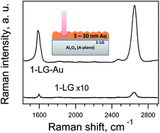
An understanding of interactions between graphene and its surroundings is crucial for application of graphene in electronic devices. Raman spectroscopy is a convenient and efficient tool to provide information about the doping, stress and defects in graphene; however application of this method is limited to the Si/SiO2 substrate which provides interference enhancement. Here we present a comprehensive Raman study of the single-layer graphene – sapphire – gold system. Due to plasmons generated in the gold-layer the Raman signal of graphene is significantly enhanced. We study the influence of the gold layer thickness and gold particle size on the enhancement. The analysis of the Raman maps showed that graphene on sapphire is only slightly doped and the spatial distribution of doping is quite homogenous. Also no significant strain was generated in graphene sandwiched by sapphire and gold.


Introduction

Graphene and graphene–metal heterostructures are promising building elements of new electronic and plasmonic devices. Interaction of these new materials and/or their components with the surroundings may significantly modify their electronic structure. This may be beneficial since the properties can be tuned by the environment, but on the other hand it can be limiting at the same time for other applications. In any case it is important to control and understand the interactions between graphene and graphene heterostructures with their surroundings.

The graphene can be prepared by several methods. The most promising procedure is the copper catalysed CVD growth. Recent advances in the latter method allowed production of the high quality graphene films without formation of add-layers.1

Most of the studies of graphene are traditionally performed using SiO2/Si substrate. This substrate is also quite popular since it enables fast optical identification of single-layer graphene. However, the SiO2 introduces several problems, like randomly trapped surface charges, haphazard strain generation, strong affinity to water etc. The single layer graphene (1-LG) as a 2D material has intimate contact with the silicon dioxide substrate through 50% of its total surface area; hence the mutual interactions plays dominant role in the 1-LG response to the applied electric field. Indeed, the charge impurities in SiO2/Si substrate are critical since they lead to electron–hole charge density fluctuations and limit the performance of electronic devices.2 Therefore substitution of the most popular silicon dioxide substrate with other materials, lacking the above mentioned drawbacks, is of high demand. Recently, the so-called high-K materials, possessing at least one-order higher dielectric constant, K like Al2O3 were reported as promising substrates for fabrication of graphene-based transistors.3,4 Because of the large K values they screen very effectively long-range electron–electron interactions and potential fluctuations, thus making Dirac electrons in graphene virtually non-interacting.5

Raman spectroscopy is widely used for the characterization of graphene.6 The popularity of the Raman spectroscopy in studies of graphene arises mainly from the hope that a large amount of information (stress, doping, number of defects, number of layers etc.) can be potentially extracted from these measurements. The important Raman modes are the D (at about 1350 cm−1), G (at about 1585 cm−1), D′ (at about 1610 cm−1) and G′ (at about 2700 cm−1).7 Note that the G mode frequency is strongly dependent on the graphene doping.8 The G′ mode frequency is sensitive to the stress applied on graphene.9 The presence of D and D′ mode in the Raman spectra indicates defects in graphene.10

However, in order to be able to study graphene–substrate interactions efficiently one should be able to obtain sufficiently intense spectra to enable measurements of Raman maps. Unfortunately, these conditions are not fulfilled in most cases, except for the most popular substrate used for the Raman studies: SiO2/Si. Due to an interference effect, the intensity is enhanced by factor of 10–30 depending on the laser excitation energy and oxide layer thickness.11 This is one of the reasons for the high popularity of the SiO2/Si substrate. Even though the signal on the SiO2/Si substrate is enhanced, the intensity is relatively low and performing measurements of Raman maps, which are necessary for the correct characterization of the graphene samples, is a time consuming task. The intensity of the graphene Raman modes is even weaker on other dielectric substrates, since the interference enhancement is missing. The use of high power laser to excite Raman spectra is not possible due to limited stability of graphene. Furthermore the high power lasers induce heating of graphene samples which leads to changes in the Raman spectra ref. 12 and 13. Hence the laser power must be typically limited to about 1 mW.

Consequently, it is challenging to obtain even a single Raman spectrum with sufficient signal/noise ratio. This significantly limits the use of Raman spectroscopy to study such materials despite it would be of high interest.

Some attempts to improve the signal of graphene were published previously.14–18 Using Ag particles the Raman signal enhancement of about 20 times was achieved.19 The gold particles provided sufficient signal enhancement but compromised by the simultaneous increase of the noise level.20 In other studies the benefit of the surface-enhanced Raman scattering was used to study the interaction of the graphene and metal.20,21

The structure of gold deposited on graphene depends on the number of layers and subsequent treatment.22,23 It was found previously that the highest density of gold particles is realized on 1-LG.22 Also the gold can be completely evaporated thus recovering original graphene.22

Although several studies of graphene–metal systems can be found in literature, there are still several open problems regarding the understanding of the graphene–metal interactions. The prerequisite is a proper characterisation and description of the system, which is also lacking in most of the previous studies.

The objective of our work here is a study of graphene on sapphire with various thicknesses of a gold layer. We employed analysis by X-ray diffraction (XRD), X-ray reflectivity (XRR) and atomic force microscopy (AFM) to determine the surface morphology, gold layer thickness and grain size of the gold clusters. Then we performed a study of an enhancement of the Raman signal of graphene. In addition we measured Raman maps on 1-LG and studied distribution of the doping levels and stress in graphene on sapphire substrate.

Results and discussion

The graphene grown on copper substrate was transferred on sapphire using standard PMMA transfer procedure (for details see the Experimental section) and the samples on sapphire substrate were covered with gold layers of various thicknesses. Sapphire substrate represents model dielectrics or a model dielectric system which can be obtained in the form of single crystal with flat surface. Fig. 1 shows the AFM images of 1-LG covered with 5, 10 and 20 nm of gold (for AFM of pristine 1-LG see the ESI file Fig. S2). Already 5 nm thick gold layer forms rather continuous film without visible cracks and it even covers graphene wrinkles perfectly. The 10 nm gold layer makes the surface features only weakly visible and if 20 nm gold layer is deposited, the surface morphology of the graphene under a gold layer is not apparent. The size of the deposited crystallites of gold for studied samples (Fig. 1) is between 15 nm and 20 nm as approximated by analysis of AFM data.
image file: c4ra11270a-f1.tif
Fig. 1 AFM image of graphene on sapphire 〈11–20〉 covered by (a) 5, (b) 10 and (c) 20 nm layer of Au. The size of the imaged area is 1 μm2.

The properties of the gold layer in the 10 nm, 15 nm and 20 nm 1-LG-Au samples were further investigated by X-ray diffraction and X-ray reflectivity measurements. Fig. 2 shows the obtained results. For the 10 nm, 15 nm and 20 nm films (nominal thickness determined during the gold deposition by a quartz microbalance) we obtained the estimative thickness of 8.3 nm, 16 nm and 19.5 nm using a simple formula: 2d(sin2(αi) − sin2(αc)) = , where d is the layer thickness, αi is the fringe angle, αc is the critical angle, m – integer number of the fringe, and λ is the wavelength of the X-ray (KCuα) with the experimentally observed critical angles: of 0.60°, 0.58° and 0.56°. Further treatment of the XRR data was performed with Parratt's formalism implemented in X'Pert Reflectivity software. The parameters of the 10 nm gold layer revealed by the simulation are as follows: density 17.3 ± 0.3 g cm−3, thickness 9.3 ± 0.3 nm and roughness 1.2 ± 0.1 nm. The corresponding values for the 15 nm and 20 nm films are 18.2 ± 0.3 g cm−3, 15.6 ± 0.4 nm, 2.2 ± 0.1 nm and 19.3 ± 0.3 g cm−3, 18.7 ± 0.4 nm, 1.5 ± 0.1 nm, 0.11 ± 0.09 nm. The diffraction patterns confirmed presence of the gold fcc structure by the presence of the corresponding Bragg reflections. The profile analysis performed in the FullProf software revealed the average particle diameter of 10.3 ± 1.3 nm, 15.0 ± 2.5 nm, and 16.6 ± 3.4 nm for the 10 nm, 15 nm and 20 nm samples, respectively. The obtained values are almost comparable to the layer thickness for the 10 nm and 15 nm samples, as expected for the granular structure of the films observed by the AFM. For the 20 nm layer, the film contains some amount of an amorphous fraction in between the nanocrystalline grains, as evidenced by the lower particle size in comparison to the layer thickness and almost bulk-like density.


image file: c4ra11270a-f2.tif
Fig. 2 X-ray reflectivity (left) and X-ray diffraction patterns (right) of the 1-LG on sapphire covered with 10 nm, 15 nm and 20 nm of gold. The solid lines correspond to the simulation of the reflectivity and fit of the diffraction data, respectively (for details, please see the Experimental section of the manuscript text).

An example of the Raman spectra of the 1-LG and 1-LG-Au on sapphire is shown in Fig. 3. The top Raman spectrum corresponds to the 1-LG deposited on the sapphire A-plane covered with 10 nm layer of gold, while the spectrum at the bottom corresponds to a spectrum of the bare 1-LG on the sapphire. Both spectra were recorded under the same experimental conditions. One can clearly see that the Raman signal of the graphene covered with gold is enhanced by about two orders of magnitude (note that the spectrum of 1-LG sample is magnified by factor of 10). The Raman signal enhancement observed here is within a range of enhancement reported previously on SiO2/Si substrate.24 However, the signal to noise ratio is improved for 1-LG-Au with respect to 1-LG by factor of about 25, as compared to previously reported results for gold nanoparticles on SiO2/Si.24 (Note that in the previous work the laser power was 3.8 mW compared to 1 mW used in our work here.)


image file: c4ra11270a-f3.tif
Fig. 3 Raman spectra of graphene with 10 nm of a gold layer (top) and without a gold layer (bottom, magnified by a factor of 10). The spectra are excited by 1.96 laser excitation energy.

The dominating mechanism for the intensity enhancement of the Raman signal is presumably the energy transfer from a surface plasmon excited in the gold layer to graphene. Consequently, the properties of the gold layer significantly affect the intensity of Raman signal of the graphene on sapphire. As we discuss later, the shape of the G mode of graphene is changed by interaction with the metal substrate, which affects the total area of the mode. Therefore it is more convenient to use the G′ mode to evaluate the Raman spectra enhancement, since the changes in the G′ mode shape due to interaction with gold layer are less pronounced. Fig. 4 shows the dependence of the enhancement factor for the G′ mode of graphene with respect to the gold layer thickness. The enhancement factor is determined as the integrated area of the G′ in 1-LG-Au normalized to the integrated area of the G′ mode in the bare 1-LG sample. The optimum thickness of the gold layer seems to be between 10 and 15 nm. Although the thinner 5 nm layer also completely covers the surface, the enhancement is decreasing, probably due to lower efficiency of the plasmon generation. Similarly, the 20 nm film leads to a weaker enhancement. In this case we assume that non-crystalline gold filling the space between gold grains can be responsible for reducing the signal. The gold layer thickness of 25 nm still leads to the enhancement of the Raman signal of graphene. However, in the latter case we also assume that a lot of substantial amount of the laser light can be reflected by the gold layer. Hence, it is clear that besides film thickness, also a quality of the gold film (gold grain size, presence of amorphous gold etc.) is important for the enhancement of the Raman signal of graphene.


image file: c4ra11270a-f4.tif
Fig. 4 Dependence of the G′ mode signal enhancement on the thickness of the gold layer in the Raman spectra 1-LG-Au on sapphire samples. The spectra are excited by 1.96 eV laser excitation energy.

Besides the enormous difference in the intensity of the graphene Raman bands of 1-LG and 1-LG-Au samples the spectra exhibit also additional fine differences. In order to decouple the influence of the mutual gold–graphene interaction on the characteristic parameters of the Raman bands (frequency, full-width in half maximum – FWHM, integral intensity) of graphene, we decomposed the individual Raman bands into several contributions; to analyze those components we fit the spectra as shown in Fig. 5. For the G mode area, three bands (G1, G2 and D′) were used to obtain a match with the experimental Raman spectra. The D′ mode is associated with defects; in particular it gives the information about the sp3 defect content.25 In Fig. 2, the D′ mode frequency is found at about 1620 cm−1, which is consistent with previously reported results.26 Note that the intensity of the D′ mode is pronounced due to the mutual interaction of graphene and gold metal.27


image file: c4ra11270a-f5.tif
Fig. 5 (a) Typical Raman spectrum of the 1-LG on sapphire covered with 10 nm of gold (measured at 1.96 eV) in the G-mode region. The green line corresponds to the initial model, the red line to the resulting fit and the blue lines to the individual 1-LG related bands: G1, G2 and D′, respectively. (b) Typical Raman spectrum of the 1-LG on sapphire covered with 10 nm of gold (measured at 1.96 eV) in the G′-mode region. The green line corresponds to the initial model, the red line to the resulting fit and the blue lines to the individual 1-LG related bands: G′1 and G′2, respectively.

The frequency of the G mode maximum for 1-LG sample in Fig. 3 is about 1595 cm−1 which indeed suggests substantial doping of graphene. The frequency of the G mode maximum for 1-LG-Au sample is about 1585 cm−1, which would correspond to almost undoped graphene. However, as mentioned above, the G mode of 1-LG-Au is composed of three bands and a careful analysis of the G mode is needed to interpret the data correctly. In our study here we fit the G mode by two bands (G1 and G2), with a typical difference between the G1 and G2 Raman shifts about 10 cm−1. The split of the G mode into two bands has been observed already previously and it has been explained by different effects, hence the interpretation of the appearance of the G1 and the G2 mode seems to be more complex. On sapphire substrate, a split of the G mode was observed due to Al-terminated and O-terminated domains.28 In this case the termination leads to appearance of hydrophobic and hydrophilic regions on the sapphire surface. It was suggested that hydrophilic regions will interact with water molecules and the G mode will shift to higher frequencies due to a doping of graphene. Nevertheless, Raman spectra of the graphene without a gold layer do not exhibit a broadening of the Raman bands. During the gold deposition, the sapphire substrate was not heated significantly; hence a creation of hydrophobic and hydrophilic regions cannot be expected. Therefore, a significant role of the sapphire surface termination in the splitting of the G mode of graphene can be excluded.

Lee et al.20 suggested that the G mode splits into two bands due to lifting of the degeneracy of the longitudinal optical (LO) phonon mode and transversal optical (TO) phonon mode in graphene. This is consistent with previous study on interaction of graphene and tetrasodium 1,3,6,8-pyrenetetrasulfonic acid, which alter the electron density distribution of the graphene and lead to phonon symmetry breaking at the Γ point.29 On the other hand, no split of the G mode has been observed during the electrochemical doping of graphene which should have a similar effect as doping with molecules.8,30

Nevertheless, the G mode frequency is very sensitive to the doping, which can be rationalized by a change of the phonon self-energy renormalization and changes in the C–C bonds.31 The changes in phonon self-energy are related to the creation (annihilation) of electron–hole (e–h) pairs due to phonon absorption (emission) which hardens the Raman band frequency and narrows the G mode linewidth. The formation of e–h pairs can be prevented by the injection of charge carriers, e.g. by a controlled shift of the Fermi level.30 If the phonon energy Eph < 2|EF|, the formation of e–h pairs will be prevented and as a consequence, the G mode frequency will increase and the G mode linewidth will decrease.8,30 As can be seen in Fig. 1 the graphene samples contain wrinkles. Due to a wrinkle the graphene is lifted from the substrate, hence it should exhibit a different local doping level. As a result a bimodal distribution of doping should be observed: for the graphene in contact with substrate and for the ‘lifted’ graphene in the wrinkled region.

Important information about graphene – substrate interaction can be obtained from another prominent band in the Raman spectra of graphene – the G′ mode. This mode originates from a second-order double resonant process between non-equivalent K points in the Brillouin zone of graphene, involving the TO-derived phonons with opposite momentum q and −q.32 The G′ mode frequency is strongly affected by doping and local stress. The dependence of the G′ mode frequency on doping is relatively weak as compared to the dependence of the G mode. On the other hand there is a strong dependence of the G′ mode frequency on the applied stress. For uniaxial strain a shift of the G′ mode by 64 cm−1 due to 1% compressive strain has been reported.33

The position of the G′ mode maximum in the Raman spectrum of 1-LG and 1-LG-Au on sapphire substrate is very similar (about 2645 cm−1 and 2650 cm−1, respectively). The theoretical frequency of the relaxed graphene at 1.96 eV laser excitation energy should be found at about 2670 cm−1.26 The G′ band is often fitted by a single Lorentzian,6,34 although recent reports suggest bimodal shape of this band.35 The best fit of the G′ in Fig. 2 is obtained using two bands at 2621 and 2657 cm−1. The dominant contribution to the intensity of the G′ represents the G′2 band at 2657 cm−1. We note that the lower frequency G′ mode can be observed also due to the enhanced Raman response of wrinkles as discussed above. The wrinkled part is presumably more compressed than the part attached to the substrate; hence a downshift of the G′ mode band in the wrinkled part of graphene is expected. The estimated compression of graphene on sapphire is therefore estimated to be about 0.2–0.3%. It can be also concluded that the deposition of gold layer does not induce significant stress into the graphene.

Raman maps

The Raman spectra of graphene on substrate can be slightly different for different position of the laser spot.36 This can be due to a local strain, doping or different contact of graphene with the substrate. Therefore, it is more appropriate to analyze the representative Raman maps to describe the interactions between graphene and substrates reliably. The resolution of the Raman spectra is in micrometer range. The spot size is about 1 μm and we measured 100 spectra for each Raman map, which gave sufficient statistics to draw our conclusions. Since the Raman bands are composed of several peaks, the spectra were fitted as shown in Fig. 5.

Fig. 6 shows an example of the Raman maps of the Raman shifts of the D, D′, G1, G2, G′1 and G′2 modes of 1-LG-Au sample obtained by a fit of experimental spectra at each point of the mapped area. It is obvious that the frequency of the G1 and G2 mode varies only slightly: the minimum frequency of the G2 mode in the measured area is about 1596 cm−1, the maximum frequency is about 1600 cm−1. Hence our observations suggest a relatively homogenous doping of graphene by sapphire substrate. We note that one also should consider the influence of stress in graphene sample, which may contribute to the shift of the G1 and G2 mode frequencies as discussed above. It was demonstrated previously that correlation of the G and G′ mode frequencies can distinguish between the effects of strain and doping in graphene.


image file: c4ra11270a-f6.tif
Fig. 6 Raman maps of the Raman shifts of the D, D′, G1, G2, G′1 and G′2 modes of 1-LG-Au sample obtained by a fit of experimental spectra at each point of the mapped area. The size of the each map is 10 × 10 μm, the spectra are collected every 1 μm.

Fig. 7 shows correlation of the relative shift of the G′1 and G′2 frequency (ΔG′1G′2) with the G2 mode frequency. Since the ΔG′1G′2 is significantly dependent on the stress generated by wrinkles, the relation of ΔG′1G′2 and the G2 mode frequency eventually allows to correct the G2 mode frequency, that it will correspond to pure doping effects. As can be seen on Fig. 7, the correlation of the G2 mode and ΔG1′G′2 is positive as expected but relatively weak, hence the stress in graphene laying on the substrate is not affecting G2 mode frequency significantly.


image file: c4ra11270a-f7.tif
Fig. 7 Correlation of the difference ΔG′1G′2 (ΔG′1G′2 = ωG′2ωG′1 > 0) to the G2 mode frequency (ωG2) for the 1-LG on sapphire covered with 10 nm of gold.

Conclusions

In conclusion, we performed a study of the graphene – sapphire – gold system. A thin gold layer allowed measuring the graphene Raman spectra and Raman maps on a transparent sapphire substrate due to strong enhancement of the signal intensity. The optimum thickness of the gold layer was about 15 nm as examined by XRD and XRR measurement. The Raman spectra of graphene were fitted and used to construct the Raman maps. Based on the G mode frequency analysis we demonstrated that the graphene on sapphire shows only a weak doping with narrow distribution within the sapphire surface. A correlation analysis of the G and G′ mode showed that there is no significant stress in graphene sample. Our approach allows exploring the Raman spectra of graphene in the area of its contact to the metal, which is difficult to access by other techniques. We also suggest that this approach can be extended to other substrates which widen the application potential of Raman spectroscopy in studies of graphene interactions with its surroundings.

Experimental

The graphene samples were synthesized using CVD as reported previously.1 In brief: the Cu foil was heated to 1000 °C and annealed for 20 min under flowing H2 (50 sccm). Then the foil was exposed to 12CH4 for 20 min. leaving hydrogen gas on with the same flow rate. The etching of the top layers was realized by switching off the methane and leaving on the hydrogen gas for additional 1–20 min at 1000 °C. Finally the substrate was cooled down quickly under H2. The size of as grown graphene is typically several cm2, the layer is of high quality, without add layers and holes. The as-grown graphene was subsequently transferred to a sapphire 〈11–20〉 substrate using polymethylmethacrylate (PMMA), according to procedures reported previously.37 The size of transferred graphene is about 5 × 5 millimeters which is sufficient to perform all the measurements. The transferred layer is generally considered as continuous. A few holes caused by processing of the sample can be easily avoided, since these areas show no signal in Raman spectra and can be also identified optically.

Gold films with different thicknesses were deposited on sapphire substrates containing graphene layers, using a thermal evaporator deposition system (Oxford), with a background vacuum level of 5 × 10⁻⁷ mbar. The thickness of the film was then monitored with a quartz crystal resonator and checked with an atomic force microscope (AFM, Ikon Dimenison, Bruker). The AFM was also used to study the surface morphology of the gold layer.

The X-ray diffraction and reflectivity measurements were performed on the X'Pert PRO MRD diffractometer in the thin film configuration using the Cu-Kα radiation. The diffraction patterns were collected by means of asymmetric 2θ scans with the incidence angle fixed at 3°. The average particle size (by means of a size of a coherently scattering domain) was determined from the angular dependence of the diffraction line broadening considering the instrumental broadening given by the resolution function (determined experimentally). The data were analyzed using the X'Pert HighScore Plus 1.1., PANalytical B.V. 2004 and WinPlotr/FullProf 2.05, 2011. The reflectivity data were treated using the X'Pert Reflectivity software 1.1., PANalytical B.V. 2004. First, the film thickness was estimated from the experimental values of the critical angle and spacing between the 1st and 2nd fringe using the following expression: 2d(sin2(αi) − sin2(αc)) = , where d is the layer thickness, αi is the fringe angle, αc is the critical angle, m – integer number of the fringe, and λ is the wavelength of the X-ray (KCuα). The estimative thickness and critical angle values were used as an initial parameter for the simulation of the full reflectivity curve, which revealed the thickness, average density and roughness of the gold layer. The simulation of the XRR data was performed with Parratt's formalism implemented in X'Pert Reflectivity software. The roughness of the alumina substrate was fixed to 0.11 ± 0.09 nm as found experimentally from the AFM measurements. The Raman spectra were acquired by a LabRam HR spectrometer (Horiba Jobin-Yvon). The spectral resolution was about 1 cm−1. The spectrometer was interfaced to a microscope (Olympus, 100× objectives) so the spot size was about 1 μm2. The laser power at the sample was 1 mW. The spectra were calibrated using Si line at 520.2 cm−1. All Raman bands are fitted with pseudo Voigt function.

Acknowledgements

This work was supported by Czech Ministry of Education, Youth and sports (ERC-CZ: LL1301), and Czech Grant agency (P204/10/1677).

References

  1. M. Kalbac, O. Frank and L. Kavan, Carbon, 2012, 50, 3682 CrossRef CAS PubMed.
  2. J. Martin, N. Akerman, G. Ulbricht, T. Lohmann, J. H. Smet, K. von Klitzing and A. Yacoby, Nat. Phys., 2008, 4, 144 CrossRef CAS.
  3. B. Fallahazad, K. Lee, G. Lian, S. Kim, C. M. Corbet, D. A. Ferrer, L. Colombo and E. Tutuc, Appl. Phys. Lett., 2012, 100, 093112 CrossRef PubMed.
  4. L. Liao, J. W. Bai, Y. Q. Qu, Y. Huang and X. F. Duan, Nanotechnology, 2010, 21, 015705 CrossRef PubMed.
  5. N. J. G. Couto, B. Sacepe and A. F. Morpurgo, Phys. Rev. Lett., 2011, 107, 225501 CrossRef.
  6. A. C. Ferrari, J. C. Meyer, V. Scardaci, C. Casiraghi, M. Lazzeri, F. Mauri, S. Piscanec, D. Jiang, K. S. Novoselov, S. Roth and A. K. Geim, Phys. Rev. Lett., 2006, 97, 187401 CrossRef CAS.
  7. A. Jorio, R. Saito, G. Dresselhaus and M. S. Dresselhaus, Raman Spectroscopy in Graphene Related Systems, Wiley-VCH, Weinheim, Germany 2011 Search PubMed.
  8. M. Kalbac, A. Reina-Cecco, H. Farhat, J. Kong, L. Kavan and M. S. Dresselhaus, ACS Nano, 2010, 4, 6055 CrossRef CAS PubMed.
  9. O. Frank, G. Tsoukleri, J. Parthenios, K. Papagelis, I. Riaz, R. Jalil, K. S. Novoselov and C. Galiotis, ACS Nano, 2010, 4, 3131 CrossRef CAS PubMed.
  10. F. Tuinstra and J. L. Koenig, J. Chem. Phys., 1970, 53, 1126 CrossRef CAS PubMed.
  11. Y. Y. Wang, Z. H. Ni, Z. X. Shen, H. M. Wang and Y. H. Wu, Appl. Phys. Lett., 2008, 92, 043121 CrossRef PubMed.
  12. M. Kalbac, O. Frank and L. Kavan, Chem.–Eur. J., 2013, 18, 13877 CrossRef PubMed.
  13. X. Yang, J. Li, Z. Zhou, Y. Wang, W. Zheng and C. Q. Sun, Appl. Phys. Lett., 2011, 99, 133108 CrossRef PubMed.
  14. K. Kneipp, Y. Wang, H. Kneipp, L. T. Perelman, I. Itzkan, R. Dasari and M. S. Feld, Phys. Rev. Lett., 1997, 78, 1667 CrossRef CAS.
  15. A. N. Sidorov, G. W. Slawinski, A. H. Jayatissa, F. P. Zamborini and G. U. Sumanasekera, Carbon, 2012, 50, 699 CrossRef CAS PubMed.
  16. N. Kim, M. K. Oh, S. Park, S. K. Kim and B. H. Hong, Bull. Korean Chem. Soc., 2010, 31, 999 CrossRef CAS.
  17. M. Khorasaninejad, S. Raeis-Zadeh, S. Jafarlou, M. Wesolowski, C. Daley, J. Flannery, J. Forrest, S. Safavi-Naeini and S. Saini, Sci. Rep., 2013, 3, 2936 CAS.
  18. P. Wang, W. Zhang, O. Liang, M. Pantoja, J. Katzer, T. Schroeder and Y. H. Xie, ACS Nano, 2012, 6, 6244 CrossRef CAS PubMed.
  19. L. B. Gao, W. C. Ren, B. L. Liu, R. Saito, Z. S. Wu, S. S. Li, C. B. Jiang, F. Li and H. M. Cheng, ACS Nano, 2009, 3, 933 CrossRef CAS PubMed.
  20. J. Lee, K. S. Novoselov and H. S. Shin, ACS Nano, 2011, 5, 608 CrossRef CAS PubMed.
  21. P. A. Pandey, G. R. Bell, J. P. Rourke, A. M. Sanchez, M. D. Elkin, B. J. Hickey and N. R. Wilson, Small, 2011, 7, 3202 CrossRef CAS PubMed.
  22. H. Zhou, C. Qiu, Z. Liu, H. Yang, L. Hu, J. Liu, H. Yang, C. Gu and L. Sun, J. Am. Chem. Soc., 2010, 132, 944 CrossRef CAS PubMed.
  23. C. Qiu, H. Zhou, B. Cao, L. Sun and T. Yu, Carbon, 2013, 59, 487 CrossRef CAS PubMed.
  24. J. Lee, S. Shim, B. Kim and H. S. Shin, Chem.–Eur. J., 2011, 17, 2381 CrossRef CAS PubMed.
  25. A. Eckmann, A. Felten, A. Mishchenko, L. Britnell, R. Krupke, K. S. Novoselov and C. Casiraghi, Nano Lett., 2012, 12, 3925 CrossRef CAS PubMed.
  26. P. Venezuela, M. Lazzeri and F. Mauri, Phys. Rev. B: Condens. Matter Mater. Phys., 2011, 84, 035433 CrossRef.
  27. P. J. Wang, D. Zhang, L. S. Zhang and Y. Fang, Chem. Phys. Lett., 2013, 556, 146 CrossRef CAS PubMed.
  28. T. Tsukamoto, K. Yamazaki, H. Komurasaki and T. Ogino, J. Phys. Chem. C, 2012, 116, 4732 CAS.
  29. X. C. Dong, Y. M. Shi, Y. Zhao, D. M. Chen, J. Ye, Y. G. Yao, F. Gao, Z. H. Ni, T. Yu, Z. X. Shen, Y. X. Huang, P. Chen and L. J. Li, Phys. Rev. Lett., 2009, 102, 135501 CrossRef.
  30. A. Das, S. Pisana, B. Chakraborty, S. Piscanec, S. K. Saha, U. V. Waghmare, K. S. Novoselov, H. R. Krishnamurthy, A. K. Geim, A. C. Ferrari and A. K. Sood, Nat. Nanotechnol., 2008, 3, 210 CrossRef CAS PubMed.
  31. M. Lazzeri and F. Mauri, Phys. Rev. Lett., 2006, 97, 266407 CrossRef.
  32. J. Maultzsch, S. Reich and C. Thomsen, Phys. Rev. B: Condens. Matter Mater. Phys., 2004, 70, 155403 CrossRef.
  33. T. Mohiuddin, A. Lombardo, R. Nair, A. Bonetti, G. Savini, R. Jalil, N. Bonini, D. Basko, C. Galiotis, N. Marzari, K. Novoselov, A. Geim and A. Ferrari, Phys. Rev. B: Condens. Matter Mater. Phys., 2009, 79, 205433 CrossRef.
  34. L. M. Malard, M. A. Pimenta, G. Dresselhaus and M. S. Dresselhaus, Phys. Rep., 2009, 473, 51 CrossRef CAS PubMed.
  35. Z. Q. Luo, C. X. Cong, J. Zhang, Q. H. Xiong and T. Yu, Appl. Phys. Lett., 2012, 100, 243107 CrossRef PubMed.
  36. J. Caridad, F. Rossella, V. Bellani, M. Maicas, M. Patrini and E. Diez, J. Appl. Phys., 2010, 108, 084321 CrossRef PubMed.
  37. A. Reina, H. Son, L. Jiao, B. Fan, M. S. Dresselhaus, Z. Liu and J. Kong, J. Phys. Chem. C, 2008, 112, 17741 CAS.

Footnote

Electronic supplementary information (ESI) available. See DOI: 10.1039/c4ra11270a

This journal is © The Royal Society of Chemistry 2014
Click here to see how this site uses Cookies. View our privacy policy here.