Yannan Muab,
Qian Lia,
Pin Lva,
Yanli Chena,
Dong Dinga,
Shi Sua,
Liying Zhoua,
Wuyou Fua and
Haibin Yang*a
aState Key Laboratory of Superhard Materials, Jilin University, Changchun 130012, PR China. E-mail: yanghb@jlu.edu.cn; Fax: +86 431 85168763; Tel: +86 431 85168763
bDepartment of Physics and Chemistry, Heihe University, Heihe 164300, PR China
First published on 9th October 2014
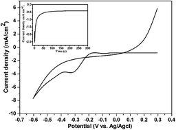
The compact nickel telluride (NiTe) thin film was prepared by two simple steps. High-density tellurium (Te) film with vertical pillar morphology (Te source) was synthesized by a rapid and convenient electrodeposition method without any external agent for the first time. NixTe as the ohmic contact layer material was obtained by a low temperature heat treatment of a Te thin film deposited on a Ni substrate. The structure, morphology, optical and electrical properties of the as-prepared thin films were examined. The current voltage (I–V) characteristic shows that all of the NixTe/Ni samples have already formed ohmic contacts. The NiTe/Ni also shows smaller contact resistance than other samples, which suggests it has potential for application in solar cells as a flexible Ni substrate.
Nickel telluride (NiTe), an important intermetallic compound with a nickel-arsenide-type (NiAs type) crystal structure, has attracted great interest because of its electric, magnetic, crystallographic (helical chain conformation) and thermodynamic properties.26–30 In 1938, Tengnér asserted the existence of a continuous solid-solution range between the compounds NiTe and NiTe2. He suggested that NiTe (NiAs type) was transformed to NiTe2 (Cd(OH)2 type).31 It is important to point out that NiTe can be used as an ohmic contacting layer of II–VI semiconductors used for their distinctive electrical transport property.32 Traditionally, the method used to prepare NiTe is the direct combination of the Ni and Te elements in evacuated silica tubes at high temperature (600 °C) for several hours.7 In addition, Zhang et al. have prepared NiTe nanocrystallites by a hydrothermal method with hydrazine hydrate as a reducing agent.33 Nevertheless, the previously mentioned methods for preparing NiTe have some disadvantages, such as toxicity, high energy consumption and relatively long reaction times. Thus, environmentally friendly, energy saving and convenient methods should be sought for commercial production.
In this work, a simple method to prepare NiTe was explored. Firstly, a simple one-step, environmentally friendly and template free electrochemical deposition method to deposit a Te thin film at room temperature without any external agent was used. Subsequently, the NiTe thin film was obtained by calcinating the as-prepared Te thin film (Te source) on a Ni substrate (Ni source) at 350 °C. It is worth mentioning that there are three advantages using this method to prepare chalcogenide compounds: (1) selection of a single Te source electrolyte avoids the complications involved with the codeposition of the elements and impurities, (2) using a graphite plate instead of a conventional platinum (Pt) as the counter electrode for Pt, the graphite may dissolve into the electrolyte and thus, influence the reaction of the working electrode,34 (3) compared to other research,35–38 crystalline products can be obtained by a thermal transformation step. Furthermore, the electrical properties of NiTe/Ni indicate that it would have a potential application as a back contacting layer in solar cells.
TeO32− + 6H+ + 4e− → Te + 3H2O |
The change of current density with time is shown in Fig. 1 (inset) during the direct current potentiostatic electrodeposition at −0.30 V (versus Ag/AgCl) for 300 s. It shows that the cathodic current density increases quickly initially and then decreases gradually. The change of current density within the initial 100 s corresponds to the Te nucleation on the Ni foil surface. During electrodeposition, the first process is fast ionization. Subsequently, the charge is redistributed under the action of the voltage. The current was reduced with the extension of the deposition time, which is attributed to the increases of the resistivity of the deposited film. After uniform nucleation is attained on the entire surface, the current density became constant and the film growth starts.
Fig. 2 shows the XRD pattern of the Te thin film on the Ni substrate. Besides the diffraction peaks from the Ni substrate denoted by the black solid circles, the peaks of the sample can be clearly observed at 27.57°, 38.24° and 45.96° as shown in Fig. 2, which can be indexed to the (101), (102), and (003) planes of the hexagonal phase Te (JCPDS card no. 36-1452). No other phase can be detected by XRD, which reveals that pure Te is obtained. In addition, the preferred orientation (101) and peaks with small full-width at half-maximum are indicative of good crystallization of the samples.
Fig. 3(a) and (b) show FESEM images of the sample, which reveals that the Ni substrate is covered with large-scale pillars, whose lengths range from 400 nm to 500 nm. They are oriented vertically with respect to the Ni substrate surface. The surface morphology of the as-deposited sample clearly shows that the pillars have a compact and uniform structure, and the surface is rough. The TEM image of a single pillar in Fig. 3(c) shows that the Te pillar has a diameter of 250 nm and a length of 500 nm. The SAED image taken from a single pillar further confirms the well-crystallized, hexagonal phase structure of the pillar (Fig. 3(d)). Regular diffraction dots show the single crystal nature of the Te pillar. Surveys of the sample using SAED indicate that these Te pillars are consistently the preferred orientation (101).
Fig. 3 (a) Cross-sectional FESEM image, (b) tilted top-view FESEM image, (c) TEM image of a single Te pillar and (d) SAED pattern of the sample. |
The UV-visible absorption spectrum for the as-deposited Te thin film is shown in Fig. 4. The UV-vis absorption bands are quite similar to those reported by Swan et al.40 and Qian et al.41 As shown in Fig. 4, there are two absorption peaks which are located at 248 nm and 563 nm. The absorption peak centered at 248 nm is because of the allowed direct transition from the valence band (p-bonding triplet) to the conduction band (p-antibonding triplet), and the other absorption peak at 563 nm can be assigned to a forbidden direction transition.39–41 However, further research is needed because the origin of this absorption peak is still not clear.42
Fig. 4 UV-visible absorption spectrum of a Te thin film fabricated with the electrochemical deposition method. |
To study the process of Te transformation into NixTe in detail, a series of experiments were carried out from 200 °C to 400 °C. Fig. 5 displays the XRD patterns of the as-prepared samples which were annealed from 200 °C to 400 °C for 30 min in N2. The results display the process whereby Te transforms into NiTe. As shown in Fig. 5, the phase transformation does not start when the annealing temperature is 200 °C. In addition, Fig. 5(c) shows that NiTe and Ni3Te2 appear with the disappearance of the Te phase when the Te film is sintered at 250 °C for 30 min. With increase of the annealing temperature, the diffraction peak intensity of NiTe changes, which indicates that the crystallinity has improved. At the same time, the diffraction peaks of Ni3Te2 weaken gradually until they disappear.
Fig. 5 XRD patterns of the samples prepared at different annealing temperatures for 30 min: (a) as-prepared Te, (b) 200 °C, (c) 250 °C, (d) 300 °C, (e) 350 °C, (f) 400 °C. |
The result of Fig. 5(e) indicates that the diffraction peak position and relative intensities of the prepared samples are well matched with the standard powder diffraction file NiTe (JCPDS 89-2018). No diffraction peaks from other products were surveyed. Furthermore, the NiTe completely transforms into (NiTe2 + Ni2.86Te2) when the annealing temperature is extended to 400 °C. In addition, the study of a series of annealing times at 350 °C is also carried out. Fig. 6 shows the XRD patterns of the samples prepared at 350 °C for different times (0–60 min). As shown in Fig. 6(b), the products are mainly Te and a mixture of some indistinct substances when the annealing time is 15 min. Fig. 6(c) shows that Te completely transforms into NiTe by extending the annealing time to 30 min. With increase of annealing time to 45 min and 60 min, the reaction products are mainly NiTe2 and a mixture of Ni2.86Te2. Above all, annealing temperature and time prompt the reaction and the phase transition. Therefore, the optimum reaction conditions should be (350 °C, 30 min) to make sure that the products prepared were pure phase and well-crystallized NiTe.
Fig. 6 XRD patterns of the samples prepared at 350 °C for different times: (a) as-prepared Te, (b) 15 min, (c) 30 min, (d) 45 min, (e) 60 min. |
As is known, NiTe can be obtained by hydrothermal and high temperature solid-state reactions,43,44 which require high energy consumption and relatively long reaction times. In contrast, the reaction temperature and time are only 350 °C and 30 min in this study. There may be interdiffusion of Ni and Te and solid-phase chemical reactions may occur. The reaction to form NiTe can be shown in the following equation:
Ni + Te → NiTe |
Based on the XRD result, a general trend of decreasing Ni content (Ni3Te2 → NiTe → NiTe2) with respect to the increase in annealing temperature can be observed. Thus, it suggests that as-generated NixTe may prevent further interdiffusion of Ni and Te, which is of benefit for photovoltaics because if too much metal diffuses out to the surface it can form defects and recombination centers.45 As shown in Fig. 5(f) and 6(d and e), the increased annealing temperature or prolonged annealing time results in samples that include two substances, NiTe2 and Ni2.86Te2. The reason for the appearance of Ni2.86Te2 may be because of some phase segregation but it needs to be investigated further.
The XRD, EDX and FESEM spectra of the NiTe thin film as as-deposited Te thin film are shown in Fig. 7. Fig. 7(a) and (b) show the cross-section and tilted top-surface FESEM images of the NiTe film, respectively. It is obvious that the morphology of NiTe is a dense thin film and the thickness is about 300 nm. Fig. 7(c) shows the XRD pattern of NiTe. All the diffraction peaks can be perfectly indexed to a pure hexagonal phase of NiTe (space group: P63/mmc), which is in good agreement with the standard XRD data (JCPDS 89-2018). The strong and sharp diffraction peaks indicate that the product is well crystallized. No peaks of impurities are detected, revealing that high purity NiTe films were fabricated in this experiment. In addition, NiTe has been peeled off from the Ni substrate before taking the EDX spectrum. As shown in Fig. 7(d), EDX analysis indicates that the sample is composed of Ni and Te and the atomic concentration of Ni and Te is 1.02 which is in agreement with the desired stoichiometric composition of NiTe. All of the results show that a NiTe thin film has been successfully prepared by simple calcination of a Te thin film deposited on a Ni substrate. According to the previous results, NiTe and Te are all hexagonal phase. In other words, the crystal structure has not changed during the transformation process.
Fig. 7 (a) Cross-sectional FESEM image, (b) tilted top-view FESEM image, (c) XRD and (d) EDX spectra of NiTe thin film. |
To characterize the conductive properties of the NixTe/Ni, the electrical contacts were made by attaching copper wires to the surface of the Te or NixTe films with colloidal silver paste as the conductive glue. The schematic diagram is shown in the inset of Fig. 8. Fig. 8 shows the room temperature I–V characteristic of the sample contacted on Ni. The linear I–V curves indicate ohmic contacts. And the slope of the I–V curve reveals electroconductivity. As shown in Fig. 8, electroconductivity is significantly improved by transforming Te into NixTe. When the annealing temperature is higher than 250 °C, all NixTe/Ni samples show linear I–V curves, indicating that ohmic contacts have already been formed on Ni. Furthermore, it is evident that the contact resistivity of sample NixTe/Ni firstly decreases and then increases with the increase of annealing temperature. It is well known that conductive properties depend on the materials. In our study, the heat treatment makes the material change (Te → Ni3Te2 → NiTe → NiTe2). It is reported that NiTe2 is suitable as a back contact layer for solar cells.46 The slope of the I–V curve of the sample NiTe/Ni is higher than other samples. The results verify that NiTe/Ni possesses better ohmic contact characteristics.
Fig. 8 Current voltage (I–V) curves of NixTe/Ni samples annealed at different temperatures. Inset: the structural schematic diagram of the electric properties measured. |
This journal is © The Royal Society of Chemistry 2014 |