A low-cost and rapid microfluidic paper-based analytical device fabrication method: flash foam stamp lithography

Yong He*ab, Yan Wuab, Xiao Xiaoab, JianZhong Fuab and GuangHuai Xueab
aThe State Key Lab of Fluid Power Transmission and Control, Department of Mechanical Engineering, Zhejiang University, Hangzhou 310027, China. E-mail: yongqin@zju.edu.cn
bZhejiang Province's Key Laboratory of 3D Printing Process and Equipment, Department of Mechanical Engineering, Zhejiang University, Hangzhou 310027, China

Received 25th September 2014 , Accepted 19th November 2014

First published on 19th November 2014


Abstract

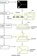
A novel and facile fabrication method of microfluidic paper-based analytical devices (μPADs) with flash foam stamp lithography (FFSL) is presented in this paper. First, a flash foam (also called photosensitive seal) stamp with desired patterns is made by flash exposing. Next, the stamp is immersed in a hydrophobic solvent such as polydimethylsiloxane (PDMS) to absorb the ink. Finally, the hydrophobic solvent is stamped on filter paper to form hydrophobic barriers. After the hydrophobic solvent cures, the μPAD is complete. Compared to common fabrication methods such as wax printing, inkjet printing, or direct writing, this paper will demonstrate that the FFSL method is convenient, quick, and cheap.


1. Introduction

μPADs, first proposed by Martinez et al.,1 have received plenty of attention from researchers due to their favorable potential application in disease diagnosis and biochemical analysis,2,3 as they possess many attractive features including usability, low cost, low consumption of reagents and samples, pumpless driving, portability, and disposability. Several methods have been used to fabricate μPADs, including photolithography,1,4,5 wax printing,6–8 inkjet printing,9–11 screen-printing,12,13 direct writing of PDMS,14 paper cutting,15,16 and others.

At first, Martinez et al. used SU-8 photoresist to make a hydrophobic port on papers.1 Haller et al.4 used a method of solventless initiated chemical vapor deposition to sedimentate photochromics on filter paper for UV lithography, then washed unreacted material to create μPADs. He et al.5 exposed the pre-hydrophobic filter paper to an octadecyltrichlorosilane (OTS) solution, then used UV mask photolithography to cause the irradiated areas to turn highly hydrophilic. μPADs fabricated by photolithography can acquire high resolution, however many materials used in photolithography isn't environmentally friendly.

Lu et al.6,7 and Carrilho et al.8 proposed a μPAD fabrication method based on wax printing. After using a spray wax printer to print the pattern of the hydrophobic region, they heated the paper until that wax could permeate it, creating μPADs with interphase hydrophilic and hydrophobic channels. Now this method is widely used in μPADs fabrication due to convenience and low cost. The wax might be attacked by organic solvents and the μPAD would be easily damaged due to bending and folding of paper.5

Fabricating μPADs with inkjet printing is another low cost method. Abe et al.9,10 soaked filter paper into a toluene solution with polystyrene. After the toluene volatilized, the filter paper became hydrophobic. They used inkjet printing to spray toluene solution onto the hydrophilic areas, then the toluene dissolved the polystyrene, creating μPADs. Li et al.11 printed AKD solution on filter paper, then dried the AKD solution to form hydrophobic areas, creating μPADs. The disadvantages of this method include the number of printing iterations required to dissolve the polystyrene, and the requirement of a modified printer. Its major advantage, conversely, is that it can sedimentate different chemical markers in different areas by printing many times.

Dungchai et al.12,13 used a screen-printing method to fabricate μPADs. In 2009, they reported the use of screen-printing to make the electrodes of μPADs, where they used traditional photolithography to make channels. In 2011, the team developed a wax screen-printing method. They sprayed wax onto a screen which was used as a mask, then dried it to create a wax barrier. The end result was a functional μPAD. The main disadvantage of this method is its low accuracy. The minimum widths of the hydrophilic channel and hydrophobic barrier are 600 μm and 1300 μm, respectively.

Bruzewicz et al.14 fabricated μPADs by using a direct writing method. They used a modified pen to extrude PDMS, then manipulated the pen in a two-dimensional motion to construct hydrophobic areas by plotting instrument. This method is very convenient but it is difficult to control the fabrication resolution.

Laser treatment and knife cutting are also reported to fabricate μPADs. Chitnis et al.15 processed hydrophilic channels on hydrophobic filter paper by laser. They sedimentated silica nanoparticles into the channels to realize the capillary drives of the hydrophilic channels. Fenton et al.16 deposited a regent on chromatography paper, then cut the filter paper to form hydrophilic channels by computer-controlled knife plotter. They then cut liquid inlets into cover tape to create μPADs. The main disadvantages of these methods are the high number of calibrations required, and its relatively low accuracy.

Various micro contact printing methods have been widely used to pattern polymers,17 biomolecules,18 and bacteria19 etc. on a variety of substrate. Although these methods could also be applied in producing μPADs, they are often expensive, and their resolutions are greater than that required for paper-based devices.20 Now some developments of fabricating μPADs with stamping have been reported as alternative methods in comparison to conventional techniques.20–22 Cheng et al.20 assembled a stamp with paper and tape, which can be used to pattern biochemical in paper. A PDMS high-relief stamp was used for replicate μPADs in chromatographic paper within 10 s by Curto et al.21 Zhang et al.22 reported how to fabricate an iron stamp and how to transfer wax to the paper surface with the stamp. As the above stamps are all not handheld, a lightweight stainless steel stamp was used to create paraffin barriers by Garcia et al.23 The above stamps reported were almost the hard stamp, so wax was commonly used as the hydrophobic barriers and this method may have the same shortage with wax printing. On the other hand, all the above stamps have low resolution, which means these fabrication methods are better suited for qualitative than quantitative work. Fabrication of μPADs with stamping is easy to operate, but different patterns of μPADs need different stamps, so finding low cost stamp is also necessary.

Flash foam stamp (FFS) is also called flash pre-inked stamp, or photosensitive seal stamp. When flash foam material is exposed to an intense burst of light, its micro-porous surface is sealed. If a masked area atop the flash foam is exposed, the pattern of the mask will be transferred to the flash foam, creating an FFS. Ink can then be stamped onto paper through the unsealed surface area of the FFS. Currently, FFS is commonly used to create personal stamps. It is favorable for this because it avoids the use of an inkpad, as the ink is stored in the micro-porous foam. Because FFS is already widely used in the fabrication of personal stamps, the process is quite cheap, and convenient.

In this paper, we propose a low-cost method of fabricating μPADs using FFS, called FFSL. With FFSL, only two steps are needed: the fabrication of the FFS, and stamping. A PDMS solvent was used as stamp ink, stamped on the filter paper to form hydrophobic barriers. After the solvent solidified, hydrophilic channels were formed between the hydrophobic barriers, and creating μPADs. All the materials used in FFSL are nontoxic, and the only specialized device required is a flash stamp machine. In addition, μPADs are easily bended and folded without damage as the hydrophobic barriers are formed by soft PDMS.

2. Materials and methods

2.1 Fabrication of FFS

The FFS and flash stamp machine were purchased from Liaocheng Beike Electronic Information Materials Co., Ltd. (Liaocheng, China) shown in Fig. 1a. The negative patterns of the μPADs were designed on the CorelDraw X4 (Corel Co., Ltd. Canada) then printed on tracing paper with an HP inkjet printer (600DPI) as the mask, shown in Fig. 1b. The flash foam, combined with the mask, is exposed in a flash stamp machine with xenon tubes, which delivers the intense burst of light that seals the non-printing area, or hydrophilic channels. A fine example of FFS is shown in Fig. 1c, where the dark area are the sealed micro holes, and the gray unsealed area is where stamp ink is stored for transfer to the paper during stamping.
image file: c4ra11150h-f1.tif
Fig. 1 Schema of fabrication of FFS (a) flash stamp machine; (b) mask pattern; (c) flash foam after exposed with mask.

Flash foam is a kind of ultra-micro bubble material, typically made by polyethylene, and the size of the microporous is very small and the average diameter is less than 30 microns, as shown in Fig. 2a and b. Due to microporous structures inside, the material itself has the characteristic of oil storage and permeation. Under strong light radiation, flash foam can absorb the light energy and transform it to heat energy. At the light exposure area, the surface of the flash foam instantly absorbs a great deal of energy and the temperature of flash foam quickly rises up to melting point. After the exposure, the temperature falls rapidly and the exposure area of flash foam forms a film, which has the function of porous sealing and isolation from the ink. This is the reason why FFS also called photosensitive seal stamp. As shown in Fig. 2c and d, the microporous are shrunk to close after exposition, from unsealed size of 20–30 μm to sealed size of 2–3 μm, so the ink could not passed through this area.


image file: c4ra11150h-f2.tif
Fig. 2 Micro structure of flash foam before and after exposure, before exposure (a) & (b), after exposure (c) & (d).

2.2 FFSL process

A typical FFSL process is shown in Fig. 3. First, an FFS with designed channels is fabricated, then immersed in hydrophobic solvent, in order to absorb ink, for about fifteen minutes. When the FFS is stamped onto the paper, the hydrophobic solvent transfers to the paper. μPADs with hydrophobic barriers are obtained after the hydrophobic solvent has solidified in a vacuum oven for about fifteen minutes in a temperature of 60 °C, or for an hour or so at room temperature.
image file: c4ra11150h-f3.tif
Fig. 3 Typical process of FFSL.

PDMS was chosen as the hydrophobic solvent, also used in the fabrication of μPADs with direct writing.14 PDMS part A and part B (Sylgard 184, Dow Corning) was mixed in a 10[thin space (1/6-em)]:[thin space (1/6-em)]1 (weight/weight) ratio and stirred for two minutes. The PDMS was then placed in vacuum desiccators for 10–13 minutes for degassing.

A μPAD fabricated by the FFSL method is shown in Fig. 4. When the PDMS solidified, the hydrophobic barrier area became semitransparent, as demonstrated in Fig. 4a. The contact angle of the hydrophobic barriers is about 120°, proving its favorable hydrophobic effect (Fig. 4b). Red ink can be absorbed and permeated from inlet to outlet at the hydrophilic area (Fig. 4c), demonstrating that the hydrophilic channel is interconnected well.


image file: c4ra11150h-f4.tif
Fig. 4 μPAD fabricated by FFSL method (a) after PDMS solidified; (b) ink in hydrophobic area with contact angle about 120°; (c) red ink absorbed by capillary action.

The resolution of μPADs fabricated by FFSL were assessed by testing how the minimal width of the hydrophilic channel and hydrophobic barrier are preserved when the μPAD is immersed in dye. The minimal width of the hydrophilic channel with complete submersion is defined as the resolution of the hydrophilic channel. Conversely, the minimal width of the hydrophobic barrier without submersion is defined as the resolution of the hydrophobic barrier. To determine the resolution of the FFSL method, the final widths of the hydrophobic barrier and hydrophilic channel were studied in the range of 50–1300 μm, with a design width of 50 μm, 100 μm, 200 μm, 300 μm, …, 1300 μm. Each barrier/channel in the FFS was repeated three times in the mask. After fabrication, the μPAD was immersed in red food dye for five seconds in order to visualize the hydrophobic and hydrophilic properties.

Quantitative analysis of NO2 was used to evaluate the performance of FFSL in performance analysis as a case study. Now this case has become a standard way to evaluate a new μPAD fabrication method. There are several reports about the NO2 analysis with μPADs.5,18–20 The detailed pattern and analysis method used in our case study can be found in ref. 5.

3. Results and discussion

3.1 Resolution of FFSL method

As shown in Fig. 5a, the hydrophilic channels between Group 1 and Group 5 weren't completely saturated by the dye, so the average width of the hydrophilic channels in Group 6 was the resolution for hydrophilic channels, with a measured width of 428 ± 21 μm, shown in Fig. 5a. The hydrophobic barriers in Group 1 and Group 2 were partly saturated, so the average width of the hydrophobic barriers in Group 3 was the resolution for hydrophobic barriers, with a measured width of 357 ± 28 μm, as shown in Fig. 5b.
image file: c4ra11150h-f5.tif
Fig. 5 Static resolution testing (a) hydrophilic channel testing; (b) hydrophobic barrier testing.

The resolution for hydrophilic channels of the μPADs fabricated by plotter printing was about 1000 μm, and the hydrophobic barriers was about 1000 μm (ref. 8) as well. The resolution for hydrophilic channels of the μPADs fabricated by screen-printing was 650 μm, and the hydrophobic barriers was 1300 μm.12 Compared to these two methods, the resolution of FFSL is more favorable.

3.2 FFSL cost & resolution analysis

The primary advantages of FFSL are its low cost and simplicity of operation. All the materials and instruments required are of low cost. The most expensive investment in FFSL manufacturing is the flash stamp machine, which is widely used to manufacture personal stamps and still only costs about %100. This machine is very compact, with a size of 320 mm × 170 mm × 170 mm, and conveniently portable, for when immediate fabrication of μPADs may be needed for an in-line field test. The other materials needed are listed in Table 1. The total cost of fabricating a piece of μPAD for the first time is only about fifteen cents (¥0.91/$0.15). As the FFS can be re-used to stamp several μPADs, the cost is much lower for subsequent μPADs.
Table 1 Cost of FFSL
Item Amount Cost
Filter paper 40 × 40 mm2 ¥0.15
Flash foam 40 × 40 mm2 ¥0.09
Tracing paper 40 × 40 mm2 ¥0.001
PDMS 0.5 g ¥0.4
Electric charge ≈0.1 kW h ¥0.05
Mask 1 piece of paper ¥0.01
Total ¥0.91/$0.15


The resolution of different μPADs fabrication methods of are listed in Table 2, although fabrication with photolithography and UV degradation & self-assembling layer have the highest resolution, the cost and the toxic material during the fabrication will restrict their wide use. The method of wax printing now is very popular and has a good resolution. The main instrument of wax printing is the wax printer, which is designed for replacement of inkjet and laser printer at the beginning. However, wax printer is completely defeated by inkjet printer and laser printer, and is seldom found in the office. If the wax printer is canceled by the manufacturer, how to fabricating μPADs with wax printing maybe a problem. FFSL can acquire almost the same resolution comparing with by inkjet printing, and don't need to customize any devices. Another low cost fabrication methods such as plotter printing of PDMS, wax screen-printing and knife cutting have low resolution, however FFSL can get a balance between cost and resolution.

Table 2 Comparison of μPADs fabrication methods
Method Channel (μm) Barrier (μm) Advantages Disadvantages
Photolithography1 186 ± 13 248 ± 13 High resolution Expensive device; complex fabrication
UV degradation & self-assembling layer5 233 ± 30 137 ± 21 High resolution; easy to fabricated Hydrophilic channels exposed to polymers or solvents
Wax printing8 561 ± 45 850 ± 50 Simple; suitable for mass-produce The design of the patterns must account for the spreading of the wax
Inkjet printing11 590 302 High resolution; rapid; low cost Requires a customized inkjet printer
Wax screen-printing12 650 ± 71 1300 ± 104 Easy to fabricated Low resolution
Plotter printing of PDMS14 ∼1000 ∼1000 Hydrophilic channels not exposed to polymers or solvents Low resolution; requires a customized plotter
Knife cutting24 2000 Low cost; rapid, can fabricate 3D μPADs Low resolution
FFSL 632 ± 27 306 ± 20 Low cost; rapid; flexible; environmentally friendly  


3.3 Complicated pattern fabrication

Some μPADs with more complicated channel patterns are fabricated to demonstrate the capability of FFSL method. Included examples are a Chinese map, Fig. 6a, logo of Zhejiang University, Fig. 6b, and dot array widely used in spotting, Fig. 6c, all successfully fabricated. The hydrophilic channels are well-preserved by hydrophobic barriers, allowing dye to diffuse to all hydrophilic channels. As shown here, the FFSL method performs well in the fabrication of many types of μPADs.
image file: c4ra11150h-f6.tif
Fig. 6 μPADs with complicated patterns, (a) Chinese map; (b) logo of Zhejiang University; (c) dot array.

3.4 Case study

To replicate this process, measure a concentration of NO2 for the sample according to the method described above. As shown in Fig. 7a, the concentrations of structural solution of NO2 in sample testing areas no. 1–7 are 0.3 mg L−1, 0.5 mg L−1, 1 mg L−1, 2 mg L−1, 3 mg L−1, 4 mg L−1, 5 mg L−1 in proper order, with a sample solution at a concentration of 1.8 mg L−1 in sample testing area no. 8. Transform Fig. 7a to grayscale by Adobe Photoshop, and draw a structure curve of the grayscale. The result of this is shown in Fig. 7b. The grayscale is proportional to the concentration, the regression equation of which is y = 5.9104x + 67.659 (where x represents the concentration of NO2 with a unit of mg L−1, and y represents the grayscale, which is dimensionless). According to the regression equation and the grayscale of the sample, we can calculate the concentration of NO2 in the sample solution, 1.75 mg L−1. The result agrees with the actual concentration of the sample, 1.8 mg L−1.
image file: c4ra11150h-f7.tif
Fig. 7 Quantitative analysis of NO2 (a) the analysis result of the concentration of NO2; (b) the linear relationship between the grayscale and the concentration of NO2.

3.5 Discussion

FFSL can be seen as a lightweight μPAD fabrication method with a middle resolution and a low cost, especially easy implementation. In this report, we just chose PDMS as the ink to stamp hydrophobic barriers, as this material is widely used in the analytical field. However, as a stamp method, various inks can be used to fabricate μPADs. Theoretically, any ink which will be solidified after stamp and keeps hydrophobic can used to form hydrophobic barriers, for example each type of ultraviolet (UV) resin. Compared with widely used μPAD fabrication method, such as wax printing and inkjet printing, FFSL provides an ability that researchers can design and choose suitable materials to form hydrophobic barriers according to different analytical environment.

4. Conclusion

A novel μPAD fabrication method, FFSL, was proposed. FFS, a method already widely used in the fabrication of personal stamps, is introduced for stamping μPADs. μPAD fabrication is simplified to two steps: FFS fabricating, and μPAD stamping. The process is incredibly simple to learn, and it is possible to fabricate flexible μPADs within 30 minutes, as the fabrication itself is very simple. Fabrication of FFS requires no toxic substances, which avoids the pollution of the environment, unlike photolithography. Furthermore, the only specialized instrument required is the flash stamp machine, which only costs about %100 and is lightweight and portable. Using FFSL, any lab can fabricate μPADs immediately and successfully in a cost-effective manner.

Acknowledgements

This paper is sponsored by the Science Fund for Creative Research Groups of National Natural Science Foundation of China (no. 51221004), National Natural Science Foundation of China (no. 51375440), Fundamental Research Funds for the Central Universities (no. 2013QNA4007), and Zhejiang Provincial Natural Science Foundation of China (no. LY12E05018).

References

  1. A. W. Martinez, S. T. Phillips and M. J. Butte, et al. Patterned paper as a platform for inexpensive, low-volume, portable bioassays, Angew. Chem., Int. Ed., 2007, 46(8), 1318–1320 CrossRef CAS PubMed.
  2. A. W. Martinez, S. T. Phillips and G. M. Whitesides, et al. Diagnostics for the developing world: microfluidic paper-based analytical devices, Anal. Chem., 2009, 82(1), 3–10 CrossRef PubMed.
  3. K. Yamada, S. Takaki and N. Komuro, et al. An antibody-free microfluidic paper-based analytical device for the determination of tear fluid lactoferrin by fluorescence sensitization of Tb3+, Analyst, 2014, 139(7), 1637–1643 RSC.
  4. P. D. Haller, C. A. Flowers and M. Gupta, Three-dimensional patterning of porous materials using vapor phase polymerization, Soft Matter, 2011, 7(6), 2428–2432 RSC.
  5. Q. He, C. Ma and X. Hu, et al. Method for fabrication of paper-based microfluidic devices by alkylsilane self-assembling and UV/O3-patterning, Anal. Chem., 2013, 85(3), 1327–1331 CrossRef CAS PubMed.
  6. Y. Lu, W. Shi and L. Jiang, et al. Rapid prototyping of paper-based microfluidics with wax for low-cost, portable bioassay, Electrophoresis, 2009, 30(9), 1497–1500 CrossRef CAS PubMed.
  7. Y. Lu, W. Shi and J. Qin, et al. Fabrication and characterization of paper-based microfluidics prepared in nitrocellulose membrane by wax printing, Anal. Chem., 2009, 82(1), 329–335 CrossRef PubMed.
  8. E. Carrilho, A. W. Martinez and G. M. Whitesides, Understanding wax printing: a simple micropatterning process for paper-based microfluidics, Anal. Chem., 2009, 81(16), 7091–7095 CrossRef CAS PubMed.
  9. K. Abe, K. Kotera and K. Suzuki, et al. Inkjet-printed paperfluidic immuno-chemical sensing device, Anal. Bioanal. Chem., 2010, 398(2), 885–893 CrossRef CAS PubMed.
  10. K. Abe, K. Suzuki and D. Citterio, Inkjet-printed microfluidic multianalyte chemical sensing paper, Anal. Chem., 2008, 80(18), 6928–6934 CrossRef CAS PubMed.
  11. X. Li, J. Tian and G. Garnier, et al. Fabrication of paper-based microfluidic sensors by printing, Colloids Surf., B, 2010, 76(2), 564–570 CrossRef CAS PubMed.
  12. W. Dungchai, O. Chailapakul and C. S. Henry, A low-cost, simple, and rapid fabrication method for paper-based microfluidics using wax screen-printing, Analyst, 2011, 136(1), 77–82 RSC.
  13. W. Dungchai, O. Chailapakul and C. S. Henry, Electrochemical detection for paper-based microfluidics, Anal. Chem., 2009, 81(14), 5821–5826 CrossRef CAS PubMed.
  14. D. A. Bruzewicz, M. Reches and G. M. Whitesides, Low-cost printing of poly(dimethylsiloxane) barriers to define microchannels in paper, Anal. Chem., 2008, 80(9), 3387–3392 CrossRef CAS PubMed.
  15. G. Chitnis, Z. Ding and C. L. Chang, et al. Laser-treated hydrophobic paper: an inexpensive microfluidic platform, Lab Chip, 2011, 11(6), 1161–1165 RSC.
  16. E. M. Fenton, M. R. Mascarenas and G. P. López, et al. Multiplex lateral-flow test strips fabricated by two-dimensional shaping, ACS Appl. Mater. Interfaces, 2008, 1(1), 124–129 CrossRef PubMed.
  17. G. Csucs, R. Michel and J. W. Lussi, et al. Microcontact printing of novel co-polymers in combination with proteins for cell-biological applications, Biomaterials, 2003, 24(10), 1713–1720 CrossRef CAS.
  18. I. Elloumi-Hannachi, M. Maeda and M. Yamato, et al. Portable microcontact printing device for cell culture, Biomaterials, 2010, 31(34), 8974–8979 CrossRef CAS PubMed.
  19. D. B. Weibel, A. Lee and M. Mayer, et al. Bacterial printing press that regenerates its ink: contact-printing bacteria using hydrogel stamps, Langmuir, 2005, 21(14), 6436–6442 CrossRef CAS PubMed.
  20. C. M. Cheng, A. D. Mazzeo and J. Gong, et al. Millimeter-scale contact printing of aqueous solutions using a stamp made out of paper and tape, Lab Chip, 2010, 10(23), 3201–3205 RSC.
  21. V. F. Curto, N. Lopez-Ruiz and L. F. Capitan-Vallvey, et al. Fast prototyping of paper-based microfluidic devices by contact stamping using indelible ink, RSC Adv., 2013, 3(41), 18811–18816 RSC.
  22. Y. Zhang, C. Zhou and J. Nie, et al. Equipment-free quantitative measurement for microfluidic paper-based analytical devices fabricated using the principles of movable-type printing, Anal. Chem., 2014, 86(4), 2005–2012 CrossRef CAS PubMed.
  23. D. T. P. Garcia, T. M. G. Cardoso and C. D. Garcia, et al. A handheld stamping process to fabricate microfluidic paper-based analytical devices with chemically modified surface for clinical assays, RSC Adv., 2014, 4(71), 37637–37644 RSC.
  24. P. K. Yuen and V. N. Goral, Low-cost rapid prototyping of flexible microfluidic devices using a desktop digital craft cutter, Lab Chip, 2010, 10(3), 384–387 RSC.

This journal is © The Royal Society of Chemistry 2014
Click here to see how this site uses Cookies. View our privacy policy here.