Specific features of electronic structures and nonlinear optical susceptibilities of superhard metallic diamond-like t-B2CN compound

A. H. Reshak*ab
aNew Technologies – Research Centre, University of West Bohemia, Univerzitni 8, 306 14 Pilsen, Czech Republic. E-mail: maalidph@yahoo.co.uk; Tel: +420 777729583
bCenter of Excellence Geopolymer and Green Technology, School of Material Engineering, University Malaysia Perlis, 01007 Kangar, Perlis, Malaysia

Received 15th September 2014 , Accepted 12th November 2014

First published on 13th November 2014


Abstract

The geometry of diamond-like t-B2CN was relaxed by minimizing the forces acting on each atom using an all-electron full potential linearized augmented plane wave within general gradient approximation (PBE-GGA). Using the relaxed geometry, the electronic band structure's dispersion, total and angular momentum resolved projected density of states, anthropomorphic shape of Fermi surface, electronic charge density distribution, and linear and nonlinear optical responses were performed within the local density approximation (CA-LDA), PBE-GGA, Engel–Vosko generalized gradient approximation (EV-GGA) and the modified Becke–Johnson potential (mBJ). Calculations showed that t-B2CN is metallic with two bands overlapping around the Fermi level. The density of states at the Fermi level N(EF) and the electronic specific heat coefficient (γ) were obtained. The electronic charge density showed that there are only two type of bonds (B–C and B–N). The Fermi surface is formed by two bands; the shape of the Fermi surface consists of empty areas representing holes and shaded areas corresponding to electrons. The linear optical response confirmed that there exists a lossless region between 5.0 eV and 7.5 eV, and the existence of a considerable anisotropy favors enhanced phase matching conditions for the second harmonic generation (SHG). The nonlinear optical susceptibilities exhibited that χ(2)113(ω) is the dominant component, with values of about 5.5 pm V−1 at static limit and 8.8 pm V−1 at λ = 1064 nm. This suggests that the t-B2CN single crystal is a promising nonlinear crystal in comparison with the well-known KTiOPO4 nonlinear optical single crystal.

1. Introduction

In recent years, combinations of superhard and metallic properties in multifunctional materials have been in great demand.1 Among these are boron–carbon–nitrogen compounds. These compounds possess short and strong 3D covalent bonds, making them superhard, superconducting materials.2 Several scientists have synthesized boron–carbon–nitrogen compounds using various methods.3–6 For example, BC6N, BC2N and B2CN, turbostratic, graphite-like and cubic structures have been synthesized using high temperature and high pressure,7–10 chemical vapor deposition (CVD),11–13 chemical synthesis14,15 and physical vapor deposition.16,17 As their band gaps can be adjusted (by changing compositions and atomic configurations), these compounds possess several electronic properties.18 The visible light emitting property makes BCN compounds useful for full color displays and optical storage;19 the negative electron affinity property makes them promising candidates for vacuum microelectronics and field emission flat displays.20

Previous work on BCN compounds has been devoted to crystal structure,2 electronic properties21 and the mechanical properties,22 with very few reports on linear optical properties.18 The lack of information regarding the electronic charge density distribution, Fermi surface and the linear and nonlinear optical properties for the superhard metallic diamond-like t-B2CN compound prompted us to perform comprehensive theoretical calculations based on density functional theory (DFT) within an all-electron full potential method. The calculations were performed using four exchange correlation potentials to ascertain the effect of exchange correlation on the electronic structure of the compound, and hence the linear and nonlinear optical properties. In these calculations, we employed a state-of-the-art all-electron full potential linear augmented plane wave (FPLAPW) method, which has proven to be one of the most accurate methods for computation of the electronic structure of solids within DFT.22–25

2. Details of calculations

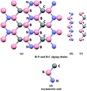
The t-B2CN crystallized in the tetragonal space group P-4m2 with one formula per unit cell; the structural parameters were a = 2.526 Å, b = 2.526 Å and c = 3.973 Å.2 In the unit cell, the B atom was situated at 2g (0.5 0.0 0.2701), C at 1b (0.5 0.5 0.0) and N at 1d (0.0 0.0 0.5). The geometry of t-B2CN was relaxed by minimizing the forces acting on each atom. We assumed that the structure was totally relaxed when the forces on each atom reached values less than 1 mRy per a.u. Calculations of geometrical relaxation were carried out using the generalized gradient approximation (PBE-GGA)26 within the state-of-the-art all-electron full potential linear augmented plane wave (FPLAPW) method as implemented in WIEN2k code.27 This is a density functional theory (DFT) implementation. The unit cell's geometry of t-B2CN is represented in Fig. 1; this contains four atoms and consists of B–C and B–N bonds, to form the hetero-diamond structure. Using the relaxed geometry, we calculated the ground state properties of t-B2CN. We used four types of exchange-correlation potentials. These are local density approximation (CA-LDA),28 PBE-GGA, Engel–Vosko generalized gradient approximation (EVGGA)29 and the recently modified Becke–Johnson potential (mBJ).30 It is well known that EVGGA can produce better exchange potential at the expense of less agreement in the exchange energy. This approach yields better band splitting compared with LDA and GGA, whereas mBJ use optimizes the corresponding potential for electronic band structure calculations. The weakness of the FPLAPW method lies in the strong dependence of the predicted properties on the chosen functional. As bench marking with experimental values was not possible because of the non-availability of pure samples of the material, the prediction of the optical susceptibility up to the third order is a bit risky.
image file: c4ra10480c-f1.tif
Fig. 1 (a) Fragment of the crystal structure of diamond-like t-B2CN compound; (b) B–N zigzag chain; (c) B–C zigzag chain; (d) asymmetric unit.

The plane-wave cutoff, defined by the product of the smallest atomic sphere radius times the magnitude of the largest reciprocal-lattice vector (RMT × Kmax), was taken to be equal to 8. In the muffin-tin (MT) spheres, the potential and charge density were expanded in spherical harmonics with lmax = 8 and nonspherical components up to lmax = 6. In the interstitial region, the potential and the charge density were represented by Fourier series. Self-consistency was obtained using 200 image file: c4ra10480c-t5.tif points in the irreducible Brillouin zone (IBZ). The electronic band structure, density of states, electronic charge density distribution, Fermi surface and the linear optical properties were calculated within 400 image file: c4ra10480c-t6.tif points in IBZ, while the nonlinear optical properties were calculated within 1200 image file: c4ra10480c-t7.tif points in IBZ. The self-consistent calculations were converged as the total energy of the system is stable within 0.00001 Ry.

3. Results and discussion

3.1. Electronic band structure, density of states and the electronic charge density

To investigate the contribution and the role of the four atoms in the hetero-diamond structure of t-B2CN, the electronic band structure along high symmetry points in first BZ was constructed using LDA, GGA, EVGGA and mBJ for seeking the best visualization and accurate results. The calculations show that there are small influences on the electronic band structure when the exchange correlation potentials are changed as illustrated in Fig. 2(a)–(d). The Fermi level (EF) was situated at 0.0 eV. In all cases there were only two bands cutting EF and forming the shape of the Fermi surface. To support this finding, the total and the angular momentum resolved projected density of states for t-B2CN compound were investigated as shown in Fig. 3(a)–(c). Fig. 3(a) shows that there are small influences on the density of states moving from LDA to GGA, EVGGA and mBJ. It is clear that the bands below −10.0 eV shift towards lower energy, while the bands above 4.0 eV shift towards higher energies. That is attributed to both EVGGA and mBJ exhibiting better band splitting than LDA and GGA. Therefore, we show the angular momentum resolved projected density of states (PDOS) obtained by mBJ. Fig. 3(b) and (c) allows us to visualize the angular momentum character of the various structures. It is clear that B-2s/p, C-2s/p and N-2s/p states overlapped around EF and the higher contribution comes from the C-2p state. This overlapping is strong enough to indicate that the metallic nature of the t-B2CN compound and the density of states at Fermi level N(EF) is determined by this overlapping. We calculated the values of N(EF) for the total and partial density of states using LDA, GGA, EVGGA and mBJ. These values are listed in Table 1, with the obtained values LDA > GGA > EVGGA > mBJ. The electronic specific heat coefficient (γ), which is function of N(EF), can be calculated using the expression image file: c4ra10480c-t1.tif, where kB is the Boltzmann constant. The calculated (γ) for the total and partial density of states are listed in Table 1, again showing the values of (γ) LDA > GGA > EVGGA > mBJ.
image file: c4ra10480c-f2.tif
Fig. 2 The calculated electronic band structure of a diamond-like t-B2CN compound using four exchange correlation potentials; (a) LDA; (b) GGA; (c) EVGGA; (d) mBJ.

image file: c4ra10480c-f3.tif
Fig. 3 (a) Calculated total density of states (states per eV per unit cell) using LDA, GGA, EVGGA and mBJ; (b and c) calculated partial density of states (states per eV per unit cell) B-s/p, C-s/p and N-s/p using mBJ.
Table 1 Calculated density of states at Fermi level N(EF) in (states/Ry/cell) for t-B2CN, B-s/p, C-s/p and N-s/p states along with the calculated electronic specific heat coefficient (γ) in (mJ mol−1 K2)
N(EF) LDA GGA EVGGA mBJ
N(EF)@B2CN 8.39 8.19 8.16 7.23
N(EF)@B-s 0.03 0.03 0.03 0.03
N(EF)@B-p 0.53 0.51 0.51 0.41
N(EF)@C-s 0.12 0.12 0.11 0.11
N(EF)@C-p 3.07 3.04 2.98 2.62
N(EF)@N-s 0.01 0.01 0.01 0.01
N(EF)@N-p 0.60 0.59 0.55 0.45
γ@B2CN 1.45 1.42 1.41 1.25
γ@B-s 0.01 0.01 0.01 0.00
γ@B-p 0.09 0.09 0.09 0.07
γ@C-s 0.02 0.02 0.02 0.02
γ@C-p 0.53 0.53 0.52 0.45
γ@N-s 0.00 0.00 0.00 0.00
γ@N-p 0.10 0.10 0.10 0.08


Fig. 3 suggests that DOS can be divided into two structures, the first extended between −15.0 eV and 2.0 eV, and the second structure extended from 4.0 eV and above. The first energy region is mainly formed by N-2p, C-2s/p states with small contributions from N-2s and B-2s/p states. The second region is formed by an admixture of C-2s/p, N-2s/p and B-2s/p states. There exists a strong hybridization between the states of B and C atoms, and also between B and N atoms resulting in B–C and B–N bonds. The calculated B–C bond length is 1.65 Å, which agrees well with previous theoretical results (1.63 Å),1 whereas B–N bond length is 1.55 Å, which also shows good agreement with previous theoretical results (1.54 Å).1 The calculated C–B–N bond angle is 112.29° and N–B–N is 108.25°, in very good agreement with previous results 112.0° (C–B–N) and 108.4° (N–B–N).1

The energy region extending from −10.0 eV up to Fermi level shows higher contribution for the N-2p state (0.6 electron per eV), C-2p (0.35 electron per eV), B-2p (0.11 electron per eV), B-2s (0.08 electron/eV), C-2s (0.05 electron per eV) and N-2s (0.02 electron per eV), confirming electron transformation from B-2s/p, N-2s/p and C-2s/p states to the valence bands and contribution in covalent interactions because of strong hybridization between the states.

The calculated electronic charge density distributions in the (1 0 1) and (1/2 0 0) crystallographic planes are represented in Fig. 4(a) and (b). It is clear that the (1 0 1) and (1/2 0 0) crystallographic planes represent B–N and B–C zigzag chains. There exist only two types of bonds: B–N and B–C bonds. It is well known that N atoms possess higher electro-negativity, 3.04, than both C (2.55) and B (2.04) atoms. The electro-negativity difference between B, C and N atoms causes the charge to be attracted towards N and C atoms, as shown by the blue (1.0000) color surrounding N and C atoms, which according to the charge density scale corresponds to the maximum charge accumulation site. The calculated electronic charge density distribution supported our previous finding on the partial density of states.


image file: c4ra10480c-f4.tif
Fig. 4 The electron charge density distributions were calculated for (a) (1 0 1) crystallographic plane showing B–N and B–C zigzag chains; (b) (1/2 0 0) crystallographic plane showing B–N and B–C zigzag chains.

3.2. Fermi surface

The calculated electronic band structure illustrates that there are two bands overlapped around the Fermi level along ΓZR, RRΓR and AΓ symmetry directions. These two bands form the shape of the Fermi surface of t-B2CN. The Fermi level is determined via the Kohn–Sham eigenvalue of the highest occupied state. The obtained shape of the Fermi surface is represented in Fig. 5(a)–(c). Fig. 5(a) and (b) shows that the Fermi surface is formed by bands # 7 and 8, from the partial density of states at the Fermi level, whereas Fig. 5(c) exhibits the shape of the Fermi surface, which consists of empty areas that represent holes, and shaded areas corresponding to electrons. At the center of BZ the Fermi surface is shaped from holes, whereas the Fermi surface in other symmetry directions is shaped from both holes and electrons. The shape of the Fermi surface helps to predict the magnetic, electrical, thermal and optical properties of the metallic and semimetallic materials.
image file: c4ra10480c-f5.tif
Fig. 5 Calculated Fermi surface (a) for band # 7; (b) for band # 8; (c) shape of Fermi surface.

3.3. Linear optical response

Calculations of optical dielectric functions involve the energy eigenvalues and electron wave functions, which are natural outputs of band structure calculations. The calculated electronic band structure and density of states confirmed the metallic nature of t-B2CN. Therefore, to calculate optical properties, we need to consider the intra-band transition (Drude term) in addition to the inter-band transitions as follows.31,32
 
εij2(ω) = εij2intra(ω) + εij2inter(ω) (1)
 
image file: c4ra10480c-t2.tif(2)
 
image file: c4ra10480c-t3.tif(3)
where m, e and are the electron mass, charge and Planck's constant, respectively. fc and fv represent the Fermi distributions of the conduction and valence bands, respectively. The term picv(k) denotes the momentum matrix element transition from the energy level c of the conduction band to the level v of the valence band at a certain k-point in the BZ, and V is the unit cell volume. τ is the mean free time between collisions, εkn is En(k) − EF, ϑijkn is the electron velocity and ωP is the anisotropic plasma frequency.33 The calculated values of ωxxP and ωzzP are listed in Table 2.
Table 2 The calculated ωxxP and ωzzP when εxx1(ω) and εzz1(ω) cross zero
xc ωxxP ωzzP
LDA 7.792 3.003
GGA 7.854 2.945
ECGGA 7.837 2.779
mBJ 8.312 2.383


The theoretical part of the optical dielectric function's dispersion for the tetragonal t-B2CN is εxx2(ω) = εyy2(ω) and εzz2(ω), therefore there are only two tensor components along the polarization directions [1 0 0] and [0 0 1] with respect to the crystalline axes. Thus, t-B2CN is a uniaxial crystal. Fig. 6(a) shows that at low energies there is a sharp rise in both εxx2(ω) and εzz2(ω), which is attributed to the inclusion of the Drude term (intra-band transitions) between B-2p, C-2p of the valence band and the two bands just above EF. Then after, a small peak appears at around 4.0 eV followed by a valley. At around 7.5 eV, both εxx2(ω) and εzz2(ω) exhibited a rapid increase to form the main peak which is situated between 10.0 and 13.0 eV. The observed peaks (10.0 to 13.0 eV) are caused by electric-dipole transitions between N-2p and C-2p of the VBs to B-2p of the CB. The εxx2(ω) component shows a considerable anisotropy with the εzz2(ω) component. From the theoretical part of the frequency-dependent dielectric functions, we can derive the actual parts with the aid of the Kramers–Kronig relations.32 These are εxx1(ω) and εzz1(ω), which are represented in Fig. 6(b). Again, this shows a sharp rise at low energies caused by intra-band transition (Drude term). There exists a considerable anisotropy between the two polarizations. We should emphasize that the considerable anisotropy in the linear optical response favors an enhanced phase matching conditions for the second harmonic generation (SHG). Using the real and theoretical parts of the optical dielectric functions, one can obtain the optical reflectivity, absorption coefficient, energy loss function and the optical conductivity. Fig. 6(c) illustrates the optical reflectivity as a function of photon energy. It is clear that the t-B2CN compound exhibits high reflectivity R(ω) at low energy, which is about unity. The first reflectivity minima for the two polarizations occur between 4.0 and 8.0 eV, confirming the occurrence of a collective plasmon resonance. The depth of the plasmon minimum is determined by the theoretical part of the frequency-dependent optical dielectric function at the plasma resonance, and is representative of the degree of overlap between the inter-band absorption regions. Then Rxx(ω) and Rzz(ω) show prompt increases to reach maximum reflectivity of about 80% at around 13.0 eV. The reflectivity spectra confirm the existence of the considerable anisotropy between the two polarization directions. The absorption coefficient of t-B2CN is represented in Fig. 6(d), which shows that there are two absorption bands, the first extended between 0.0 and 5.0 eV (low absorption region) and the second between 7.5 eV and 13.0 eV (high absorption region), in which the crystal exhibits high transparency. Therefore the region between 5.0 eV and 7.5 eV is a lossless region. Fig. 6(e) illustrates the loss function L(ω), which confirms the existence of the lossless region between 5.0 eV and 7.5 eV, in concordance with our observation in Fig. 6(d) and in agreement with previous work.18 The loss function's peaks represent the plasma frequencies (ωP). We should emphasize that above ωP the material behaves as dielectric where ε1(ω) is positive, while below ωP where ε1(ω) is negative the material exhibits metallic nature. The calculated theoretical and real parts of the optical conductivity dispersion Imσ(ω) and Reσ(ω) are shown in Fig. 6(f) and (g). Again, this shows the existence of the considerable anisotropy between σxx(ω) and σzz(ω), and the real part confirms the existence of the lossless region between 5.0 eV and 7.5 eV, which separates the two optical conductivity regions (0.0 up to 5.0 eV and 7.5 up to 13.0 eV). The optical conductivity is related to the frequency-dependent dielectric function ε(ω) as image file: c4ra10480c-t4.tif. The peaks in the optical conductivity spectra are determined by the electric-dipole transitions between the occupied states and the unoccupied states.


image file: c4ra10480c-f6.tif
Fig. 6 (a) Calculated εxx2(ω) (dark solid curve-black color online) and εzz2(ω) (light dashed curve-red color online) spectra. (b) Calculated εxx1(ω) (dark solid curve-black color online) and εzz1(ω) (light dashed curve-red color online) spectra. (c) Calculated Rxx(ω) (dark dashed curve-black color online) and Rzz(ω) (light solid curve-red color online). (d) Calculated absorption coefficient Ixx(ω) (dark solid curve-back color online) and Izz(ω) (light dashed curve-red color online) spectrum. The absorption coefficient in 104 s−1. (e) Calculated Lxx(ω) (dark solid curve-black color online) and Lzz(ω) (light dashed curve-red color online) spectrum. (f) Calculated Imσxx(ω) (dark solid curve-black color online) and Imσzz(ω) (light dashed curve-red color online) spectrum. (g) Calculated Reσxx(ω) (dark solid curve-black color online) and Reσzz(ω) (light dashed curve-red color online) spectrum.

3.4. Nonlinear optical response

As t-B2CN single crystals exhibit considerable anisotropy between the two polarization directions [1 0 0] and [0 0 1], therefore the anisotropy in the linear optical response favors enhanced phase matching conditions, which are necessary for generating the second harmonic. The tetragonal symmetry allows only four nonzero tensor components; these are the complex second-order nonlinear optical susceptibility tensors χ(2)113(ω), χ(2)232(ω), χ(2)311(ω) and χ(2)322(ω). The formulae of complex second-order nonlinear optical susceptibility tensors are given in ref. 34–36. For t-B2CN crystals, the χ(2)113(ω) = −χ(2)232(ω) and χ(2)311(ω) = −χ(2)322(ω) as illustrated in Fig. 7(a) and (b), which represent the dispersions of the theoretical parts of the χ(2)113(ω), χ(2)232(ω), χ(2)311(ω) and χ(2)322(ω) components. It is clear that χ(2)113(ω) and χ(2)232(ω) oscillated around zero, and each part of these two components shows the reverse part of the second component alternately, like a mirror. The same behavior is observed for χ(2)311(ω) and χ(2)322(ω) components. In Fig. 7(c), the absolute values of |χ(2)113(ω)| = −|χ(2)232(ω)| and |χ(2)311(ω)| = −|χ(2)322(ω)| are represented; as we take the absolute values of these components, one can see therefore |χ(2)113(ω)| = |χ(2)232(ω)| and |χ(2)311(ω)| = |χ(2)322(ω)|. This figure shows that the |χ(2)113(ω)| component has the highest value in comparison with the |χ(2)311(ω)| component. Thus |χ(2)113(ω)| is the dominant component, with a value of about 5.5 pm V−1 at static limit and 8.8 pm V−1 at λ = 1064 nm. This suggests that the t-B2CN single crystal is a promising NLO crystal in comparison with the experimental value of the well-known KTiOPO4 single crystal, which has a SHG value of about 1.19 ± 0.08 pm V−1 (ref. 37) and 1.91 ± 0.2 pm V−1 (ref. 38) for the |χ(2)113(ω)| component. Therefore, the static values of the second-order susceptibility tensors are very important and can be used to estimate their relative SHG efficiency. In our previous works,39–45 we calculated the linear and nonlinear optical susceptibilities using the FPLAPW method on several systems whose linear and nonlinear optical susceptibilities are known experimentally – in those previous calculations, we found very good agreement with the experimental data. Thus, we believe that the calculations reported in this paper would produce very accurate and reliable results.
image file: c4ra10480c-f7.tif
Fig. 7 (a) Calculated Imχ(2)113(ω) (dark solid curve-black color online) and Imχ(2)232(ω) (light long dashed curve-red color online) using mBJ. (b) Calculated Imχ(2)311(ω) (dark solid curve-black color online) and Imχ(2)322(ω) (light long dashed curve-red color online) using mBJ. (c) Calculated |χ(2)113(ω)| (dark solid curve-black color online) and |χ(2)311(ω)| (light long dashed curve-red color online) using mBJ.

4. Conclusions

We employed an all-electron full potential linearized augmented plane wave within LDA, GGA, EVGGA and mBJ to calculate some specific features of electronic structures, linear and nonlinear optical susceptibilities of a superhard metallic t-B2CN compound. The electronic band structure indicated that t-B2CN is a metallic compound. The density of states confirmed this funding, and the values of the density of states at Fermi level N(EF) and the electronic specific heat coefficient (γ) were reported. Calculations showed that t-B2CN possesses only two type of bonds. The Fermi surface was plotted and discussed. The electronic charge density confirmed that there are only two type of bonds (B–C and B–N). The linear and nonlinear optical responses were obtained based on the calculated band structure. The linear optical response exhibited a considerable anisotropy, which favors enhanced phase matching conditions for the second harmonic generation (SHG). The calculated SHG suggests that the t-B2CN single crystal is a promising NLO crystal in comparison with the well-known KTiOPO4 single crystal.

Acknowledgements

The result was developed within the CENTEM project, reg. no. CZ.1.05/2.1.00/03.0088, co-funded by the ERDF as part of the Ministry of Education, Youth and Sports OP RDI program. Computational resources were provided by MetaCentrum (LM2010005) and CERIT-SC (CZ.1.05/3.2.00/08.0144) infrastructures.

References

  1. J. L. He, L. C. Guo, E. Wu, X. G. Luo and Y. J. Tian, J. Phys.:Condens. Matter, 2004, 16, 8131 CrossRef CAS.
  2. Q. Li, D. Zhou, H. Wang, W. Chen, B. Wuc, Z. Wu and W. Zheng, Solid State Commun., 2012, 152, 71–75 CrossRef CAS PubMed.
  3. R. Riedel, J. Bill and G. Passing, Adv. Mater., 1991, 3, 551 CrossRef CAS.
  4. Y. Kusano, J. E. Evetts and I. M. Hutchings, Thin Solid Films, 1999, 344, 250 CrossRef.
  5. R. Sen, B. C. Satishkumar, A. Govindaraj, K. R. Harikumar, G. Raina, J. P. Zhang, A. K. Cheetham and C. N. R. Rao, Chem. Phys. Lett., 1998, 287, 671 CrossRef CAS.
  6. V. S. Teodorescu, A. Luches, R. Dinu, A. Zocco, M. F. Ciobanu, M. Martino, V. Sandu and M. Dinescu, Appl. Phys. A: Mater. Sci. Process., 1999, 69, S667 CrossRef CAS.
  7. J. L. He, Y. J. Tian, D. L. Yu, T. S. Wang, S. M. Liu, L. C. Guo, D. C. Li, X. P. Jia, L. X. Chen, G. T. Zou and O. Yanagisawa, Chem. Phys. Lett., 2001, 340, 431 CrossRef CAS.
  8. A. R. Badzian, Mater. Res. Bull., 1981, 16, 1385 CrossRef CAS.
  9. V. L. Solozhenko, D. Andrault, G. Fiquet, M. Mezouar and D. Rubie, Appl. Phys. Lett., 2001, 78, 1385 CrossRef CAS PubMed.
  10. S. Nakano, M. Akaishi, T. Sasaki and S. Yamaoka, Chem. Mater., 1994, 6, 2246 CrossRef CAS.
  11. A. R. Badzian, S. Appenheimer and T. Niemyski et al., Proceeding of the Third International Conference on CVD, ed. F. A. Glaski, American Nuclear Society, Salt Lake City, UT, April 1972, pp. 24–27, La Grange Park, IL Search PubMed.
  12. R. B. Kaner, J. Kouvetakis and C. E. Warble, et al., Mater. Res. Bull., 1987, 22, 399 CrossRef CAS.
  13. M. Kawaguchi, T. Kawashima and T. Nakajima, Chem. Mater., 1996, 8, 1197 CrossRef CAS.
  14. M. Hubacek and T. Sato, J. Solid Stat Chem., 1995, 114, 258 CrossRef CAS.
  15. R. Riedel, J. Bill and G. Passing, Adv. Mater, 1991, 3, 551 CrossRef CAS.
  16. M. Dinescu, A. Perrone and A. Caricato, et al., Appl. Surf. Sci., 1998, 692, 127 Search PubMed.
  17. S. Ulrich, H. Ehrhardt and T. Theel, et al., Diamond Relat. Mater., 1998, 7, 839 CrossRef CAS.
  18. J. Sun, H.-T. Wang, N.-B. Ming, J. He and Y. Tian, Apply. Phys. Lett., 2004, 84, 4544 CrossRef CAS PubMed.
  19. X. D. Bai, E. G. Wang, J. Yu and H. Yang, Appl. Phys. Lett., 2000, 77, 67 CrossRef CAS PubMed.
  20. T. Sugino and H. Hieda, Diamond Relat. Mater., 2000, 9, 1233 CrossRef CAS.
  21. W. Qing-Hua, H. Qian-Ku, L. Xiao-Guang, Y. Dong-Li, L. Dong-Chun and H. Ju-Long, Chin. Phys. Lett., 2007, 24, 180 CrossRef.
  22. F. M. Gao, J. L. He, E. D. Wu, S. M. Liu, D. L. Yu, D. C. Li, S. Y. Zhang and Y. J. Tian, Phys. Rev. Lett., 2003, 91, 015502 CrossRef.
  23. S. Gao, Comput. Phys. Commun., 2003, 153, 190 CrossRef CAS; K. Schwarz, J. Solid State Chem., 2003, 176, 319 CrossRef.
  24. A. H. Reshak, D. Stys, S. Auluck and I. V. Kityk, Phys. Chem. Chem. Phys., 2010, 12, 2975–2980 RSC.
  25. A. H. Reshak, D. Stys, S. Auluck and I. V. Kityk, Phys. Chem. Chem. Phys., 2011, 13, 2945–2952 RSC.
  26. J. P. Perdew, S. Burke and M. Ernzerhof, Phys. Rev. Lett., 1996, 77, 3865 CrossRef CAS.
  27. P. Blaha, K. Schwarz, G. K. H. Madsen, D. Kvasnicka and J. Luitz, WIEN2k, An augmented plane wave plus local orbitals program for calculating crystal properties, Vienna University of Technology, Austria, 2001 Search PubMed.
  28. W. Kohn and L. J. Sham, Phys. Rev. A, 1965, 140, 1133 CrossRef.
  29. E. Engel and S. H. Vosko, Phys. Rev. B: Condens. Matter Mater. Phys., 1993, 47, 13164 CrossRef.
  30. F. Tran and P. Blaha, Phys. Rev. Lett., 2009, 102, 226401 CrossRef.
  31. F. Bassani and G. P. Parravicini, Electronic States and Optical Transitions in Solids, Pergamon Press Ltd., Oxford, 1975, pp. 149–154 Search PubMed.
  32. F. Wooten, Optical properties of solids, Academic press, New York and London, 1972 Search PubMed.
  33. M. I. Kolinko, I. V. Kityk and A. S. Krochuk, J. Phys. Chem., 1992, 53, 1315–1320 CAS.
  34. S. Sharma, J. K. Dewhurst and C. Ambrosch-Draxl, Phys. Rev. B: Condens. Matter Mater. Phys., 2003, 67, 165332 CrossRef.
  35. A. H. Reshak, Ph.D. Thesis, Indian Institute of Technology-Rookee, India, 2005.
  36. S. N. Rashkeev and W. R. L. Lambrecht, Phys. Rev. B: Condens. Matter Mater. Phys., 2001, 63, 165212 CrossRef.
  37. L. K. Cheng, L. T. Cheng, J. Galperin, P. A. M. Hotsenpiller and J. D. J. Bierlein, J. Cryst. Growth, 1994, 137, 107 CrossRef CAS.
  38. H. Vanherzeele and J. D. Bierlein, Opt. Lett., 1992, 17, 982 CrossRef CAS.
  39. A. H. Reshak, V. Kityk and S. Auluck, J. Phys. Chem. B, 2010, 114, 16705–16712 CrossRef CAS PubMed.
  40. A. H. Reshak, S. Auluck and I. V. Kityk, J. Solid State Chem., 2008, 181, 789–795 CrossRef CAS PubMed.
  41. A. H. Reshak, S. Auluck and I. V. Kityk, J. Phys.: Condens. Matter, 2008, 20, 145209 CrossRef.
  42. A. H. Reshak, J. Chem. Phys., 2006, 124, 104707 CrossRef PubMed.
  43. A. H. Reshak, Eur. Phys. J. B, 2005, 47, 503–508 CrossRef CAS.
  44. A. H. Reshak, S. Auluck, D. Stys, I. V. Kityk, H. Kamarudin, J. Berdowski and Z. Tylczynskif, J. Mater. Chem., 2011, 21, 17219 RSC.
  45. A. H. Reshak, M. Piasecki, S. Auluck, I. V. Kityk, R. Khenata, B. Andriyevsky, C. Cobet, N. Esser, A. Majchrowski, M. S'wirkowicz, R. Diduszko and W. Szyrski, J. Phys. Chem. B, 2009, 113(46), 15237 CrossRef CAS PubMed.

This journal is © The Royal Society of Chemistry 2014
Click here to see how this site uses Cookies. View our privacy policy here.