
Spatially confined electric field effect for improved resistive switching behavior of a Ni/Ta-embedded TaOx/NiSi device†
Jingyu Parka,
Heeyoung Jeona,
Hyunjung Kima,
Woochool Jangb,
Hyungtak Seo*cd and
Hyeongtag Jeon*ab
aDepartment of Nano-scale Semiconductor Engineering, Hanyang University, Seoul 133-791, Korea. E-mail: hjeon@hanyang.ac.kr
bDivision of Materials Science and Engineering, Hanyang University, Seoul 133-791, Korea
cDepartment of Materials Science and Engineering, Ajou University, Suwon 443-739, Korea. E-mail: hseo@ajou.ac.kr
dDepartment of Energy Systems Research, Ajou University, Suwon 443-739, Korea
First published on 6th November 2014
Abstract
In this study, Ni/TaOx/NiSi and Ni/TaOx/Ta/TaOx/NiSi devices were fabricated, and the resistive switching (RS) behaviors were investigated. A 2 nm-thick Ta metal layer was deposited between two TaOx films to form a Ni/TaOx/Ta/TaOx/NiSi stack, which was analyzed using TEM. Based on a linear scale I–V curve and an R–V graph, both devices showed conventional bipolar conductive bridge random access memory (CBRAM) characteristics with formation/rupture of Ni conductive filaments (CFs). The Ta-embedded device showed lower forming/SET voltages and initial resistance due to the reduced effective thickness of TaOx films due to the inserted Ta metal layer. In addition, the Ta-embedded device exhibited improved endurance and resistance distribution due to suppression of the random formation of Ni CFs. In this study, Ni/TaOx/NiSi and Ni/TaOx/Ta/TaOx/NiSi devices were fabricated, and the resistive switching (RS) behaviors were investigated. A 2 nm-thick Ta metal layer was deposited between two TaOx films to form a Ni/TaOx/Ta/TaOx/NiSi stack, which was analyzed using TEM. Based on a linear scale I–V curve and an R–V graph, both devices showed conventional bipolar conductive bridge random access memory (CBRAM) characteristics with formation/rupture of Ni conductive filaments (CFs). The Ta-embedded device showed lower forming/SET voltages and initial resistance due to the reduced effective thickness of TaOx films due to the inserted Ta metal layer. In addition, the Ta-embedded device exhibited improved endurance and resistance distribution due to suppression of the random formation of Ni CFs.
Recently, interest in resistive switching memory (ReRAM) has extensively increased as a potential replacement for conventional charge-based memory devices, such as dynamic random access memory (DRAM) and flash memory beyond the 20 nm technology node, because of the simple structure, fast speed, and excellent scalability.1–3 The ReRAM device could be classified by the operation mechanism. One is anion based resistive switching memory or valence change memory (VCM). The other is cation based memory which commonly known as conductive bridge random access memory (CBRAM), programmable metallization cells (PMCs), and electrochemical metallization memory (ECM). The operation mechanism of VCM is mainly due to oxygen vacancy (Vo).4,5 The operation mechanism of CBRAM is formation and rupture of metallic conductive filaments (CFs) supplied by an active metal electrode. When a positive voltage is applied to an active electrode, active metal atoms are oxidized into metal ions, and they migrate to a cathode region (inert electrode). The migrated metal ions are reduced to metal atoms and form CFs, leading to switching from a high resistance state (HRS or off state) to a low resistance state (LRS or on state).6,7 Alternatively, when a negative bias is applied to an active metal, dissolution of metal CF occurs at the thinnest part of metal CF due to a highly focused electric field (usually occurring at active electrode). Metal atoms consisting of CFs are re-oxidized and re-deposited at the active electrode, which results in the switch back to HRS. Typically, Ag, Cu, and Ni metals are used as active electrodes due to their high diffusivity in the insulator (or solid electrolyte).2,8–11 In addition, various insulators have been studied for CBRAMs such as chalcogenides (GeSe,9 Cu2S12), oxides (SiO2,13 Ta2O5 (ref. 14 and 15)), and even polymer materials.16 However, random nucleation/growth properties of CF results in a large fluctuation of the on/off ratio and SET/RESET voltages (VSET and VRESET); these are considered major problems in the CBRAM device. Therefore, in order to improve characteristics of CBRAM, the CF nucleation sites should be controlled during repeated switching cycles. In recent reports, the location of CF could be directly controlled using metal nano-crystals and a metal layer-embedded system.17–19
In this study, the resistive switching (RS) characteristics and mechanism were investigated for a Ta-layer-embedded TaOx film compared to TaOx film without a Ta layer for the application of CBRAMs. Complementary metal oxide semiconductor (CMOS)-compatible materials, Ni, NiSi, and TaOx, were used as an active electrode, inert electrode, and switching insulator, respectively. By inserting the Ta metal layer in TaOx, the switching performance was significantly improved due to the stable nucleation/growth of CFs.
A 50 nm-thick Ni film was deposited on a hydrofluoric acid (HF)-cleaned, p-type Si wafer by an e-beam evaporator. The Ni film was then annealed using rapid thermal annealing (RTA) at 500 °C for 1 min under vacuum ambient for transformation to the NiSi phase. A 10 nm-thick TaOx film was deposited on the NiSi film using a radio frequency magnetron reactive sputter system at room temperature (RT) using a pure Ta metal target. The process pressure was 5 mTorr, and 300 W of plasma power was used. The flow rate of Ar and O2 gas was 20 and 10 sccm, respectively. Then, 2 nm-thick Ta film was deposited without a vacuum break with 10 sccm of Ar gas and 200 W of plasma power. A 10 nm-thick TaOx film was again deposited on the Ta/TaOx/NiSi using the same process mentioned above. A 20 nm-thick TaOx film without a Ta metal layer was deposited as the control sample. Thereafter, the Ni top electrode with a 200 μm diameter was deposited by an e-beam evaporator on TaOx/Ta/TaOx/NiSi and TaOx/NiSi film stacks using a shadow mask. The RS characteristics of fabricated Ni/TaOx/Ta/TaOx/NiSi and Ni/TaOx/NiSi devices were analyzed by an Agilent B1500A semiconductor parameter analyzer at RT. The devices were operated by DC voltage sweep mode, and the voltage was applied to the top electrode (Ni) with the bottom electrode grounded. A 10 mA current compliance (CC) was used for all the fabricated devices in order to prevent permanent breakdown. The device was measured by cross-sectional transmission electron microscopy (XTEM) and energy dispersive X-ray spectroscopy (EDX) in order to analyze device structure and composition of the interfacial layer.
Fig. 1(a) and (b) show XTEM images of Ni/TaOx/NiSi and Ni/TaOx/Ta/TaOx/NiSi devices, respectively. An approximately 20 nm-thick amorphous TaOx film was deposited on the NiSi bottom electrode as shown in Fig. 1(a). A 3 nm-thick interfacial layer was also formed between TaOx and the NiSi electrode. The composition of the interfacial layer was identified as NiSiOx using EDX line scan analysis (data not shown). In contrast, there was no observed interfacial layer between the Ni top electrode and TaOx film because the formation energy of 4/5Ta + O2 → 2/5Ta2O5 was much less than that of 2Ni + O2 → 2NiO over the entire temperature range.20
 | ||
| Fig. 1 XTEM images of (a) Ni/TaOx/NiSi and (b) Ni/TaOx/Ta/TaOx/NiSi CBRAM devices. | ||
Fig. 1(b) shows that the 25 nm-thick Ta-embedded TaOx film was deposited on the NiSi bottom electrode. A relatively uniform, ∼2 nm-thick Ta interlayer was deposited between the TaOx films. For the Ni/TaOx/NiSi device, the interfacial characteristics were similar to those of the Ni/TaOx/Ta/TaOx/NiSi device (i.e., no interfacial layer between the Ni electrode and TaOx films, and a 3 nm-thick interfacial layer was formed between the TaOx film and NiSi electrode).
Typical current–voltage (I–V) and resistance–voltage (R–V) plots of the Ni/TaOx/NiSi device are shown in Fig. 2(a) and (b), respectively. The pristine device required an electrical forming process at a 6.26 V forming voltage with 10 mA CC before device operation because TaOx film does not contain any Ni+ ions. During the forming process, Ni atoms in the top electrode were oxidized to Ni+ ions, resulting in localized doping in the TaOx film,21 which were swept to the bottom electrode by an applied electric field to form Ni CFs. The inset graph of Fig. 2(a) is the linear scale of the I–V curve. The voltage was first swept from 0 to 7 V to switch the device from the off state (HRS) to the on state (LRS) (i.e., SET process). The current increased abruptly at 5.5 V, the SET voltage (VSET). As shown in the inset of Fig. 2(a), the I–V hysteresis shows a linear behavior that indicates the device is operated by formation and rupture of Ni CFs. The VSET was smaller than the forming voltage because the localized doped Ni+ ions helped the Ni CFs grow easier compared to the forming process mentioned above. During the SET process, 10 mA CC was used to prevent permanent breakdown, as in the forming process. When the voltage was swept from 0 to −1.5 V, the current decreased significantly at −0.64 V, the RESET voltage (VRESET), and the device was switched to HRS. Fig. 2(b) shows the R–V curve obtained from Fig. 2(a). As the applied voltage increased from 0 to 5.5 V, the resistance of the device decreased gradually due to the gradual current increase resulting from vertical growth of the Ni CFs, whose shape was conical (i.e., a wide diameter at the bottom electrode and narrow diameter at the top electrode). Ni CF grows vertically by ion migration from the top electrode, leading to localized doped Ni+ ions in the TaOx film and sequential reduction to Ni atoms at the bottom electrode. When the vertically-grown Ni CF reached the top electrode, the resistance decreased abruptly at 5.5 V (SET process). In addition, when the voltage was swept back from 7 to 0 V, the resistance decreased slowly due to the lateral growth of Ni CFs (increased diameter of CF). The resistance of the device increased gradually as the voltage was swept from 0 to −0.64 V due to lateral dissolution of Ni CFs (decreased diameter of CF) due to electrochemical reaction. Ni CF was re-oxidized to Ni+ ions (especially near the top electrode), and these Ni+ ions from the CFs moved to the active top electrode and were reduced to Ni atoms combined to the Ni electrode. Finally, the resistance increased drastically at −0.64 V (RESET process) because the diameter of the Ni CFs at the top electrode region decreased to zero when Ni CF was detached from the top electrode. This is equivalent to the disruption of Ni CFs in the vicinity of the top electrode. Afterward, the resistance increased slowly due to vertical dissolution of Ni CFs. The proposed explanation is corroborated by the recently suggested CBRAM model.22 For the Ta-embedded TaOx device, the resistive switching behavior is nearly the same as that of the device without the Ta layer, as shown in Fig. 2(c) and (d) (the inset graph of Fig. 2(c) is a linear scale I–V curve, and the inset graph of Fig. 2(d) is the magnified graph range from 0 to 3 V). However, the forming voltage was 4.42 V, which was less than that in the device without the Ta layer. In addition, the VSET and initial resistance were also lower than in the device without the Ta layer, which was caused by the decreased effective oxide thickness due to the embedded Ta layer.18
 | ||
| Fig. 2 I–V hysteresis and R–V curves of the (a and b) Ni/TaOx/NiSi and (c and d) Ni/TaOx/Ta/TaOx/NiSi devices. The inset of ((a) and (c)) is a linear scale I–V hysteresis. The inset of (d) is a magnified graph ranging from 0 to 3 V. | ||
Fig. 3(a) and (b) show endurance data of devices without and with an embedded Ta layer, respectively. The read voltage was 0.1 V for both cases. The TaOx device without an embedded Ta layer exhibited a relatively large on/off ratio at >103 times. However, the device revealed unstable resistive switching behavior including repeated switching failure and recovery, as noted in the circled area of Fig. 3(a). This unstable switching could result from Vo. During TaOx film deposition, thin NiSiOx interfacial layer, which could have high defect density such as Vo, was formed as shown in Fig. 1. Therefore, operation mechanism of device is not only Ni+ ion but also Vo could play major role in CF formation. From the extracted I–V curve from continuous sweep, operation mechanism of device without Ta embedded layer is not just CBRAM (Formation/rupture of Ni CF). The operation mechanism could be categorized according to three. Some show conventional CBRAM device which operated by Ni CF. Other mechanism is combination of Ni CF and Vo. The others exhibit conventional VCM which operated by only Vo (see S1 in the ESI†). The competition of three mechanisms complicates device operation and results in degradation of device performance. On the other hands, the switching mechanism of Ta embedded device is conventional CBRAM (see S2 in the ESI†). The device was finally subject to permanent breakdown after 181 cycles. Alternatively, the device with an embedded Ta layer shows stable endurance up to 200 successive switching cycles with an on/off ratio of approximately 102, as shown in Fig. 3(b). The LRS values were similar to those in the device without an embedded Ta layer, while HRS values were much less than the device without the Ta layer because the embedded Ta layer reduced the effective thickness of the TaOx film, which results in a large current flow at HRS. In addition, the cumulative probability of each device is shown in Fig. 3(c) and (d). The Ta-embedded device exhibited much better resistance distribution for both LRS and HRS compared to that without Ta layer. Therefore, the substantial improvement in device characteristics was due to the embedded Ta layer in TaOx films. The inserted Ta metal layer may have changed the switching mechanism of the devices.
 | ||
| Fig. 3 Endurance data of the (a) Ni/TaOx/NiSi and (b) Ni/TaOx/Ta/TaOx/NiSi devices. Resistance distributions of the (c) Ni/TaOx/NiSi and (d) Ni/TaOx/Ta/TaOx/NiSi devices. | ||
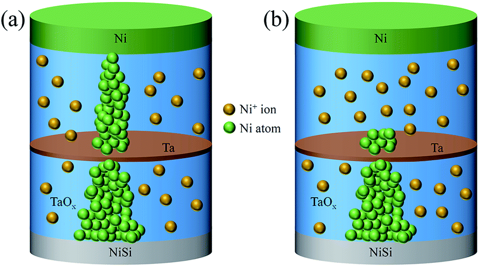
Fig. 4 shows a suggested switching mechanism of the Ta-embedded devices. After the forming/SET stage, the Ni top electrode dissolved into Ni ions, which resulted in localized doping in TaOx films and consecutive formation of CF, similar to the forming/SET process of the device without an embedded Ta layer, as shown in Fig. 4(a). The RESET process, however, was different from that of a single TaOx device due to the embedded Ta metal layer. The Ta-embedded device is regarded as a combination of two independent devices (device 1 is Ni/TaOx/Ta, and device 2 is Ta/TaOx/NiSi). Once Ni CF forms over the entire stack, the device turned on (switched from HRS to LRS). When negative voltage was applied to the top electrode, lateral dissolution occurred at the top of the Ni CFs because the high electric field was focused on the top.23 In particular, only the Ni CFs in device 1 were removed, while those in device 2 remained because of the electric field screening effect of the embedded Ta layer. The remaining Ni CF lead to increased current at HRS caused by a synergetic effect with decreased effective thickness due to the embedded Ta layer. In addition, the random formation of Ni CFs was suppressed when positive voltage was applied to the device because the electric field was locally focused on top of the remaining Ni CFs in device 2. Therefore, the location of newly formed Ni CFs was confined near the remaining Ni CFs in device 2, thus improving the resistive switching behavior of CBRAM.
 | ||
| Fig. 4 Schematic of the switching mechanism of the Ni/TaOx/Ta/TaOx/NiSi device after (a) SET and (b) RESET. | ||
Conclusions
In conclusion, the resistive switching behavior and mechanism of fabricated CBRAM devices consisting of Ni/TaOx/NiSi with an embedded Ta layer were investigated. The Ta-embedded TaOx device exhibited superior switching characteristics compared to the device without a Ta layer due to a modified switching mechanism. The Ta-embedded device is regarded as a combination of two devices (Ni/TaOx/Ta and Ta/TaOx/NiSi). During the forming process, Ni CF formed over the whole combined device. However, formation and rupture of Ni CFs occurred only in the Ni/TaOx/Ta region, while Ni CFs in Ta/TaOx/NiSi were unchanged by the applied bias due to the electric field screening effect of the embedded Ta layer. The random formation of Ni CFs can be suppressed by unchanged Ni CFs in the Ta/TaOx/NiSi region because the electric field is concentrated on top of the Ni. This study suggests that the insertion of a metal layer in an oxide channel can significantly improve the CBRAM performance by achieving better endurance and resistance distribution.Acknowledgements
This work was supported by a National Research Foundation (NRF) of Korea grant funded by the Korean government (NRF-2014M3A7B4049367) and (NRF-2014049368) through the NRF of MEST, Republic of Korea.Notes and references
- R. Waser and M. Aono, Nat. Mater., 2007, 6, 833 CrossRef CAS PubMed.
- R. Waser, R. Dittmann, G. Staikov and K. Szot, Adv. Mater., 2009, 21, 2632 CrossRef CAS.
- A. Sawa, Mater. Today, 2008, 11, 28 CrossRef CAS.
- D. Panda and T.-Y. Tseng, Thin Solid Films, 2013, 531, 1 CrossRef CAS PubMed.
- D. Panda and T.-Y. Tseng, J. Mater. Sci., 2013, 48, 4849 CrossRef.
- S. Menzel, S. Tappertzhofen, R. Waser and I. Valov, Phys. Chem. Chem. Phys., 2013, 15, 6945 RSC.
- S. Menzel, N. Adler, J. van den Hurk, S. Tappertzhofen, R. Waser and I. Valov, 5th IEEE International Memory Workshop (IMW), 2013, p. 92 Search PubMed.
- Y. Yang, P. Gao, S. Gaba, T. Chang, X. Pan and W. Lu, Nat. Commun., 2012, 3, 732 CrossRef PubMed.
- S. Z. Rahaman, S. Maikap, H.-C. Chiu, C.-H. Lin, T.-Y. Wu, Y.-S. Chen, P.-J. Tzeng, F. Chen, M.-J. Kao and M.-J. Tsai, Electrochem. Solid-State Lett., 2010, 13, H159 CrossRef CAS PubMed.
- K.-L. Lin, T.-H. Hou, Y.-J. Lee, J.-W. Chang, J.-H. Lin, J. Shieh, C.-T. Chou, T.-F. Lei, W.-H. Chang, W.-Y. Jang and C.-H. Lin, Jpn. J. Appl. Phys., 2013, 52, 031801 CrossRef.
- J. Sun, Q. Liu, H. Xie, X. Wu, F. Xu, T. Xu, S. Long, H. Lv, Y. Li, L. Sun and M. Liu, Appl. Phys. Lett., 2013, 102, 053502 CrossRef PubMed.
- T. Sakamoto, H. Sunamura, H. Kawaura, T. Hasegawa, T. Nakayama and M. Aono, Appl. Phys. Lett., 2003, 82, 3032 CrossRef CAS PubMed.
- Y. Bernard, V. T. Renard, P. Gonon and V. Jousseaume, Microelectron. Eng., 2011, 88, 814 CrossRef CAS PubMed.
- T. Tsuruoka, K. Terabe, T. Hasegawa and M. Aono, Nanotechnology, 2011, 22, 254013 CrossRef PubMed.
- Y. C. Yang, C. Chen, F. Zeng and F. Pan, J. Appl. Phys., 2010, 107, 093701 CrossRef PubMed.
- S. Gao, C. Song, C. Chen, F. Zeng and F. Pan, J. Phys. Chem. C, 2012, 116, 17955 CAS.
- Q. Liu, S. Long, H. Lv, W. Wang, J. Niu, Z. Huo, J. Chen and M. Liu, ACS Nano, 2010, 4, 6162 CrossRef CAS PubMed.
- D. Panda, C.-Y. Huang and T.-Y. Tseng, Appl. Phys. Lett., 2012, 100, 112901 CrossRef PubMed.
- D. Panda, A. Dhar and S. Ray, IEEE Trans. Nanotechnol., 2012, 11, 51 CrossRef.
- C. B. Lee, B. S. Kang, A. Benayad, M. J. Lee, S.-E. Ahn, K. H. Kim, G. Stefanovich, Y. Park and I. K. Yoo, Appl. Phys. Lett., 2008, 93, 042115 CrossRef PubMed.
- I. Valov and M. N. Kozicki, J. Phys. D: Appl. Phys., 2013, 46, 074005 CrossRef.
- S. Yu and H.-S. Philip Wong, IEEE Trans. Electron Devices, 2011, 58, 1352 CrossRef CAS.
- X. Guo, C. Schindler, S. Menzel and R. Waser, Appl. Phys. Lett., 2007, 91, 133513 CrossRef PubMed.
Footnote |
| † Electronic supplementary information (ESI) available. See DOI: 10.1039/c4ra10446c |
| This journal is © The Royal Society of Chemistry 2014 |