
Enhanced photoelectroctatlytic performance of etched 3C–SiC thin film for water splitting under visible light
Yazhou Wanga,
Sheng Lia,
Jisheng Hanb,
William Wena,
Hao Wangc,
Sima Dimitrijevb and
Shanqing Zhang*a
aCentre for Clean Environmental and Energy, Environmental Futures Research Institute, Griffith School of Environment, Griffith University, Gold Coast, QLD 4222, Australia. E-mail: s.zhang@griffith.edu.au
bQueensland Micro- and Nanotechnology Centre, Griffith University, Brisbane, QLD 4111, Australia
cThe College of Materials Science and Engineering, Beijing University of Technology, Beijing, 100124, P. R. China
First published on 17th October 2014
Abstract
3C–SiC films have robust mechanical and physicochemical properties and a narrow band gap (2.36 eV). In this work, a robust p-type 3C–SiC thin film is grown on a large silicon substrate using a low temperature alternating supply epitaxy method. The film is heavily doped with Al in order to achieve high conductivity and allow photoelectrocatalytic splitting of water for hydrogen production under visible light. The as-grown thin film is further treated with a facile dry etching process in order to improve the surface area and induce a light trap structure. In comparison with the as-grown sample, the etched thin film possesses substantially improved photoelectrocatalytic performance due to increased light absorption, larger surface area and reduced recombination rate of photoelectron and holes.
Introduction
The production of hydrogen via photoelectrocatalytic (PEC) splitting of water at a semiconductor surface has attracted tremendous research interest.1–4 SiC is a promising semiconductor for this application since SiC is chemically inert and resilient to chemical corrosion.5,6 Among common forms of SiC, 4H–SiC and 6H–SiC have large band gaps, i.e., 3.26 eV and 3.02 eV, respectively; therefore, they are not capable of utilizing visible light. In contrast, 3C–SiC processes a relatively narrower band gap (i.e., 2.36 eV), allowing it to absorb visible light.7,8 Also, it has a proper conduction band position, hence the photoelectrons can readily reduce H+ ions and produce H2. This attracts researchers' immediate attention and some remarkable outcomes for hydrogen revolution reaction using 3C–SiC nanocrystals have been achieved.9–11 However, the recycling of the SiC nanocrystals after the reaction involves time-consuming and costly processes. In fact, this becomes one of the major drawbacks of this technology. The use of robust and highly efficient 3C–SiC thin film on a substrate can tackle this recycling problem and make this technology economically viable.The 3C–SiC thin film is normally grown using low pressure chemical vapour deposition (LPCVD). The advantages of the thin film, such as high Young's modulus and toughness, chemical inertness, and radiation resistance, make it an excellent candidate for the fabrication of microelectromechanical systems (MEMS) devices that need to function at high temperature and in harsh environments. Conventionally, the growth of 3C–SiC are conducted at ca. 1350 °C,12–14 that is close to the melting point of Si (1414 °C). This readily causes thermal mismatch stress of the SiC film.15,16 In order to avoid the stress in SiC/Si heterostructure, eliminate the re-distribution of dopants in Si substrate and subsequently improve the uniformity and stability of the SiC film for the PEC splitting of water, we grew high quality single-crystalline 3C–SiC thin films on 8-inch Si wafters using alternating supply epitaxy (ASE) method at a much lower temperature i.e., 1000 °C.
Although the as-grown 3C–SiC thin film is suitable to be a catalytic electrode for water splitting with excellent stability, its surface is commonly extremely flat and highly reflective that decreases light absorption efficiency (see Fig. 1). In comparison with the as-grown thin film, the nano-size SiC particles illustrate a better PEC performance owing to its fast mass transport, rapid electron transfer and large surface area for light absorption.17 To apply the 3C–SiC thin film for water splitting application, these issues can be addressed by the following two strategies, i.e., the improvement of electronic conduction and the dramatic increase of surface area. Firstly, the improvement of the film conductivity in PEC process is able to ensure the photoelectron generated from the light absorption be shifted to external circuit immediately, which reduce the recombination of electron–hole pairs and improve the PEC efficiency (see Fig. 1). Secondly, the increase of surface area can provide more reaction sites for H+ reduction (see Fig. 1), which is beneficial to the PEC performance. Furthermore, this rough surface induced by the etched process might lead to the construction of light trapping structure (see Fig. 1b). The etched surface would provide additional mechanism for reflected photons to pass through the buck materials. As a result, the light absorption-path length is extended and absorption is increased.18,19
 | ||
| Fig. 1 Schematic illustration of light absorption and PEC production of H2 on the as-grown (a) and etched (b) 3C–SiC films. | ||
In order to realize these strategies, in this work, a highly conductive p-type single-crystalline Al doped 3C–SiC thin film is firstly produced by using a low temperature (i.e., 1000 °C) alternating supply epitaxy (ASE) method. This method could eliminate the re-distribution of dopants in Si substrate and subsequently improve the uniformity and stability of the SiC film. Secondly, a plasma dry-etch method is used to establish a rough surface morphology to facilitate large surface area and light absorption. Compared with the as-grown samples, the performance of the etched 3C–SiC thin film is evaluated in the process of PEC production of hydrogen.
Experimental
Preparation of p-type 3C–SiC
Al-doped 3C–SiC films with a thickness of 260 nm were grown on on-axis 8-inch Si (100) substrates in a specially designed LPCVD reactor with the ASE method using SiH4 (99.9999%), C2H2 (99.9999%) and trimethylaluminum (TMAL, 99.999%) as precursors. Epitaxy ready Si substrates were loaded into the LPCVD reactor.20,21 Then, the reactor temperature was ramped from 600 to 1000 °C at 5 °C min, and a flow of SiH4 at 1.5 SCCM (standard cubic centimeter per minute) was introduced to remove surface silicon dioxide of Si substrates. After that, the reactor temperature was cooled down to 750 °C to convert the Si substrate surface into SiC with a flow of C2H2 in a pressure of 0.05 mbar, followed by ramping the temperature up to 1000 °C under continuous flowing of hydrogen (H2), C2H2. Then the epitaxial growth of 3C–SiC was performed cycle by cycle using alternating supply epitaxy with SiH4, C2H2 and TMAL. The as-grown 3C–SiC thin film was etched by the Lam research etcher under the condition of 100 W power, 80 SCCM SF6 gas 120 mT pressure and 1.75 cm gap.Structural characterization
Structural analyses of the 3C–SiC thin film were performed using high-resolution X-ray diffractometer (XRD) with Cu-Kα radiations on a Bruker D8 System, scanning electron microscope (SEM) on JEOL JSM-7001F, and transmission electron microscopy (TEM) on cross-section specimens using a FEI Tecnai F30 TEM (operating at 300 kV). The surface morphology was observed by atomic force microscopy (AFM, model: MFP3D-BIO). Film thickness was measured by a NanoSpec profiler. The Al doping concentrations in the 3C–SiC films were measured by secondary ion mass spectroscopy (SIMS). The UV-vis diffusion reflectance (UV-vis) spectra were recorded by a UV-vis spectrometer (U3010, Hitachi) with an integrating sphere accessory.PEC characterization
In order to secure effective electrical contact, Ni was sputtered onto the electrical connection spot of the 3C–3C surface by Gamma 1000C sputtering system under the DC power 400 W in Ar at 50 SCCM. PEC experiments were carried out at 23 °C in a three-electrode PEC cell with a 3C–SiC thin film working electrode, a Ag/AgCl reference electrode, and a platinum mesh auxiliary electrode. The 3C–SiC thin-film working electrodes were mounted in a special holder with an area of 0.785 cm2 for visible light illumination. A 0.10 M NaNO3 solution was used as supporting electrolyte solution. A potentiostat (voltammograph, CV-27, BAS) was used to conduct linear sweep voltammetry (LSV) and amperometric measurement. The light source was a 150 W xenon lamp system (HFC-150, TrustTech). A visible light band pass filter (λ > 400 nm) was used to block the light in the UV region. Oriel Quantum Efficiency Measurement Kit was used to test Incident-Photon-to-Electron Conversion Efficiency (IPCE) of the thin film with interval wavelength of 1 nm. Electrochemical impedance spectroscopy (EIS) was carried out by CHI-660 with an amplitude of open-circuit voltage over the frequency range from 100 kHz to 0.01 Hz.Results and discussion
The as-grown 3C–SiC thin film is of high quality for electronic devices. Fig. 2 indicates that 3C–SiC film layer is compact and uniform with a thickness of ca. 260 nm. The inset of Fig. 2 shows a single-crystal diffraction pattern of the as-grown sample cross-section indicating that a parallel epitaxially grown film observed along the [110] direction of electron incidence complies with the Si substance. The etching process used in this work is a physical process that shall not affect the crystalline structure of the SiC film. As a matter of fact, significant difference was not observed between the as-grown and etched sample in TEM images. The TEM images indicate that the SiC/Si interface is well defined without obvious bubbles, stress or crack, which is stemmed from the proposed low temperature treatment method.20,21 This would be beneficial to its mechanical strength and chemical stability. | ||
| Fig. 2 TEM image and selected area electron diffraction (SAED) (inset). | ||
To enhance the PEC performance, the as-grown film is etched by the Lam research etcher to obtain a rougher surface. As shown in the XRD spectra in Fig. 3a, there is no obvious difference between the as-grown and etched samples after the etch treatment. A sharp distinctive diffraction peaks at ca. 41° of 2θ is corresponding to 3C–SiC (200) diffraction peak. A relatively strong diffraction peak at 69° is resulted from the diffraction of the Si (400) substrate and signal attenuation by the thin film. These results are indicating the fact that no other diffraction peaks are observed suggesting that the as-grown and etched samples are purely 3C–SiC single phase.22
 | ||
| Fig. 3 XRD spectra (a), SEM images and photos (inset) of the as-grown sample (b) and the etched sample (c). | ||
Fig. 3b and c are the SEM images illustrating the surface morphology of as-grown and etched films. Obviously, the surface of 3C–SiC films has a dramatical change after the etch treatment. The rough surface morphology is produced on the surface of the etched film by using the etch treatment from the extremely flat surface of as-grown film. Macroscopically, the surface of the as-grown sample is so smooth that it becomes as reflective as a mirror as shown in the inset of Fig. 3b (mirror image of Griffith University logo is clearly shown) while the reflective phenomenon is not observed for the etched sample as shown in the inset of Fig. 3c.
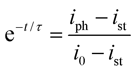
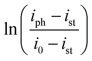
AFM images with roughness details of as-grown and etched samples are measured to further quantify the surface modifications after etch treatment. Apparently, the AFM results are in line with the SEM images observation in Fig. 4a and b, where the root mean squared surface roughness (Rrms) of the etched film (i.e., 14.9 nm) is substantially higher than that of the as-grown film (i.e., 8.8 nm). Roughness factor that represents the ratio of the actual surface area and projected surface area could illustrate the surface area enhanced by the etching process. The roughness factors of the as-grown and etched samples are 1.034 and 2.466, respectively. It suggests that the surface area of the etched film has been improved ca. 150% compared with the as-grown film. Overall, the etching process provides the thin-film a rough surface, that is the essential structure needed for light-trapping mechanism as shown in Fig. 1.18 UV-vis reflective spectra also suggest that the light absorption is dramatically enhanced by the etching process. For these specific 3C–SiC samples, the UV-Vis diffraction spectra in Fig. 4c show very significant oscillating behavior, which indicates the multiple reflections owing to the dramatic optical thin film interference from the refractive Si substrate. As a consequence, it is very difficult to quantify the light absorption and light reflection of the 3C–SiC thin films from the spectra. Nevertheless, we can safely conclude from Fig. 4c that the overall absorbance of the etched sample is much larger than that of the as-grown sample.
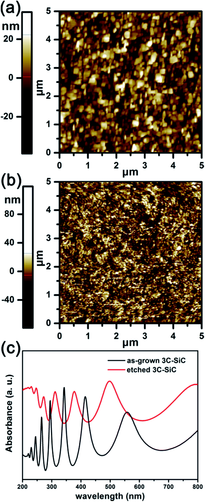 | ||
| Fig. 4 AFM images of the as-grown (a) and the etched samples (b) and the UV-vis spectra of as-grown and etched 3C–SiC films (c). | ||
Prior to the PEC experiment, nitrogen is sparged into the electrolyte solution to remove the dissolved O2 and avoid the side reaction of dissolved O2 (eqn (1))
| i.e., O2 + 2H2O + 4e− → 4OH− | (1) |
In the synthesis process, the Al dopant concentrations are controlled by the supplied amount of TMAl.24 The calculated average Al atomic concentrations of the as-grown 3C–SiC, 3C–SiC_b and 3C–SiC_a are in the range of 1.5 × 1020 cm−3, 3.9 × 1019 cm−3 and 1.6 × 1019 cm−3, respectively, while the corresponding resistances are determined to be 0.1 Ω cm, 0.31 Ω cm and 0.6 Ω cm, respectively. The photocurrent profiles under a visible light (1000 mW cm−2) with band pass filter (λ > 400 nm) of the as-grown thin films show in Fig. 5 clearly demonstrate that the photocurrent increases with the increase of dopant concentration. The as-grown film with highest Al density shows the lowest resistance and the best PEC performance.
 | ||
| Fig. 5 The photo-response profiles of various as-grown samples with different Al doping concentrations at 0 V potential under visible light. | ||
To further improve the PEC performance, we use dry etch method to modify the film surface of the as-grown sample and obtain the etched sample. As shown in Fig. 6a, in the dark, no currents are observed for both samples in the applied potential range of −0.2 and +0.2 V, while very weak reduction currents could be observed when the potential is more negative than −0.2 V. Under the visible light illumination (λ > 400 nm), the photocurrents are dramatically enhanced in comparison with the dark currents. Also, the etched sample exhibits much larger negative photocurrent than the as-grown sample. Interestingly, the onset potential of the etched sample (i.e., ∼−0.7 V) is lower than that of the as-grown sample (i.e., ∼−0.8 V). A more positive onset potential indicates a higher photoelectrocatalytic activity. This could be attributed to the enhancement of the light absorption and surface area, and more importantly, the creation of nanostructure at the surface could reduce the reaction energy barrier for the chemical reaction.25 This is coincide with the observation in the light on/off tests in Fig. 6b, where a constant potential of 0 V is applied because the electrochemical currents of the both samples are 0 under 0 V potential. The as-grown sample generates just a small photocurrent (4.6 μA cm−2), while a dramatically larger photocurrent (78.8 μA cm−2) is observed for the etched sample. This suggests that the PEC performance of the etched sample is about 17 times of that of the as-grown sample.
 | ||
| Fig. 6 The LSV of the as-grown and etched 3C–SiC films in the dark and under visible light at a scanning rate of 10 mV s−1 (a), photocurrent profiles at 0 V in the dark and under visible light (b), normalized plot of current–time dependence of the samples (c) and Nyquist curve of as-grown 3C–SiC and etched 3C–SiC films (d). | ||
Interestingly, when the light is turned on, a sharp photocurrent spike is observed (see Fig. 6b) due to the competitions between electron–hole recombination and electron consumption reaction (i.e., H+ reduction reaction for H2 production). When light is switched off, the flux of holes in the bulk and recombine with the photoelectron, resulting in the anodic current. A transient time constant (τ) can be calculated by analysing the transient photocurrent using kinetic equation,26,27
 | (2) |
 ) vs. time plot in Fig. 6c. τ values of the as-grown and etched samples are calculated as 0.32 s and 1.18 s, respectively. It is well-established that the magnitude of the τ value is inversely proportional to the extent of electron recombination.28 We conclude that the etching process could effectively reduce the recombination of electron–hole. Electrochemical impedance spectroscopy (EIS) measurements were performed to investigate the charge transfer resistance and the separation efficiency between the photogenerated electrons–holes and the RC time constants in Fig. 6d. These plots are best fitted by using the equivalent circuit shown in the inset of Fig. 6d. In our case, the RC time constants are obtained using electrochemical impedance spectrum (EIS) as shown are the same for both samples, i.e., 8.2 × 10⁻⁵ s. Therefore, for this particular system, the RC time constant will not affect our conclusion of the transient time constants of etched and as-grown samples. Nevertheless, the EIS results are strongly line with the analysis of transient photocurrents of as-grown and etched samples. It is demonstrated that the diameter of the semicircle observed for etched film is obviously smaller than as-grown film from the Nyquist plots of EIS data. The smaller arc radius of etched sample implies a higher efficiency of charge transfer in an electrochemical process.29 This result illustrates the photogenerated electron–hole pairs are more effectively separated in the etched SiC film.
The IPCE spectra of the as-grown and the etched films are collected under 0 V (vs. Ag/AgCl) as shown in Fig. 7a. The IPCE spectrum of the etched film shows a maximum value of ca. 23% at 500 nm, which is much higher than that of the as-grown film. Interestingly, the IPCE curves extend to 800 nm of the as-grown and etched SiC sample, which is ascribed to the p-Si substrate. Obviously, the IPCE values of the etched sample are higher than that of the as-grown sample throughout the entire wavelength range. The improvement of energy conversion efficiency by the etching process is attributed to the higher light absorption and lesser photo-generated electron–hole recombination. The results of IPCE spectra can further confirm the light trapping mechanism of the etched surface.
 | ||
| Fig. 7 IPCE spectra of the samples (a), the current–time plot of the samples with the data obtained from Fig. 3c at −0.8 V, the inset shows H2 appears at the SiC cathode while O2 at the Pt anode during PEC reaction (b). | ||
The current–time curve of the as-grown and etched samples as cathode for splitting water application with Pt gauze as anode at −0.8 V bias potential are shown in Fig. 7b. The inset of Fig. 7b, bubbles are noticeably observed at the surface of both cathode (etched sample) and anode (Pt gauze) after 5 and 50 min, respectively, suggesting the production of hydrogen gas at cathode and oxygen gas at anode. The slight fluctuation of the photocurrent of the etched SiC sample in Fig. 7b is very likely caused by the produced hydrogen bubbles at the SiC surface. The fact that no significant current drop and surface corrosion are observed after the tests suggests both thin films are chemically and electrochemically stable and larger photocurrent is produced at the etched sample. This is in line with more hydrogen gas are produced the etched sample due to the photocurrent is induced by the reduction of H+ ions.
Conclusions
In this work, a high quality single-crystalline p-type 3C–SiC thin film with excellent conductivity is produced. The etching treatment creates light trap structure and increases surface area of the thin film successfully. In comparison with the as-grown sample, the etched 3C–SiC film illustrates a better performance in PEC production of hydrogen due to three factors: the light trap structure for enhanced light absorption, reduced electron–hole recombination rate and boosted surface area for PEC reduction of H+ ions.Acknowledgements
The authors appreciate financial support from Australia Research Council and technical supports from Queensland Microtechnology Facility node of the Australian National Fabrication Facility (ANFF).Notes and references
- A. Fujishima and K. Honda, Nature, 1972, 238, 37–38 CrossRef CAS.
- Y. Liu, Y. Li, W. Li, S. Han and C. Liu, Appl. Surf. Sci., 2012, 258, 5038–5045 CrossRef CAS PubMed.
- M. J. Kenney, M. Gong, Y. Li, J. Z. Wu, J. Feng, M. Lanza and H. Dai, Science, 2013, 342, 836–840 CrossRef CAS PubMed.
- M. Gong, W. Zhou, M.-C. Tsai, J. Zhou, M. Guan, M.-C. Lin, B. Zhang, Y. Hu, D.-Y. Wang and J. Yang, Nat. Commun., 2014, 5, 4695 CrossRef PubMed.
- N. Mathews, Int. J. Hydrogen Energy, 2004, 29, 941–944 CrossRef CAS PubMed.
- Y. Y. Choi, J. G. Kim, S. J. Park and D. J. Choi, Chem. Phys. Lett., 2012, 531, 138–142 CrossRef CAS PubMed.
- D. H. van Dorp, N. Hijnen, M. Di Vece and J. J. Kelly, Angew. Chem., Int. Ed., 2009, 48, 6085–6088 CrossRef CAS PubMed.
- Y. Chen, X. Zhang, Q. Zhao, L. He, C. Huang and Z. Xie, Chem. Commun., 2011, 47, 6398–6400 RSC.
- C. He, X. Wu, J. Shen and P. K. Chu, Nano Lett., 2012, 12, 1545–1548 CrossRef CAS PubMed.
- M. Wang, J. Chen, X. Liao, Z. Liu, J. Zhang, L. Gao and Y. Li, Int. J. Hydrogen Energy, 2014, 39, 14581–14587 CrossRef CAS PubMed.
- H. Liu, G. She, L. Mu and W. Shi, Mater. Res. Bull., 2012, 47, 917–920 CrossRef CAS PubMed.
- M. Portail, M. Zielinski, T. Chassagne, S. Roy and M. Nemoz, J. Appl. Phys., 2009, 105, 083505–083507 CrossRef PubMed.
- M. A. Capano, B. C. Kim, A. R. Smith, E. P. Kvam, S. Tsoi and A. K. Ramdas, J. Appl. Phys., 2006, 100, 083514 CrossRef PubMed.
- H. Nagasawa, K. Yagi, T. Kawahara, N. Hatta and M. Abe, Microelectron. Eng., 2006, 83, 185–188 CrossRef CAS PubMed.
- M. Zielinski, A. Leycuras, S. Ndiaye and T. Chassagne, Appl. Phys. Lett., 2006, 89, 131906 CrossRef PubMed.
- J. Chen, J. Zhang, M. Wang, L. Gao and Y. Li, J. Alloys Compd., 2014, 605, 168–172 CrossRef CAS PubMed.
- J.-Y. Hao, Y.-Y. Wang, X.-L. Tong, G.-Q. Jin and X.-Y. Guo, Int. J. Hydrogen Energy, 2012, 37, 15038–15044 CrossRef CAS PubMed.
- S. Mokkapati and K. Catchpole, J. Appl. Phys., 2012, 112, 101101 CrossRef PubMed.
- C. He, X. Wu, J. Shen and P. K. Chu, Nano Lett., 2012, 12, 1545–1548 CrossRef CAS PubMed.
- J.-S. Han, S. Dimitrijev, F. Kong and A. Atanacio, J. Mater. Sci. Eng., 2009, 3, 15–17 Search PubMed.
- J. Han, P. Tanner, S. Dimitrijiev, Q. Shuang, Y. Shen and X. Xu, Mater. Sci. Forum, 2013, 1111–1114 CrossRef.
- L. Wang, S. Dimitrijev, J. Han, P. Tanner, A. Iacopi and L. Hold, J. Cryst. Growth, 2011, 329, 67–70 CrossRef CAS PubMed.
- K. Iwashina and A. Kudo, J. Am. Chem. Soc., 2011, 133, 13272–13275 CrossRef CAS PubMed.
- L. Wang, S. Dimitrijev, J. Han, P. Tanner, A. Iacopi and L. Hold, J. Cryst. Growth, 2011, 329, 67–70 CrossRef CAS PubMed.
- K. Zeng and D. Zhang, Prog. Energy Combust. Sci., 2010, 36, 307–326 CrossRef CAS PubMed.
- C. Y. Cummings, F. Marken, L. M. Peter, A. A. Tahir and K. G. U. Wijayantha, Chem. Commun., 2012, 48, 2027–2029 RSC.
- L. M. Peter and D. Vanmaekelbergh, in Advances in Electrochemical Science and Engineering, Wiley-VCH Verlag GmbH, 2008, pp. 77–163 Search PubMed.
- L. M. Peter, J. Li and R. Peat, J. Electroanal. Chem. Interfacial Electrochem., 1984, 165, 29–40 CrossRef CAS.
- X. Bai, L. Wang and Y. Zhu, ACS Catal., 2012, 2, 2769–2778 CrossRef CAS.
| This journal is © The Royal Society of Chemistry 2014 |