XRD and XPS studies of room temperature spontaneous interfacial reaction of CeO2 thin films on Si and Si3N4 substrates
Parthasarathi Bera* and
Chinnasamy Anandan
Surface Engineering Division, CSIR-National Aerospace Laboratories, Bangalore 560017, India. E-mail: partho@nal.res.in; Fax: +91-80-25210113; Tel: +91-80-25086359
First published on 24th October 2014
Abstract
X-ray diffraction (XRD) and X-ray photoelectron spectroscopy (XPS) investigations of interfacial reactions between Ce and Si have been carried out on the same set of as-deposited and 15 month aged films. XRD patterns demonstrate the presence of several peaks associated with CeO2 planes in aged CeO2/Si3N4 thin film in comparison with as-deposited nanocrystalline film, whereas the peak is broadened in the CeO2/Si film after aging. XPS studies show that interfacial reaction occurs spontaneously in CeO2/Si thin film at room temperature. Ce is present as both Ce4+ and Ce3+ oxidation states in as-deposited CeO2/Si thin film, whereas Ce4+ is the main species in CeO2 thin film deposited on the Si3N4 substrate. When XPS is recorded after 15 months, the concentration of Ce3+ species is observed to increase drastically in the CeO2/Si thin film. In contrast, interfacial reaction between the CeO2 and the Si3N4 substrate is not significant in the film even after 15 months of deposition. This shows that the initial room temperature spontaneous interfacial reaction observed in the CeO2/Si film continues at a much higher rate, whereas the nature of the CeO2/Si3N4 interface remains the same after 15 months, proving its stability.
1. Introduction
In the last few years, CeO2 based materials have attracted much attention for their applications in catalysis, hydrogen production, H2–O2 recombination in batteries and electrodes in fuel cells.1–5 In microelectronics, they have also been found to be high κ-gate oxide materials due to their unique properties like moderate band gap (3–3.6 eV), high dielectric constant (23–52), high refractive index (2.2–2.8) and high dielectric strength (∼25 MV cm−1).6 It is also suitable for Si based metal oxide semiconductor (MOS) devices due to its small lattice mismatch (−0.35%) with Si that favors its epitaxial growth on different silicon surfaces.6,7 In this regard, understanding of the growth, structure, nature of interface and long term stability between CeO2 and substrates are very crucial for device applications.CeO2 thin films have mainly been grown on Si, Si3N4, sapphire, LaAlO3, SrTiO3, glass, alloy and yttria-stabilized zirconia (YSZ) substrates using different thin film deposition techniques such as magnetron sputtering, electron beam evaporation, flash evaporation, pulsed laser deposition, ion beam epitaxy, molecular beam epitaxy, plasma enhanced chemical vapor deposition, sol-gel, spray pyrolysis have been employed to deposit CeO2 films.7–20 Recently, we have investigated interfacial reactions between CeO2 and substrates like Si, Al, Ti–6Al–4V alloy, Si3N4 and glass using XPS.8,9 It has been observed that significant interfacial reaction occurs between CeO2 and Si leading to the formation of Ce2O3 and silicate in CeO2/Si film, whereas reaction is limited in CeO2/Si3N4.8 Extent of interfacial reactions of CeO2 in different types of substrates are found as follows: Si > Al > Ti–6Al–4V alloy > Si3N4 > glass.9 However, reports on long term stability of CeO2/Si and CeO2/Si3N4 interfaces lack in the literature. In this communication, we compare the structural changes and reaction at the interfaces of CeO2/Si and CeO2/Si3N4 films after 15 months of deposition employing XRD and XPS.
2. Experimental methods
Details of growth and characterization of sputter deposited CeO2 thin films on Si and Si3N4 substrates are given in our previous publications.8,9 CeO2 thin films were deposited on Si and Si3N4 substrates of 10 mm × 10 mm × 0.6 mm dimensions using a CeO2 target (Allvac, 99.9%) employing magnetron sputtering assisted by inductively coupled plasma generated with 50 W RF power at 13.56 MHz. The substrates were cleaned with acetone and isopropyl alcohol with sonication prior to loading into the vacuum chamber. The chamber was pumped down to a base pressure of 3 × 10⁻⁶ mbar. The substrates were etched with H2 plasma prior to deposition of thin films. Sputter deposition was carried out at room temperature with Ar atmosphere at a pressure of 8 μbar. The substrate was biased to a constant negative voltage of 150 V and the target was biased with bipolar pulses of 300 V using a pulse generator. Thickness of obtained CeO2 thin films is around 25 nm. CeO2/Si and CeO2/Si3N4 thin films were kept in small plastic boxes in ambient conditions.The structures of as-deposited and aged CeO2 films were determined by XRD employing a PANalytical X'Pert PRO X-ray diffractometer operated with CuKα radiation of 1.5418 Å wavelength at 40 kV and 30 mA in the 2θ range 20–60° with step size of 0.033°. XPS of CeO2 thin films were recorded with a SPECS spectrometer using non-monochromatic AlKα radiation (1486.6 eV) as an X-ray source operated at 150 W (12.5 kV and 12 mA). The binding energies reported here were calculated with reference to C1s peak at 284.6 eV. All the spectra were obtained with pass energy of 25 eV and step increment of 0.05 eV. CasaXPS program was employed for curve-fitting of Ce3d core level spectra into several components with Gaussian–Lorentzian peaks after Shirley background subtraction. Peak positions, spin–orbit splitting, doublet intensity ratios and full width at half maximum (FWHM) were allowed to vary slightly as followed in the literature.
3. Results and discussion
XRD patterns of as-deposited and aged CeO2 thin films on Si and Si3N4 substrates are displayed in Fig. 1. Main diffraction peaks associated with substrates that appear after 60° are not shown here. In both as-deposited films, a broad peak observed at 33.4° corresponds to CeO2 (200) reflection (JCPDS no. 81-0792) indicating the nanocrystalline nature of the films.21 It is clear from the XRD patterns that CeO2 films grow preferentially to its (200) plane on Si and Si3N4 substrates. There is a significant change in the XRD pattern of aged CeO2/Si3N4 film. Intense diffraction peaks associated with (111), (200), (220) and (311) planes of CeO2 can be seen in the pattern of aged film. However, diffraction peak observed at 33.4° in as-deposited CeO2/Si film appears to be broad after 15 months of deposition.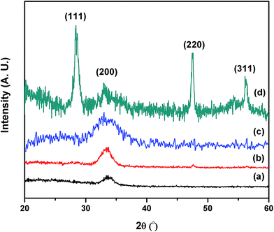 | ||
| Fig. 1 XRD patterns of (a) as-deposited CeO2/Si, (b) as-deposited CeO2/Si3N4, (c) aged CeO2/Si and (d) aged CeO2/Si3N4. | ||
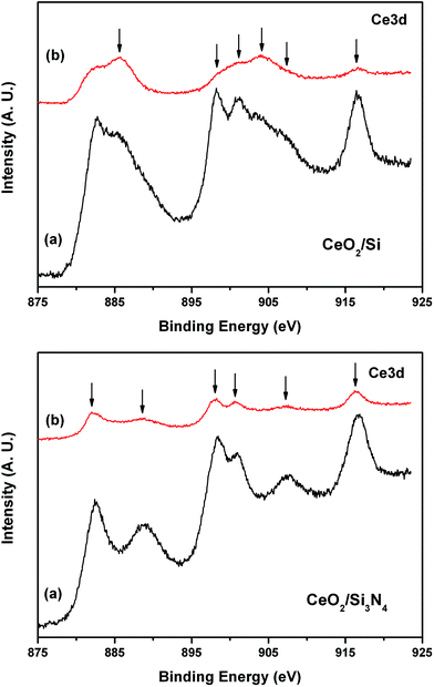
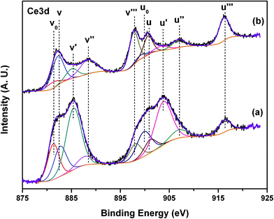
Ce3d core level spectra of CeO2/Si and CeO2/Si3N4 films at different conditions are shown in Fig. 2. It is clear from the figure that Ce3d spectral envelop of as-deposited CeO2/Si film is significantly different from the film after 15 months of deposition. Spectral envelops of the film deposited on Si substrate indicate that Ce is in both +4 and +3 oxidation states and it can be resolved into several Ce3d5/2,3/2 spin–orbit doublet peaks related to Ce4+ and Ce3+ species along with satellites. Satellite peaks are associated with the charge transfer from ligand (O2p) to metal (Ce4f) during photoionization processes. Appreciable change in Ce3d core level spectrum is observed in the aged CeO2/Si film. Comparison of spectral envelops indicates that most of Ce4+ species present in as-deposited film is transformed into Ce3+ species during this time span. In contrast, there is no appreciable change in the spectrum of CeO2/Si3N4 film after 15 months of deposition demonstrating that Ce is mostly present in +4 oxidation state. Fig. 3 presents typical curve-fitted Ce3d spectra of CeO2/Si and CeO2/Si3N4 films after 15 months of deposition. In both the figures, Ce3d spectra consist of 10 peaks that are curve-fitted in 5 doublets corresponding to 3d5/2 (labeled as v) and 3d3/2 (labeled as u) components. In curve-fitted Ce3d spectrum of CeO2/Si film, three doublet peaks labeled as v–u (882.7 and 901.2 eV), v′′–u′′ (888.8 and 907.1 eV) and v′′′–u′′′ (898.1 and 916.5 eV) with spin–orbit separation of 18.5, 18.3 and 18.4 eV, respectively are assigned for the Ce4+ species, whereas peaks labeled as vo–uo (881.6 and 899.6 eV) and v′–u′ (885.5 and 903.9 eV) are associated with Ce3+ species.8,9,22 The u′′′ peak is relatively well separated from the rest of the spectrum and is the characteristic of the presence of tetravalent Ce (Ce4+) in Ce compounds. It is to be noted that v′′′ and u′′′ spin–orbit peaks are attributed to the primary photoionization from Ce4+ with Ce3d94f0O2p6 final state, whereas lower binding energy peaks of v′′–u′′ and v–u correspond to the shake-down satellite features of Ce3d94f1O2p5 and Ce3d94f2O2p4 final states of Ce4+. Spin–orbit doublet peaks of v′–u′ are related to Ce3d94f1O2p6 final state of main photoionization from Ce3+ and associated lower binding energy vo–uo peaks are characteristic shake-down satellites of Ce3d94f2O2p5 final state. Peak areas (A) of Ce4+ and Ce3+ components are commonly used to estimate their relative concentrations (C) in the films using the following equations:8,23
| ACe3+ = Av0 + Au0 + Av′ + Au′ | (1) |
| ACe4+ = Av + Au + Av′′ + Au′′ + Av′′′ + Au′′′ | (2) |
 | (3) |
Concentration of Ce3+ in as-deposited CeO2/Si film is evaluated to be 32% with respect to the total amount of Ce species.8 On the other hand, mainly Ce3+ related peaks along with a small amount of Ce4+ can be seen in the film after 15 months of deposition and its concentration is 67% which is more than double in comparison with as-deposited film. In case of CeO2/Si3N4 film, Ce4+ species is predominant after 15 months of deposition. A comparison of concentrations of Ce4+ and Ce3+ evaluated from Ce3d spectra in CeO2/Si and CeO2/Si3N4 thin films at different conditions are given in Table 1. It is important to note that Ce3+ in CeO2/Si film can be related to the formation of cerium silicate or Ce2O3 at the interface.7 Drastic increase in the concentration of Ce3+ in CeO2/Si film compared to CeO2/Si3N4 film after 15 months of deposition indicates that interfacial reaction between CeO2 and Si occurs continuously in CeO2/Si film at room temperature.
| Ce species | As-deposited | Aged | ||
|---|---|---|---|---|
| CeO2/Si | CeO2/Si3N4 | CeO2/Si | CeO2/Si3N4 | |
| Ce4+ | 68 ± 1.73 | 89 ± 0.95 | 33 ± 4.4 | 82 ± 1.93 |
| Ce3+ | 32 ± 1.73 | 11 ± 0.95 | 67 ± 4.4 | 18 ± 1.93 |
O1s core level spectrum of respective CeO2 thin film can also reveal the oxidation states of Ce in the film. In Fig. 4, O1s core level spectra of CeO2/Si and CeO2/Si3N4 films at different conditions are shown. It is to be mentioned that O1s core level spectral envelop of as-deposited CeO2/Si film is different from that of aged film, whereas both spectra look similar in CeO2/Si3N4 film. Peak at 529.9 eV corresponds to O2− species in CeO2, whereas peak at 531.6 eV is associated with Ce3+ species originated from silicate or Ce2O3 species.8 It has been found from the figure that Ce4+ related peak along with strong peak associated with Ce3+ species are present in as-deposited CeO2/Si film. Intensity of the peak related to Ce4+ decreases drastically in the film after 15 months of deposition. On the other hand, intensity of the peak corresponding to Ce4+ remains unchanged in CeO2/Si3N4 film after 15 months of deposition.
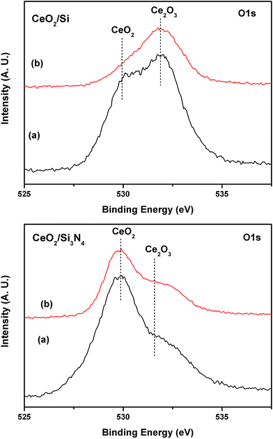 | ||
| Fig. 4 XPS of O1s core levels in CeO2 films deposited on Si and Si3N4 substrates: (a) as-deposited and (b) aged. | ||
High resolution Si2p core level spectra of CeO2/Si and CeO2/Si3N4 films at different conditions are shown in Fig. 5. Broad envelops of Si2p core level spectra in CeO2/Si films indicate the presence of elemental Si as well as oxidized Si species that can be curve-fitted into several component peaks. A peak at 99.3 eV is related to the contribution from elemental Si present in Si substrate. On the other hand, observed peaks at 101.2 and 102.4 eV correspond to Si2+ and Si3+ species, respectively.24,25 The appearance of these species at the interface of CeO2 and Si indicates the interaction between them resulting the formation of cerium silicate species.7,8 and concentrations of different oxide species increase in the film to some extent after 15 months of deposition demonstrating the continuous interfacial reaction over time. In contrast, a weak single peak at 101.5 eV in Si2p core level spectrum in CeO2/Si3N4 film is attributed to Si–N bond in Si3N4 and it remains same after 15 months of deposition.26
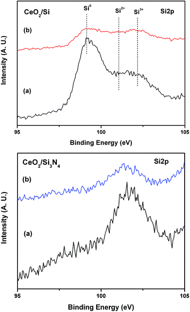 | ||
| Fig. 5 XPS of Si2p core levels in CeO2 films deposited on Si and Si3N4 substrates: (a) as-deposited and (b) aged. | ||
It has been observed from XPS studies that concentration of Ce4+ species in CeO2/Si film decreases after 15 months of deposition indicating the continuous reduction of Ce4+ species to Ce3+ at room temperature. Decrease in the u′′′ peak intensity and increase in v′ and u′ intensities in the film after 15 months of deposition confirms the Ce4+ reduction. On the other hand, Ce4+ species predominates in CeO2/Si3N4 film after 15 months of deposition demonstrating that CeO2/Si3N4 film is stable even after 15 months of deposition at room temperature. XRD results also support this finding as intense peaks related to CeO2 are observed only in CeO2/Si3N4 film indicating the lack of intermixing between CeO2 and Si in this system. Thus, spontaneous interfacial reaction at room temperature increases CeO2 reduction in CeO2/Si film. It has also been demonstrated earlier that interfacial reaction in CeO2/Si film can occur as change in standard molar free energy of formation of products and reactants (ΔG°) is negative (3Si + 8CeO2 → SiO + Si2O3 + 4Ce2O3, ΔG° = −340.8 kJ mol−1) indicating that reaction is thermodynamically favorable to proceed to their products.9 Therefore, this reaction continuously goes on at room temperature over the time.
4. Conclusions
CeO2 related prominent peaks are observed in XRD pattern of aged CeO2/Si3N4 film with respect to as-deposited film, whereas only peak observed in as-deposited film becomes broad in aged CeO2/Si film. XPS studies show that most of Ce4+ species gets reduced to Ce3+ in CeO2/Si film after 15 months of deposition, whereas mainly Ce4+ species is present in CeO2/Si3N4 film of same time period. Extent of spontaneous interfacial interaction at room temperature over time is found to be very high in CeO2/Si film, whereas it is significantly less in CeO2/Si3N4 film in the same condition. Thus, CeO2 film deposited on Si3N4 is stable in comparison with CeO2/Si film over time.Acknowledgements
Authors would like to thank the Director, CSIR-National Aerospace Laboratories for giving permission to publish this work.References
- A. Trovarelli, Catalysis by Ceria and Related Materials, Imperial College Press, London, 2002 Search PubMed.
- P. Bera and M. S. Hegde, J. Indian Inst. Sci., 2010, 90, 299 CAS.
- P. Bera and M. S. Hegde, Catal. Surv. Asia, 2011, 15, 181 CrossRef CAS.
- B. Hariprakash, P. Bera, S. K. Martha, S. A. Gaffoor, M. S. Hegde and A. K. Shukla, Electrochem. Solid-State Lett., 2001, 4, A23 CrossRef CAS PubMed.
- V. Matolín, M. Cabala, I. Matolínová, M. Škoda, M. Václavů, K. C. Prince, T. Skála, T. Mori, H. Yoshikawa, Y. Tamashita, S. Udea and K. Kobayashi, Fuel Cells, 2010, 10, 139 Search PubMed.
- W.-H. Kim, W. J. Maeng, M.-K. Kim, J. Gatineau and H. Kim, J. Electrochem. Soc., 2011, 158, G217 CrossRef CAS PubMed.
- F. Pagliuca, P. Luches and S. Valeri, Surf. Sci., 2013, 607, 164 CrossRef CAS PubMed.
- C. Anandan and P. Bera, Appl. Surf. Sci., 2013, 283, 297 CrossRef CAS PubMed.
- P. Bera and C. Anandan, Surf. Rev. Lett., 2014, 21, 1450054 CrossRef.
- I. Porqueras, C. Person, C. Corbella, M. Vives, A. Pinyol and E. Bertran, Solid State Ionics, 2003, 165, 131 CrossRef CAS PubMed.
- A. Ramírez-Duverger, A. R. Ruiz-Salvador, M. P. Hernández-Sánchez, M. F. García-Sánchez and G. Rodríguez-Gattorno, Solid State Ionics, 1997, 96, 89 CrossRef.
- G. Balakrishnan, C. M. Raghavan, C. Ghosh, R. Divakar, E. Mohandas, J. I. Song, S. I. Bae and T. G. Kim, Ceram. Int., 2013, 39, 8327 CrossRef CAS PubMed.
- A. G. Perez-Bergquist, Y. Zhang, T. Varga, S. Moll, F. Namavar and W. J. Weber, Nucl. Instrum. Methods Phys. Res., Sect. B, 2014, 325, 66 CrossRef CAS PubMed.
- J. T. Jones, E. T. Croke, C. M. Garland, O. J. Marsh and T. C. McGill, J. Vac. Sci. Technol., B: Microelectron. Nanometer Struct., 1998, 16, 2686 CrossRef CAS.
- D. Barreca, G. Bruno, A. Gasparotto, M. Losurdo and E. Tondello, Mater. Sci. Eng., C, 2003, 23, 1013 CrossRef PubMed.
- N. Özer, Sol. Energy Mater. Sol. Cells, 2001, 68, 391 CrossRef.
- R. Suresh, V. Ponnuswamya, R. Mariappan and N. S. Kumar, Ceram. Int., 2014, 40, 437 CrossRef CAS PubMed.
- S. B. Brachetti-Sibaja, M. A. Domínguez-Crespo, S. E. Rodil and A. M. Torres-Huerta, J. Alloys Compd., 2014, 615, 5437 CrossRef PubMed.
- Z. Jun, W. Feng, Y. Zhimin, C. Qiuyun, C. Jun and W. Shuming, J. Rare Earths, 2013, 31, 1191 CrossRef.
- Y. Zhang, F. Feng, H. Rongxia, K. Shi, S. Xiao, W. Wu, T. Qu, X. Wang and Z. Han, Curr. Appl. Phys., 2014, 14, 275 CrossRef PubMed.
- C. O. Avellaneda, M. A. C. Berton and L. O. S. Bulhões, Sol. Energy Mater. Sol. Cells, 2008, 92, 240 CrossRef CAS PubMed.
- J. M. Sánchez-Amaya, G. Blanco, F. J. Garcia-Garcia, M. Bethencourt and F. J. Botana, Surf. Coat. Technol., 2012, 213, 105 CrossRef PubMed.
- E. J. Preisler, O. J. Marsh, R. A. Beach and T. C. McGill, J. Vac. Sci. Technol., B, 2001, 19, 1611 CAS.
- J. R. Shallenberger, J. Vac. Sci. Technol., A, 1996, 14, 693 CAS.
- T. Skála and V. Matolín, Appl. Surf. Sci., 2013, 265, 817 CrossRef PubMed.
- S. I. Raider, R. Flitsch, J. A. Aboaf and W. A. Pliskin, J. Electrochem. Soc., 1976, 123, 560 CrossRef CAS PubMed.
| This journal is © The Royal Society of Chemistry 2014 |

