
Synthesis of porous microspheres composed of graphitized carbon@amorphous silicon/carbon layers as high performance anode materials for Li-ion batteries
Zailei Zhang*a,
Yanhong Wanga,
Wenfeng Rena,
Ziyi Zhongb and
Fabing Su*a
aState Key Laboratory of Multiphase Complex Systems, Institute of Process Engineering, Chinese Academy of Sciences, Beijing, 100190, China. E-mail: zhangzl@ipe.ac.cn; fbsu@ipe.ac.cn; Fax: +86-10-82544851; Tel: +86-10-82544850
bInstitute of Chemical Engineering and Sciences, A*star, 1 Pesek Road, Jurong Island, 627833, Singapore
First published on 21st October 2014
Abstract
We report in situ growth of amorphous silicon/carbon (Si/C) layers on graphitized carbon black (GCB) particles in porous microspheres (PMs) for formation of novel GCB@Si/C PMs as high performance anode materials. The preparation included spray drying, KOH activation and chemical vapor deposition at 900 °C, and used methyltrichlorosilane as both the Si and C precursor, which is a cheap byproduct in the organosilane industry. The obtained samples were characterized by X-ray diffraction, thermogravimetric analysis, nitrogen adsorption, transmission electron microscopy, and scanning electron microscopy. Compared with the bare GCB PMs, the GCB@Si/C PMs showed a significantly enhanced electrochemical performance with high lithium storage capacity and excellent cycling stability (the discharge capacity of GCB@Si/C-3 PMs and GCB@Si/C-6 PMs is maintained at 587.2 and 729.7 mA h g−1 after 200 cycles at a current density of 100 mA g−1), because the unique interconnected porous structure within the microspheres could absorb a large portion of Si volume change during Li insertion and extraction reactions, promote the diffusion of Li-ion and electrolyte solution, hinder the cracking or crumbling of the electrode, and additionally, the GCB and amorphous C provide high conductive electron pathway. This work opens a new way for fabrication of Si/C nanocomposites as anode materials for Li-ion batteries.
1. Introduction
Developing advanced lithium-ion batteries (LIBs) with high energy density, high rate capability and excellent cycling performance is crucial to electric vehicles, portable electronics and energy storage for many types of renewable energy sources.1–5 From the viewpoint of materials science, silicon (Si) is one of the most promising anode materials for LIBs due to its abundance in nature, relatively low working potential, and highest known theoretical capacity of 4200 mA h g−1 that is several times higher than that of the commercialized graphite.6,7 However, Si anodes are susceptible to rapid degradation because of the large volume changes (up to 300%) during lithiation and delithiation processes, formation of a thick solid–electrolyte interphase at the Si surface caused by the repeated volume changes, and the much lower conductivity of Si compared with the carbon anodes.8–11It has reported that nanostructured Si with specific morphologies such as nanowires,12–14 nanotubes,15–17 nanospheres,18 and nanoparticles19 can buffer the stress and strain effects caused by the particle volume expansion/contraction during the Li-ion insertion/extraction,20 and nanostructured Si/C composites can also prevent Si nanoparticle aggregation, enhance the conductivity and alleviate the volume change of Si, thus improving the cycling and rate capability.21–31 As a result, a number of nanostructured Si/C composite materials have been developed and tested as anode materials recently. For example, reports show that Si nanoparticles homogeneously distributed in the carbon networks delivered a high reversible capacity of about 800 mA h g−1 at the current density of 100 mA g−1 over 30 cycles;32 Si nanoparticle/graphene composites showed a high capacity of 1611 mA h g−1 at 1 A g−1 after 200 cycles;33 aligned Si/carbon nanotube composite fiber maintained at 1460 mA h g−1 at 2 A g−1 after 100 cycles;34 carbon-coated porous Si nanowires showed a high reversible capacity of 1500 mA h g−1 at 400 mA g−1 at the 50th cycle;35 single Si nanoparticles encapsulated by a conductive carbon layer showed superior cyclability with 97% capacity retention after 1000 cycles;36 silicon monoxide/carbon nanofibers/graphite composite showed a reversible specific capacity of approximately 615.1 mA h g−1 at 100 mA g−1 after 100 cycles,37 Si nanoparticles coated annealed carbon-black dendritic particles using silane (SiH4) chemical vapor deposition method delivered a high reversible capacity of above 1200 mA h g−1 at the current density of 1 C over 100 cycles.38 However, the above-mentioned materials suffer from several critical drawbacks, such as the high cost carbon source (graphene and carbon nanotubes), high cost Si source (SiH4), tedious fabrication process, and particularly the lab-scale output. On the other hand, the commercially available anodes are the graphite microspheres and mesophase carbon microbeads with a spherical morphology, which have high packing density for high volumetric energy and power density, as well as good particle mobility to form a uniformly compact electrode layer.39 Recently, it has been reported that amorphous Si (ref. 40 and 41) and amorphous Si/C composites (ref. 42 and 43) showed more favorable kinetics and fracture behaviors when reacting with Li than crystalline Si, making them more advantageous as battery materials. For example, amorphous Si/C nanospheres,44 amorphous Si/C multilayer thin films,45 and amorphous Si coated carbon nanofibers46 exhibited not only high specific capacities but also good capacity retention and high coulombic efficiencies after a large number of charge–discharge cycles.
Here we report the direct growth of amorphous Si/C layers on graphitized carbon black (GCB) particles distributed in microspheres. In the preparation, techniques including spray drying, KOH activation and chemical vapor deposition method were employed, and methyltrichlorosilane was used as both the Si and C precursor, which is a cheap byproduct in the organosilane industry. The structures of the obtained materials and their electrochemical performances as anodes were investigated. It was found that the amorphous Si/C was uniformly coated on the surface of GCB nanoparticles forming GCB@Si/C porous microspheres. Compared with the bare GCB porous microspheres, the GCB@Si/C porous microspheres exhibited significantly improved electrochemical performance with higher lithium storage capacity and better cycling stability. This work demonstrates the fabrication of GCB@Si/C porous microspheres by a facile method and their high performance as anode material in LIBs.
2. Experimental
2.1 Material synthesis
All the chemicals were of analytical grade and purchased from Sinopharm Chemical Reagent Co., Ltd. The carbon black (CB) from Printex U, Degussa Chemical Reagent Co., Ltd was graphitized in highly purified N2 at 2800 °C for 12 h to obtain graphitized CB (GCB). 10.0 g GCB (Fig. 1a), 10.0 g KOH and 10.0 g sucrose were homogeneously mixed in 100 g deionized water to form a slurry, which was then sprayed in a vertical type spray drying machine (YC-015, Shanghai Pilotech Instrument and Equipment Co., Ltd) to obtain GCB–KOH microsphere precursors (Fig. 1b). The inlet and outlet temperatures of the spray drying machine were set at 230 °C and 90 °C, respectively. The obtained GCB–KOH microsphere precursors were carbonized at 900 °C for 2 h under N2 flow (99.999%, 100.0 mL min−1) in a tube furnace to obtain GCB–K2O microspheres (Fig. 1c). Then the obtained GCB–K2O microspheres were washed with dilute HCl (10%). Finally the resulting precipitate was collected by centrifugation, washed with distilled water and absolute ethanol, and dried in vacuum at 100 °C for 24 h to obtain GCB PMs (Fig. 1d). The GCB@Si/C PMs were prepared via the CVD method.44 Briefly, GCB PMs (Fig. 1e) were loaded an Al2O3 substrate in a horizontal quartz tube in a furnace. The tube was firstly purged with purified Ar flow (200 mL min−1) for 30 min and then heated to 900 °C at a heating rate of 5 °C min−1. Subsequently, the carrier Ar gas at a flow rate of 200 mL min−1 was introduced into the source bottle containing 100 mL methyltrichlorosilane (CH3SiCl3, C.P, Sinopharm Chemical Reagent Co., Ltd, China) to bring its gas into the tube. The outlet gas was neutralized with a NaOH solution. After CVD for 3 h or 6 h (labeled as GCB@Si/C-3 PMs and GCB@Si/C-6 PMs, respectively), the tube was cooled down to room temperature in Ar flow (200 mL min−1). The black solid product on the Al2O3 substrate was peeled off to obtain the GCB@Si/C-3 PMs (Fig. 1f) and GCB@Si/C-6 PMs (Fig. 1g), respectively, formed by amorphous Si/C layers coated on GCB nanoparticles. To investigate the structure of the obtained GCB@Si/C-6 PMs, GCB@Si/C-6 PMs were calcined in air at 800 °C for 1 h to obtain the SiOx PMs (Fig. 1h).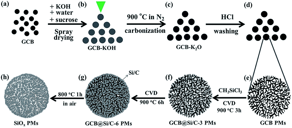 | ||
| Fig. 1 Schematic illustration of the preparation process of GCB PMs, GCB@Si/C-3 PMs, GCB@Si/C-6 PMs, and SiOx PMs. | ||
2.2 Materials characterization
X-ray diffraction (XRD) patterns were recorded on a PANalytical X'Pert PRO MPD using the Cu Kα radiation of (λ = 1.5418 Å). The microscopic feature of the samples was characterized by field-emission scanning electron microscopy (FESEM) with an energy-dispersive X-ray spectrometer (EDX) (JSM-7001F, JEOL, Tokyo, Japan) and transmission electron microscopy (TEM) (JEM-2010F, JEOL, Tokyo, Japan). The porous property of the samples was investigated using physical adsorption of nitrogen at liquid-nitrogen temperature (−196 °C) on an automatic volumetric sorption analyzer (NOVA3200e, Quantachrome). Prior to the measurement, the sample was degassed at 200 °C for 24 h under vacuum. The specific surface area was determined according to the Brunauer–Emmett–Teller (BET) method in the relative pressure range of 0.05–0.2. The particle size distribution (PSD) was measured using a laser particle size analyzer (Model BT-9300Z, Bettersize Instruments, Ltd, China). Thermogravimetric (TG) analysis was carried out on an EXSTAR TG/DTA 6300 (Seiko Instruments, Japan) at a heating rate of 10 °C min−1 in air (200 mL min−1).2.3 Electrochemical measurement
The working electrode was prepared by mixing the active materials, acetylene black, and polyvinylidene fluoride (PVDF) at a weight ratio of 80![[thin space (1/6-em)]](https://www.rsc.org/images/entities/char_2009.gif) :10:10 with N-methylpyrrolidone (NMP) as the solvent. The resulting slurries were cast onto a common Cu foil (current collector). The film composed of Cu foil and slurries were rolled into 25 μm thin sheets, and then dried at 50 °C for 24 h. The film were cut into disks with a diameter of 14 mm, and then dried at 120 °C in vacuum for 24 h. CR2016 coin-type cells were assembled in an Ar-filled glove box with lithium foils as the counter electrodes and polypropylene microporous films (Celgard 2400) as separators. The liquid electrolyte is 1 mol L−1 LiPF6 in a mixture of ethylene carbonate (EC) and dimethyl carbonate (DMC) (1:1, v/v). The galvanostatic charge and discharge tests were carried out on a NEWARE CT-3008-5V10 mA testing instrument in a voltage range between 0.01 and 1.0 V at current densities of 100, 200, 500, and 1000 mA g−1. Electrochemical impedance spectroscopy (EIS) measurements were conducted using a CHI660D potentiostat over a frequency range from 100 kHz to 10 mHz with an ac oscillation of 5 mV. The capacity of all samples is calculated based on the mass of only active materials.
:10:10 with N-methylpyrrolidone (NMP) as the solvent. The resulting slurries were cast onto a common Cu foil (current collector). The film composed of Cu foil and slurries were rolled into 25 μm thin sheets, and then dried at 50 °C for 24 h. The film were cut into disks with a diameter of 14 mm, and then dried at 120 °C in vacuum for 24 h. CR2016 coin-type cells were assembled in an Ar-filled glove box with lithium foils as the counter electrodes and polypropylene microporous films (Celgard 2400) as separators. The liquid electrolyte is 1 mol L−1 LiPF6 in a mixture of ethylene carbonate (EC) and dimethyl carbonate (DMC) (1:1, v/v). The galvanostatic charge and discharge tests were carried out on a NEWARE CT-3008-5V10 mA testing instrument in a voltage range between 0.01 and 1.0 V at current densities of 100, 200, 500, and 1000 mA g−1. Electrochemical impedance spectroscopy (EIS) measurements were conducted using a CHI660D potentiostat over a frequency range from 100 kHz to 10 mHz with an ac oscillation of 5 mV. The capacity of all samples is calculated based on the mass of only active materials.
3. Results and discussion
Fig. 2a indicates the SEM image of graphitized carbon black-containing porous microspheres (GCB PMs) which have diameters between 1 to 5 μm. The enlarged SEM image of GCB PMs (Fig. 2b) shows a good spherical morphology, and the microspheres are composed of GCB nanoparticles (Fig. 2c) with several tenth of nanometers in size, which act as the building block units forming porous structure. The TEM image of Fig. 2d reveals the detailed hollow structure of GCB nanoparticles. The hollow core has a void space of about several nanometers and the shell with a thickness of around several nanometers. The lattice plane distance is measured to be around 0.339 nm (inset of Fig. 2d), suggesting the higher graphitic degree of GCB nanoparticles. | ||
| Fig. 2 SEM images of GCB PMs (a, and b), and the surface of GCB PMs (c), and TEM image of GCB (d) (inset is its high resolution TEM image). | ||
Fig. 3a shows the SEM image of GCB@Si/C-3 PMs with the size range of approximately 1–5 μm. Compared with the GCB PMs (Fig. 2c), the surface of the pore structure becomes smoother because of coating of the amorphous Si/C layers on the GCB nanoparticles (Fig. 3b). These originally separated GCB nanoparticles are connected by amorphous Si/C nanoparticles. The elemental mapping images taken from the SEM image of the Fig. 3c show a uniform elemental distribution of C (Fig. 3d) and Si (Fig. 3e) in the whole GCB@Si/C-3 PMs. EDX spectroscopy (Fig. 3f) shows that this sample is composed of C, Si, and O at a mass ratio of approximately 80:16:4, revealing the C and Si elements are the dominant components.
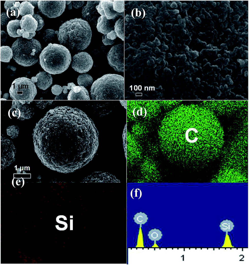 | ||
| Fig. 3 SEM images of GCB@Si/C-3 PMs (a), the surface of GCB@Si/C-3 PMs (b), and several GCB@Si/C-3 PMs (c), elemental mapping images of C (d) and Si (e), and their EDX spectroscopy (f). | ||
Fig. 4a indicates the SEM image of GCB@Si/C-6 PMs with a diameter of 1–5 μm. Differing from GCB PMs (Fig 2c) and GCB@Si/C-3 PMs (Fig. 3b), most of the pores on the surface of GCB PMs have disappeared due to coating of the amorphous Si/C on GCB (Fig. 4b). All the GCB nanoparticles are connected with each other to form dense network structures. The elemental mapping images taken from GCB@Si/C-6 PMs also show a uniform elemental distribution of C and Si in the whole GCB@Si/C-6 PMs (Fig. 4c). EDX spectroscopy (Fig. 4c) shows that this sample is composed of C, Si, and O with a mass ratio of approximately 70:25:5, in which, the Si and C elements are predominant. The TEM image in Fig. 4d reveals the presence of stacked graphene layers roughly parallel to the surface of amorphous Si/C layers, indicating a turbostratic structure. The corresponding selected-area electron diffraction (SAED) pattern (inset of Fig. 4d) shows an amorphous nature of the Si/C layers.
 | ||
| Fig. 4 SEM images of GCB@Si/C-6 PMs (a), the surface of GCB@Si/C-6 PMs (b), several GCB@Si/C-6 PMs, elemental mapping images of C and Si, and their EDX spectroscopy (c), and high resolution TEM image of the amorphous Si/C layers (d) (inset is its SAED pattern). | ||
Fig. 5a and b shows the SEM images of amorphous SiOx PMs, which consists of GCB@Si/C-6 PMs with a diameter of about 1–5 μm. The EDX spectroscopy (inset of Fig. 5a) indicates that this sample is composed of C, Si, and O at an atomic ratio of approximately 4:40:56, of which, the Si and O elements are the dominant components, suggesting that most of the Si reacted with O2 to form SiOx during the calcination process, and most of C was combusted with O2 in air at 800 °C. The TEM images of amorphous SiOx PMs (Fig. 5c and d) show that these microspheres are porous structure after calcination in air, in which, the porous microsphere are composed of hollow SiOx nanoparticles due to removal of GCB nanoparticles (Fig. 5e), suggesting the amorphous Si/C uniformly coated on the surface of GCB nanoparticles.
 | ||
| Fig. 5 SEM images of amorphous SiOx PMs (a, and b) (inset is its EDX spectroscopy), and TEM images of amorphous SiOx PMs (c–e). | ||
Fig. 6a shows the XRD patterns of all the samples. There are several diffraction peaks at 2θ values of 26.8, 43.7, 55.6, and 78.6° for GCB PMs, GCB@Si/C-3 PMs, and GCB@Si/C-6 PMs, which are assigned to (002), (101), (004), and (110) planes of graphite (JCPDS no. 65-6212), suggesting the absence of crystalline Si in these samples.47 For the SiOx PMs sample, the broaden XRD diffraction peak between 20 and 30° indicates the presence of SiOx after calcination at 800 °C in air.44 The PSD curves (not shown here) reveals that the particle sizes of GCB PMs, GCB@Si/C-3 PMs, GCB@Si/C-6 PMs, and SiOx PMs is in the range of about 0.5–15 μm. Fig. 6b shows the TG curves of the GCB PMs, GCB@Si/C-3 PMs, and GCB@Si/C-6 PMs. For the GCB@Si/C-3 PMs, there is a weight loss of about 84.1 wt% between 500 and 830 °C, which is ascribed to the combustion of GCB and amorphous C, suggesting that there is about 15.9 wt% of Si in the GCB@Si/C-3 PMs. For GCB@Si/C-6 PMs, the weight loss is about 69.6 wt% from 500 to 800 °C, also due to the burning of GCB and amorphous C, indicating that about 30.4 wt% of mass is Si in GCB@Si/C-6 PMs. More importantly, almost no residue was observed for the GCB PMs samples, suggesting they have a very high purity, which is required for stability of LIBs materials. The measured N2 adsorption/desorption isotherms (not shown here) reveals that the BET surface areas for GCB PMs, GCB@Si/C-3 PMs, GCB@Si/C-6 PMs, and SiOx PMs are 602.2, 280.8, 42.8, and 122.4 m2 g−1, respectively, suggesting the surface area become smaller with prolonged CVD time by coating more amorphous Si/C on GCB. The above characterizations prove that the prepared GCB@Si/C PMs are composed of C and amorphous Si.
 | ||
| Fig. 6 XRD patterns for GCB PMs, GCB@Si/C-3 PMs, GCB@Si/C-6 PMs, and SiOx PMs (a), and TG curves for GCB PMs, GCB@Si/C-3 PMs, and GCB@Si/C-6 PMs (b). | ||
As shown in Fig. 7a, the discharge and charge capacities in the first run are 789.7 and 361.1 mA h g−1 for GCB PMs, 1014.1 and 678.3 mA h g−1 for GCB@Si/C-3 PMs, 1284.4 and 874.8 mA h g−1 for GCB@Si/C-6 PMs, and 1426.5 and 630.5 mA h g−1 for SiOx PMs, and accordingly their initial coulombic efficiencies are around 42.3, 64.1, 66.2, and 44.2% in the first cycle, respectively. These irreversible capacity losses can be attributed mainly to the formation of solid electrolyte interphase (SEI) on the surface of the electrode, and also to the irreversible insertion of lithium ions into the amorphous Si nanoparticles. Compared with GCB PMs, the higher voltage plateau for SiOx PMs, GCB@Si/C-3 PMs, and GCB@Si/C-6 PMs are observed at about 0.30–0.50 V, which is attributed to the delithiation (Li extraction) of Si. As shown in Fig. 7b, after 200 cycles, the discharge capacity of GCB@Si/C-3 PMs and GCB@Si/C-6 PMs is 587.2 and 729.7 mA h g−1, respectively, which are higher than those of GCB PMs (331.1 mA h g−1) and SiOx PMs (402.2 mA h g−1). It should be mentioned that the capacity of GCB@Si/C-3 PMs and GCB@Si/C-6 PMs is also higher than that of the reported Si/SiOx/C composites (578 mA h g−1 at the 90th cycle)48 and SiO2/C composites (above 500 mA h g−1 at 50th cycle),49 but lower than that of the Si/C composites (1459 mA h g−1 after 200 cycles)50 and Si/C/graphene composites (1521 mA h g−1 after 200 cycles).51 Meanwhile, an average capacity fading rate of GCB PMs, GCB@Si/C-3 PMs, and GCB@Si/C-6 PMs is around 0.04, 0.07, and 0.09% per cycle, respectively, which are lower than those of SiOx PMs (0.18% per cycle). The areal density of GCB PMs, SiOx PMs, GCB@Si/C-3 PMs and GCB@Si/C-6 PMs is calculated to be about 2.60, 1.99, 3.90, and 3.92 mg cm−2. The Si mass loading in the present study is typically 0.62 and 1.18 mg cm−2 for GCB@Si/C-3 PMs and GCB@Si/C-6 PMs, which is higher than that of conducting hydrogel coat Si nanoparticles (0.2–0.3 mg cm−2)52 and Si/PFFOMB electrode (0.2 mg cm−2).53 This maybe because of spherical morphology have high packing density for high volumetric energy and power density, as well as good particle mobility to form a uniformly compact electrode layer. In addition, the areal capacity of GCB@Si/C-3 PMs and GCB@Si/C-6 PMs after 200 cycles is calculated to be 2.29 and 2.85 mA h cm−2, which is higher than that of the GCB PMs (1.29 mA h cm−2) and SiOx PMs (1.57 mA h cm−2) (with respect to the total areal of the electrode including active materials, acetylene black, and PVDF). The rate performance of the GCB@Si/C-3 PMs in Fig. 7c shows that GCB@Si/C-3 PMs delivers a capacity of 637.1, 597.5, 524.6, 362.6, and 620.8 mA h g−1 and the capacity retention is close to 96.5, 96.8, 97.9, 94.5, and 98.4% after 20 cycles at 100, 200, 500, 1000, and 100 mA g−1, respectively. Fig. 7d shows the Nyquist plots of all the samples. It is well known that the impedance plot is consisted of one semicircle curve that corresponds to the resistance of the Li ion transfer through SEI layers in the high frequency range, and a straight line to the resistance for charge transfer at the electrode/electrolyte interface and the Li ion Warburg diffusion resistance in the solid electrode material in the low frequency range. These Nyquist plots show that SiOx PMs have the largest semicircles with the highest charge transfer resistance, suggesting the lowest electronic conductivity. The introduction of GCB with good electronic conductivity within GCB@Si/C-3 PMs, and GCB@Si/C-6 PMs leads to the relatively small semicircles, which promote their electrochemical performance. In addition, GCB PMs shows the smallest semicircles, implying the lowest charge transfer resistance and the highest electronic conductivity. Although the prepared GCB@Si/C PMs show the good electrochemical properties, it is still necessary to further improve their initial coulombic efficiency and cycling properties by controlling the mass ratio of Si and C and the pore structure of porous microspheres. It should be mentioned that the prepared GCB PMs can be used as carbon support,54 water adsorption,55 supercapacitors,56 or electronics,57 and the prepared amorphous SiOx PMs can be used as rubber additive,58 catalyst carrier,59,60 etc.
 | ||
| Fig. 7 Electrochemical properties: the initial discharge–charge (a), and cycling property (b) of all the samples at a current density of 100 mA g−1, the rate performance of GCB@Si/C-3 PMs at different current densities (c), and Nyquist plots of all the samples at the electrode potentials from 0.70 to 0.10 V (d). | ||
4. Conclusions
In summary, we have synthesized novel graphitized carbon black porous microspheres coated with amorphous silicon/carbon layers (GCB@Si/C PMs) by employing techniques of spray drying, KOH activation, and chemical vapor deposition in the preparation. Meanwhile, we have demonstrated GCB@Si/C PMs is a kind of high-performance anode material with long cycle life (200 cycles with 86.6% capacity retention), high specific capacity (about 637.1, 597.5, 524.6, 362.6, and 620.8 mA h g−1 at current density of 100, 200, 500, 1000, and 100 mA g−1). These performance parameters are close to the requirements for the next generation of high-performance batteries for portable electronics, electric vehicles, and grid-scale applications. Furthermore, the use of low-cost GCB and methyltrichlorosilane as the Si and C precursors is expected to significantly lower the production cost of Si/C composite materials, making it feasible for industrial production of the Si/C anode materials and some other applications.Acknowledgements
The authors gratefully acknowledge the supports from the National Natural Science Foundation of China (no. 51402299, 51402302, and 51272252) and Hundred Talents Program of the Chinese Academy of Sciences.Notes and references
- M. Armand and J. M. Tarascon, Nature, 2008, 451, 652 CrossRef CAS PubMed.
- B. Scrosati, J. Hassoun and Y. K. Sun, Energy Environ. Sci., 2011, 4, 3287 CAS.
- B. L. Ellis, K. Town and L. F. Nazar, Electrochim. Acta, 2012, 84, 145 CrossRef CAS.
- Z. Zhang, Y. Wang, W. Ren, Q. Tan, Y. Chen, H. Li, Z. Zhong and F. Su, Angew. Chem., Int. Ed., 2014, 53, 5165 CAS.
- J. Cho, J. Mater. Chem., 2010, 20, 4009 RSC.
- I. Kovalenko, B. Zdyrko, A. Magasinski, B. Hertzberg, Z. Milicev, R. Burtovyy, I. Luzinov and G. Yushin, Science, 2011, 334, 75 CrossRef CAS PubMed.
- M. Gu, X. C. Xiao, G. Liu, S. Thevuthasan, D. R. Baer, J. G. Zhang, J. Liu, N. D. Browning and C. M. Wang, Sci. Rep., 2014, 4, 3684 Search PubMed.
- C. Martin, Nat. Nanotechnol., 2014, 9, 327 CrossRef CAS PubMed.
- H. Wu and Y. Cui, Nano Today, 2012, 7, 414 CrossRef CAS.
- C. Wang, H. Wu, Z. Chen, M. T. McDowell, Y. Cui and Z. Bao, Nat. Chem., 2013, 5, 1042 CrossRef CAS PubMed.
- M. T. McDowell, S. W. Lee, W. D. Nix and Y. Cui, Adv. Mater., 2013, 25, 4966 CrossRef CAS PubMed.
- J. Wan, A. F. Kaplan, J. Zheng, X. Han, Y. Chen, N. J. Weadock, N. Faenza, S. Lacey, T. Li, J. Guo and L. Hu, J. Mater. Chem. A, 2014, 2, 6051 CAS.
- V. Chakrapani, F. Rusli, M. A. Filler and P. A. Kohl, J. Power Sources, 2012, 205, 433 CrossRef CAS.
- J. H. Cho and S. T. Picraux, Nano Lett., 2013, 13, 5740 CrossRef CAS PubMed.
- Z. Wen, G. Lu, S. Mao, H. Kim, S. Cui, K. Yu, X. Huang, P. T. Hurley, O. Mao and J. Chen, Electrochem. Commun., 2013, 29, 67 CrossRef CAS.
- H. Wu, G. Chan, J. W. Choi, Y. Yao, M. T. McDowell, S. W. Lee, A. Jackson, Y. Yang, L. Hu and Y. Cui, Nat. Nanotechnol., 2012, 7, 310 CrossRef CAS PubMed.
- J. K. Yoo, J. Kim, Y. S. Jung and K. Kang, Adv. Mater., 2012, 24, 5452 CrossRef CAS PubMed.
- Y. Yao, M. T. McDowell, I. Ryu, H. Wu, N. Liu, L. Hu, W. D. Nix and Y. Cui, Nano Lett., 2011, 11, 2949 CrossRef CAS PubMed.
- E. Hüger, L. Dörrer, J. Rahn, T. Panzner, J. Stahn, G. Lilienkamp and H. Schmidt, Nano Lett., 2013, 13, 1237 CrossRef PubMed.
- J. R. Szczech and S. Jin, Energy Environ. Sci., 2011, 4, 56 CAS.
- M. L. Terranova, S. Orlanducci, E. Tamburri, V. Guglielmotti and M. Rossi, J. Power Sources, 2014, 246, 167 CrossRef CAS.
- K. Shin, D. J. Park, H. S. Lim, Y. K. Sun and K. D. Suh, Electrochim. Acta, 2011, 58, 578 CrossRef CAS.
- L. Hu, N. Liu, M. Eskilsson, G. Zheng, J. McDonough, L. Wågberg and Y. Cui, Nano Energy, 2013, 2, 138 CrossRef CAS.
- X. Zhu, H. Chen, Y. Wang, L. Xia, Q. Tan, H. Li, Z. Zhong, F. Su and X. S. Zhao, J. Mater. Chem., 2013, 1, 4483 RSC.
- X. Shen, D. Mu, S. Chen, B. Xu, B. Wu and F. Wu, J. Alloys Compd., 2013, 552, 60 CrossRef CAS.
- J. Y. Eom and H. S. Kwon, ACS Appl. Mater. Interfaces, 2011, 3, 1015 CAS.
- J. Park, G. P. Kim, I. Nam, S. Park and J. Yi, Nanotechnology, 2013, 24, 025602 CrossRef PubMed.
- J. Guo, Z. Yang and L. A. Archer, J. Mater. Chem. A, 2013, 1, 5709 CAS.
- M. Zhang, X. Hou, J. Wang, M. Li, S. Hu, Z. Shao and X. Liu, J. Alloys Compd., 2014, 588, 206 CrossRef CAS.
- L. Yue, S. Wang, X. Zhao and L. Zhang, J. Mater. Chem., 2012, 22, 1094 RSC.
- Z. Zhang, Y. Wang, Q. Tan, D. Li, Y. Chen, Z. Zhong and F. Su, Nanoscale, 2014, 6, 371 RSC.
- Y. Yong and L. Z. Fan, Ionics, 2013, 19, 1545 CrossRef CAS.
- X. Zhou, A. M. Cao, L. J. Wan and Y. G. Guo, Nano Res., 2012, 5, 845 CrossRef CAS.
- H. Lin, W. Weng, J. Ren, L. Qiu, Z. Zhang, P. Chen, X. Chen, J. Deng, Y. Wang and H. Peng, Adv. Mater., 2014, 26, 1217 CrossRef CAS PubMed.
- J. K. Yoo, J. Kim, H. Lee, J. Choi, M. J. Choi, D. M. Sim, Y. S. Jung and K. Kang, Nanotechnology, 2013, 24, 424008 CrossRef PubMed.
- N. Liu, Z. Lu, J. Zhao, M. T. McDowell, H.-W. Lee, W. Zhao and Y. Cui, Nat. Nanotechnol., 2014, 9, 187 CrossRef CAS PubMed.
- X. H. Hou, J. Y. Wang, M. Zhang, X. Liu, Z. P. Shao, W. S. Li and S. J. Hu, RSC Adv., 2014, 4, 34615 RSC.
- A. Magasinski, P. Dixon, B. Hertzberg, A. Kvit, J. Ayala and G. Yushin, Nat. Mater., 2010, 9, 461 CrossRef CAS.
- J. H. Lee, W. J. Kim, J. Y. Kim, S. H. Lim and S. M. Lee, J. Power Sources, 2008, 176, 353 CrossRef CAS.
- M. T. McDowell, S. W. Lee, J. T. Harris, B. A. Korgel, C. Wang, W. D. Nix and Y. Cui, Nano Lett., 2013, 13, 758 CrossRef CAS PubMed.
- J. W. Wang, Y. He, F. Fan, X. H. Liu, S. Xia, Y. Liu, C. T. Harris, H. Li, J. Y. Huang, S. X. Mao and T. Zhu, Nano Lett., 2013, 13, 709 CrossRef CAS PubMed.
- C. F. Sun, K. Karki, Z. Jia, H. Liao, Y. Zhang, T. Li, Y. Qi, J. Cumings, G. W. Rubloff and Y. Wang, ACS Nano, 2013, 7, 2717 CrossRef CAS PubMed.
- J. W. Wang, X. H. Liu, K. Zhao, A. Palmer, E. Patten, D. Burton, S. X. Mao, Z. Suo and J. Y. Huang, ACS Nano, 2012, 6, 9158 CrossRef CAS PubMed.
- Z. Zhang, M. Zhang, Y. Wang, Q. Tan, X. Lv, Z. Zhong, H. Li and F. Su, Nanoscale, 2013, 5, 5384 RSC.
- Y. Tong, Z. Xu, C. Liu, G. a. Zhang, J. Wang and Z. G. Wu, J. Power Sources, 2014, 247, 78 CrossRef CAS.
- P. C. Chen, J. Xu, H. Chen and C. Zhou, Nano Res., 2010, 4, 290 CrossRef.
- Y. Wang, F. Su, C. Wood, J. Lee and X. Zhao, Ind. Eng. Chem. Res., 2008, 47, 2294 CrossRef CAS.
- I. Choi, M. J. Lee, S. M. Oh and J. J. Kim, Electrochim. Acta, 2012, 85, 369 CrossRef CAS.
- Y. Yao, J. Zhang, L. Xue, T. Huang and A. Yu, J. Power Sources, 2011, 196, 10240 CrossRef CAS.
- N. Liu, K. Huo, M. T. McDowell, J. Zhao and Y. Cui, Sci. Rep., 2013, 3, 1919 Search PubMed.
- X. Zhou, Y. X. Yin, A. M. Cao, L. J. Wan and Y. G. Guo, ACS Appl. Mater. Interfaces, 2012, 4, 2824 CAS.
- H. Wu, G. H. Yu, L. J. Pan, N. A. Liu, M. T. McDowell, Z. A. Bao and Y. Cui, Nat. Commun., 2013, 4, 1943 Search PubMed.
- G. Liu, S. D. Xun, N. Vukmirovic, X. Y. Song, P. Olalde-Velasco, H. H. Zheng, V. S. Battaglia, L. W. Wang and W. L. Yang, Adv. Mater., 2011, 23, 4679 CrossRef CAS PubMed.
- X. L. Sui, Z. B. Wang, M. Yang, L. Huo, D. M. Gu and G. P. Yin, J. Power Sources, 2014, 255, 43 CrossRef CAS.
- V. T. Nguyen, D. D. Do and D. Nicholson, Carbon, 2014, 66, 629 CrossRef CAS.
- C. W. Wang, Y. Wang, J. Graser, R. Zhao, F. Gao and M. J. O'Connell, ACS Nano, 2013, 7, 11156 CrossRef CAS PubMed.
- K. U. Lee, K. J. Park, O. J. Kwon and J. J. Kim, Curr. Appl. Phys., 2013, 13, 419 CrossRef.
- B. Seo, J. Kang, S. Jang, Y. Kang and W. Kim, J. Nanosci. Nanotechnol., 2013, 13, 2179 CrossRef CAS PubMed.
- P. M. Mortensen, J. D. Grunwaldt, P. A. Jensen and A. D. Jensen, ACS Catal., 2013, 3, 1774 CrossRef CAS.
- G. Prieto, J. D. Meeldijk, K. P. de Jong and P. E. de Jongh, J. Catal., 2013, 303, 31 CrossRef CAS.
| This journal is © The Royal Society of Chemistry 2014 |