Yueyong Yang,
Junyan Xiao,
Huiyun Wei,
Lifeng Zhu,
Dongmei Li,
Yanhong Luo,
Huijue Wu and
Qingbo Meng*
Key Laboratory for Renewable Energy, Chinese Academy of Sciences, Beijing Key Laboratory for New Energy Materials and Devices, Institute of Physics, Chinese Academy of Sciences, Beijing, 100190, People's Republic of China. E-mail: qbmeng@iphy.ac.cn
First published on 16th October 2014
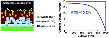
An all-carbon counter electrode has been fabricated for hole-conductor-free organo-metal perovskite heterojunction thin-film solar cells by a simple and low-temperature process. The counter electrode consisted of two parts: a mesoscopic carbon layer for good contact with the perovskite layer, and a piece of industrial flexible graphite sheet as the conducting electrode. Several types of carbon materials were employed in the counter electrodes and tested. From an electrochemical impedance study, it is found that the contact between the counter electrode and perovskite layer has a significant influence on the charge transport properties of the cells. A power conversion efficiency up to 10.2% has been achieved by hole-conductor-free mesoscopic CH3NH3PbI3/TiO2 heterojunction solar cells with the counter electrode containing a composition of graphite and carbon black, which inspires a new promising route towards low-cost and large-scale commercialization of perovskite solar cells.
Counter electrode (CE) plays a very important part in solar cells.11–13 For most organo-metal perovskite solar cells reported so far, Au is the most efficient and widely used CE material. However, Au is expensive and increases the overall manufacturing cost of the perovskite solar cells. Cheaper metals like Ag work well in perovskite cells with HTM layer, but they cannot stay stable in HTM-free perovskite cells.14 Considering the fierce competition of the global photovoltaic market, to make this type of solar cells competitive commercial products, inexpensive CEs with acceptable performance need to be developed.
Carbon materials are low-cost and highly available industrial materials, which have been applied in highly efficient CEs of dye-sensitized solar cells15–18 and quantum dot-sensitized solar cells.19 The approximate 5.0 eV work function makes carbon the ideal CE material for perovskite solar cells.20 Recently, several types of carbon CEs have been applied successfully in perovskite solar cells,20–22 suggesting that carbon materials are prospective candidates of CE materials for hole-conductor-free perovskite solar cells. However, some issues of the carbon CE still exist: (1) currently most fabrication methods were relatively complicated, which induced additional high-temperature procedures or redeveloped optimized methods for photoelectrodes, and (2) the key factors influencing the performance of CEs was not clear enough. Therefore, it is of significant importance to develop new carbon CEs for perovskite solar cells and further study its mechanism.
Here, we report a simple and low-temperature processable all-carbon flexible CE for highly efficient perovskite solar cells. Industrial flexible graphite sheet was used as the conducting electrode and a mesoscopic carbon layer was used for the good contact with the perovskite layer. A two-step process was employed to fabricate the CEs. In this process, no insulating space layer or additional high-temperature sintering procedure were needed. This carbon CE can adapt to any hole-conductor-free perovskite solar cells without changing the current process of fabricating photoelectrodes. By the optimization of CE components, a PCE of 10.2% has been achieved by hole-conductor-free mesoscopic CH3NH3PbI3/TiO2 heterojunction solar cells. Moreover, the key factors influencing the performance of carbon CEs have been investigated, which can help exploit the potential improvement of perovskite solar cells with carbon CEs in the future.
![]() | ||
Fig. 1 Scheme of the fabrication process of all-carbon flexible CE based HTM-free perovskite solar cells. |
The surface morphology of CE A, B, C and D are shown in Fig. 2. The accumulation structure of graphite flakes can be clearly seen in the SEM images. Estimated from the SEM images, the sizes of graphite flakes in CE A, B and C are around 20 μm, 3 μm and 1 μm, respectively. In CE D, a composite structure of graphite and CB can be observed. The size of CB particles is less than 100 nm. The small CB particles fill in the interspace between the graphite flakes, and are held tightly on the graphite framework by the binder. The SEM cross-section image of the HTM-free perovskite solar cell with CE D is shown in Fig. 2(g) and (h). The thickness of the FTO layer, mesoscopic TiO2 layer, perovskite capping layer and mesoscopic carbon layer is 359 nm, 449 nm, 359 nm and 23 μm, respectively.
The conductivity of the mesoscopic carbon films was measured. These films were first coated on insulated glass substrate by screen-printing technique. A four-point probe resistivity measurement system was employed to measure the sheet resistance of the carbon films. The thickness of the carbon films was measured by a profiler. The final results of resistivity are shown in Table 1. The resistivity of CE sample A, B, C and D is 0.127, 0.677, 0.941 and 0.802 Ω cm, respectively. CEs that contain larger graphite flakes exhibit better conductivity. The differences in the conductivity of the CE A, B and C are probably caused by the different densities of interfaces between carbon flakes. For CEs with smaller graphite flakes, there are more interfaces between different graphite flakes, which contributes higher contact resistance to the mesoscopic carbon film. On the other hand, the graphite/CB composite CE (CE D) shows quite closed resistivity compared with CE C, suggesting that in graphite/CB composite CE, the graphite framework is still the major pathway of charge transportation in the composite carbon film. Although the small CB particles create more interfaces, they do not influence much on the overall conductivity of the CE. In our CE, the thickness of the mesoscopic carbon films was approximately 20 μm. As the flexible graphite sheet, whose sheet resistance is only 4.2 × 10⁻² Ω □−1, is used as the conducting electrode, the total contribution of the carbon CE to the series resistance of the cell is quite small.
CE sample | Graphite flake size | Graphite wt% | CB wt% | Resistivity (Ω cm) |
---|---|---|---|---|
A | 20 μm | 95% | 0 | 0.127 |
B | 3 μm | 95% | 0 | 0.677 |
C | 1 μm | 95% | 0 | 0.941 |
D | 1 μm | 75% | 20% | 0.802 |
The J–V characteristics of HTM-free CH3NH3PbI3/TiO2 heterojunction solar cells with different CEs were evaluated. The J–V curves of the representatives of these cells tested under AM 1.5 100 mW cm−2 are shown in Fig. 3(b). Detailed data are presented in Table 2. Fig. 3(c)–(f) are the box charts exhibiting the statistical features of short-circuit current density (JSC), open-circuit voltage (VOC), fill factor (FF) and PCE of all the cells with carbon CEs tested. Cells with CE A, which contain the largest graphite flakes, show the poorest performance. The fill factor is as low as 0.301, and the JSC value is obviously lower than other cells. Cells with CE B, C and D exhibit similar JSC values of more than 18 mA cm−2. Improved performances are achieved by cells with CE B and CE C, of which the fill factor rise to over 0.4, revealing the improvement by the change of graphite flake sizes. The cells with CE D achieve the highest efficiency up to 10.2%, which is only a little lower than the 10.73% efficiency of cells with the expensive Au CE, and the fill factor reaches 0.572. These results show that CEs containing smaller graphite flakes exhibit much better photovoltaic performance compared with CEs consisting of bigger graphite flakes. Moreover, the adding of small CB particles in the CE can further improve the cell performance, especially fill factor. Meanwhile, the over 10% efficiency of HTM-free perovskite cells also clearly demonstrates that our flexible carbon CE is comparable with the expensive Au CE, considering our current technique level of fabricating HTM-free perovskite photoelectrodes.8 Once better photoelectrodes were used, this type of carbon CE could probably achieve even higher efficiency.
CE sample | JSC (mA cm−2) | VOC (mV) | Fill factor | PCE (%) |
---|---|---|---|---|
A | 15.29 | 816.3 | 0.301 | 3.76 |
B | 18.30 | 837.2 | 0.402 | 6.16 |
C | 18.85 | 921.2 | 0.415 | 7.21 |
D | 18.73 | 952.7 | 0.572 | 10.20 |
Au | 18.15 | 910.7 | 0.649 | 10.73 |
The electrochemical impedance spectroscopy (EIS) of the cells with both Au CE and our carbon CEs were measured under dark condition at different forward applied bias to investigate the charge transport properties. The Nyquist plots of cells with CE D are presented in Fig. 4(b) as an example. The arc in the Nyquist plots becomes smaller as the applied bias increases. This arc could be related to the overall charge transport in the cell, including the contribution of TiO2/perovskite interface, perovskite layer and perovskite/CE interface (the perovskite layer and perovskite/CE interface are denoted as “back contact”).23–25 The simplified model in Fig. 4(a) was used to fit the measured results.26 The fitted values of RCT for cells with different CEs are shown in Fig. 4(c). Significant differences exists between these cells. Cells with Au CE exhibit the lowest RCT level. For cells with carbon CEs, RCT level increases in order of CE D, C, B and A. This result is quite interesting because the charge transfer resistance at the TiO2/perovskite interface in these cells should be close to each other, as the photoelectrodes of the cells were fabricated under the same process. Considering that the CE is the only different part in these cells, it can be concluded that the RCT level in perovskite layer is influenced by different CEs. In EIS measurement under dark conditions, the impedances related to TiO2/perovskite interface and the back contact are series connected. The influence of the back contact can be directly reflected on the measured RCT values. For cells with better back contact, the contribution of the perovskite layer and perovskite/CE interface is smaller, and thus exhibiting smaller RCT values.
The differences in charge transfer resistance contributed by back contact are probably due to the different contact between the perovskite layer and CE. For cells with evaporated Au CE, typically the CE can have quite good contact with the CH3NH3PbI3 layer. In this case, charges tend to travel the shortest distance through the CH3NH3PbI3 layer, and thus exhibit the lowest charge transport resistance. However, for cells with carbon CE, the situation is quite different. Because of the undulation at the surface of graphite flakes, the graphite flakes and CH3NH3PbI3 layer cannot fully contact. The limited contact sites forces the charges to transport through longer distance in the perovskite layer (Fig. 5(a)), which increases the charge transport resistance. By comparing the RCT levels of cells with CE A, B and C, it can be deduced that the bigger size the graphite flakes have, the fewer contact sites at CH3NH3PbI3/CE interface. As for the graphite/CB composite CE (CE D), the lowest RCT level in cells with carbon CEs suggests that the gentler undulation at the surface of smaller graphite flakes, together with the CB particles in the interspace create the most contact sites with the perovskite layer among all the carbon CEs (Fig. 5(b)).
![]() | ||
Fig. 5 Scheme of charge transfer in HTM-free CH3NH3PbI3/TiO2 heterojunction solar cells with CE consisting of (a) large graphite flakes; (b) composition of smaller graphite flakes and CB particles. |
The contact between the CE and perovskite layer affects the cell performance not only by influencing the charge transport resistance in perovskite layer, but may also by possibly altering the charge transfer process at the CH3NH3PbI3/CE interface. In dye-sensitized solar cells27,28 and quantum-dot sensitized solar cells,29,30 the surface area of CE is one of the key factors influencing the cell performance.16,31–33 CEs with higher surface area have more catalytic sites contacting the electrolyte, and thus exhibit better charge transfer property. In HTM-free perovskite solar cells, holes are transported to the CH3NH3PbI3/CE interface, where charge transfer occurs to finish the working cycle of the cell. Similarly, the good contact between the CE and CH3NH3PbI3 layer is crucial for the smooth charge transfer process. As the differences of contact sites between different CEs are fierce, it is reasonable to suppose that the charge transfer ability at the CH3NH3PbI3/CE interface is affected significantly. For cells with unsatisfactory CH3NH3PbI3/CE contact, there may be a bottleneck for the charge transfer process. In this work, the use of smaller graphite flakes and carbon black particles can improve the charge transfer by increasing the contact sites in some degree, which remarkably improve the performance of the cells. Further optimization of the contact between CH3NH3PbI3 layer and carbon CE by interface engineering may achieve an even higher efficiency in the future.
Substrates for photoelectrode are fluorine-doped tin oxide conducting glass (FTO, Pilkington, thickness: 2.2 mm, sheet resistance 14 Ω square−1). Before use, FTO glass was firstly washed with mild detergent, rinsed with distilled water for several times and subsequently with ethanol in an ultrasonic bath, finally dried under air stream. The flexible graphite sheets with thickness of 0.2 mm and area density of 0.03 g cm−2 were cleaned with distilled water, ethanol and then air-dried.
Footnote |
† Electronic supplementary information (ESI) available: It includes the photovoltaic properties of perovskite solar cells with different graphite/CB ratio, and fitted RS values in EIS results. See DOI: 10.1039/c4ra09519g |
This journal is © The Royal Society of Chemistry 2014 |