Alcohol mediated growth of α-MnO2 thin films from KMnO4 precursor for high performance supercapacitors

Nilesh R. Chodankara, Girish S. Gunda, Deepak P. Dubalb and Chandrakant D. Lokhande*a
aThin Film Physics Laboratory, Department of Physics, Shivaji University, Kolhapur-416004, MS, India. E-mail: l_chandrakant@yahoo.com; Fax: +91 231 2609233; Tel: +91 231 2609225
bCatalan Institute of Nanoscience and Nanotechnology, CIN2, ICN2 (CSIC-ICN), Campus UAB, E-08193 Bellaterra, Barcelona, Spain

Received 26th August 2014 , Accepted 3rd November 2014

First published on 4th November 2014


Abstract

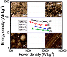
Energy storage devices, with low cost, high energy density, high power density, and long cycle life, have prime importance in order to solve the problem of interrupted power supply of renewable generation systems. In the present work, MnO2 thin films have been deposited by a simple, scalable, additive-free, binder-less, low cost, low temperature and eco-friendly chemical bath deposition method. The impact of three different alcohols (methanol, ethanol, 2-propenol) as reducing agents on the morphological, structural and electrochemical properties of MnO2 thin film is investigated. The MnO2 thin film prepared with the methanol as the reducing agent exhibits high specific surface area with excellent electrochemical features such as high specific capacitance of 633 F g−1 and high energy density of 65.9 W h kg−1 at current density of 1 mA cm−2 along with a good cycling stability of 95% after 2000 CV cycles. Such leading electrochemical properties suggest that MnO2 thin film prepared with methanol as the reducing agent using chemical bath deposition is a significant method to prepare reliable electrode material for future energy storage devices.


1. Introduction

The limited availability of fossil fuel has actuated enormous research efforts for developing renewable energy conversion technologies and energy storage systems to solve the problem of the interrupted power supply of renewable energy resources. In the future, people will be entirely reliant on non-conventional energy sources to accomplish their energy requirements, and these sources are not present all the time, so the use of energy storage devices is essential.1 Supercapacitors (SCs) represent one of the most attractive classes of energy storage device that exhibits fast charge–discharge rate, high power density, with long cycle lifetime and have a number of applications from portable electronic devices to hybrid electronic vehicles.2–4 The energy storing capacity of SCs is small as compared to batteries, so most of the efforts focused on improving the energy density of SCs without diminishing their power density and cycling stability.5 SCs are classified on the basis of charge storage mechanism: (i) electrical double layer capacitors (EDLCs). EDLCs (usually exhibited by carbon material) store electrical charges at the interface of electrode–electrolyte. The charge storing capacity of EDLCs strongly depends upon pore size distribution and surface area of active electrode material. (ii) Pseudocapacitors store energy through fast and reversible redox (faradic) reaction at the surface as well as in the bulk of active electrode material. The transition metal oxide and conducing polymer exhibit pseudocapacitive behavior.6,7 (iii) The hybrid capacitor is a combination of two charge storage mechanisms i.e. EDLCs and pseudocapacitor, meaning there is a fusing of faradic and non-Faradic reactions.

To commercialize the SCs technology for large-scale application, the electrodes must be inexpensive, scalable, and have low cost processing, having high energy and power densities with high rate capability. From these points of view, metal oxides are excellent electrode materials.8 Among different transition metal oxides, ruthenium oxide (RuO2) has been widely studied due to its high electrical conductivity and different oxidation states with the large potential window of 1.2 V, but its high cost and toxic nature restricts its commercialization.9,10 The oxides of nickel11 cobalt12 and copper13 have been studied but none of these have been investigated as much as manganese oxide.14–16 Among different polymorphs of manganese oxide (MnO, Mn3O4, Mn2O3, MnO2), MnO2 is the most studied material due to its high theoretical specific capacitance (1370 F g−1), low cost (12th most abundant element on the earth), environmental benignity, and excellent electrochemical performance.17–20 MnO2 has been prepared in two different ways as powder and thin film forms. MnO2 powder was prepared by hydrothermal,21 sonochemical22 and precipitation23 methods. The powders were pasted on the current collector with the appropriate amount of additive and binder, which enhance the dead surface area and the mass of the electrode as a result of an increment in contact resistance and decrement in power capability.1 Subramanian et al.24 prepared MnO2 powder by precipitation method using KMnO4 and different alcohols; they obtained maximum specific capacitance of 202 F g−1. MnO2 in thin film form reduces the contact resistance, leading to enhanced electrochemical performance. Presently, MnO2 thin films are prepared through sol–gel,25 electrodeposition26 and chemical bath deposition (CBD)27 methods. Dubal et al.28 prepared α-MnO2 through the CBD method and obtained specific capacitance of 328 F g−1. Among these, CBD is less investigated in terms of dealing with MnO2. The CBD is a soft chemical method, suitable for large scale production, and is low cost and environmentally friendly. The low reaction temperature makes this method more appealing and the features of materials such as structure, morphology, dimensions and phase can be easily controlled through adjusting the preparative parameters such as the reaction time, reaction temperature, concentration of matrix solution, complexing agent, reducing agent, etc.

To solve the above critical problems, we demonstrate a novel reducing agent-assisted chemical bath deposition method for the preparation of MnO2 thin films. The effect of different reducing agents on the structure and morphology is studied. The reducing agent-assisted chemical bath deposition method is very efficient in order to alter microstructure and, subsequently, the effect of microstructure variation on electrochemical properties is analyzed. Moreover, all electrochemical measurements are carried out within a large potential window of 1 V per SCE (between 0 to +1 V per SCE) in Na2SO4 electrolyte.

2. Experimental

Chemicals

Analytical grade potassium permanganate (KMnO4), methanol, ethanol and 2-propenol were used without further purification. Stainless steel (SS) substrates were mirror polished with emery polish paper, cleaned with double distilled water (DDW) and dried at room temperature.

Synthesis of MnO2 thin films

In the present work, MnO2 thin films were deposited using the CBD method. For preparation of MnO2 thin films, the starting material was KMnO4, while methanol, ethanol and 2-propenol were used as the reducing agents. The matrix solutions were prepared by dissolving 0.05 M KMnO4 in 50 mL of DDW in four different beakers. The prepared solutions were stirred for 10 min at room temperature to ensure homogenous distribution of the KMnO4 reagent. Furthermore, 2 mL of methanol, ethanol and 2-propenol were added in the first beakers, separately, while the fourth beaker contained bare KMnO4 solution. The well-cleaned SS substrates were vertically immersed in the above prepared solutions. The reducing agent assisted baths were kept at room temperature for 12 h, while the bare solution bath was kept at 70 °C for 7 h. After deposition, the substrates were taken out from the bath, washed several times in DDW and dried at room temperature. The blackish colored MnO2 thin films were deposited on the surface of the SS substrate. The films prepared with methanol, ethanol and 2-propenol as the reducing agents were denoted by M:MnO2, E:MnO2 and P:MnO2, respectively, whereas the bare MnO2 thin film is denoted by B:MnO2.

Materials characterization

The MnO2 thin films were characterized by X-ray diffraction (XRD) analysis for structural study using a Bruker AXS D8 Advance Model with copper radiation (Kα of λ = 1.54 Å). The surface morphology of the prepared thin films was investigated though field-emission scanning electron microscopy (FE-SEM, JEOL JSM 6390). Raman spectra were measured, using a Jobin Yvon Horibra LABRAM-HR visible spectrometer with an argon-ion continuous-wave laser (488 nm) as the excitation source, to confirm the phase of MnO2. The electrochemical measurements were carried out using an Automatic Battery Cycler (WBCS3000) with a three electrode system containing MnO2 thin film as a working electrode, platinum as a counter electrode and saturated calomel electrode (SCE) as a reference electrode in 1 M Na2SO4 solution as an electrolyte.

3. Results and discussion

Film formation and reaction mechanism

In the CBD method, there are two types of growth mechanisms during the thin film formation: (i) ion-by-ions growth, where the ions are deposited sequentially at the nucleation sites on the surface of the substrate and (ii) adsorption of colloidal particles to form nuclei and then these particles grow by aggregation and coalescence to form a thin film, which is known as cluster-by-cluster growth mechanism.29

For deposition of the MnO2 thin films, KMnO4 was used as a precursor solution. For the morphology evolution, three reducing agents were used, i.e. methanol, ethanol and 2-propenol. In the initial stage, 0.05 M KMnO4 was added in three different beakers to form an intense pinkish precipitate free solution. Furthermore, 2 mL of methanol, ethanol and 2-propenol were added in the KMnO4 solutions, separately. The well cleaned SS substrates were immersed in the prepared solution baths. The precipitation was started in solution after 4 h. During the precipitation, the solution becomes saturated and the ionic product exceeds the solubility product. The heterogeneous chemical reaction occurred on the SS substrate to form an MnO2 thin film. After 12 h, well adherent blackish MnO2 thin films were developed on the SS substrate. The possible chemical reaction during the film formation was as follows:

 
2KMnO4 + R − OH → 2MnO2 + R − OK + KOH + 3O (1)
where R = CH3, C2H5, C3H7.

At the initial stage of the reaction, the manganese oxide nuclei were developed on the surface of the SS substrate as well as in the solution. Furthermore, these nucleation centers act as basic building blocks to develop the nanostructured thin film. As the ionic product successively exceeds the solubility product, large number of ion are collected around the nucleation centers to form clusters of different sized nanoparticles. Subsequently, the coalescence and growth of these particles lead to thin film formation (Scheme 1).29–31


image file: c4ra09268f-s1.tif
Scheme 1 Schematic representation of the formation of nanostructured MnO2 thin film directly onto the stainless steel substrate for (a) B:MnO2, (b) M:MnO2, (c) E:MnO2 and (d) P:MnO2 through the reducing agent assisted chemical bath deposition method.

The preparation of B:MnO2 thin film was carried out using the 0.05 M KMnO4 solution in 50 mL of DDW. The prepared bath with SS substrate was kept at room temperature for 36 h. Even after completing 36 h, no film formation was observed. This may be due to the unavailability of hydrogen (H+) ions for reduction of Mn(VII) species from KMnO4 solution to Mn(IV) species. In order to study the effect of temperature, the same bath was set at 70 °C and after 7 h well adherent thin film formation takes place. In this process, formation of MnO2 takes place by decomposition of KMnO4 in hot water.32 When the bath achieves the desired temperature, water molecules provide hydrogen (H+) ions for reduction of MnO4 species to MnO2; this can be expressed as:

 
4MnO 4 + 2H2O → 4MnO2 + 4OH + 3O2 (2)

Surface morphological studies

The surface morphologies of CBD prepared MnO2 thin films on SS substrate at three different magnifications are shown in Fig. 1. The SEM study is used to visualize the change in microstructure of B:MnO2, M:MnO2, E:MnO2 and P:MnO2 thin films as a consequence of different reducing agents. As the surface morphology of thin film plays a major role in electrochemical performance by means of intercalation/deintercalation of the electrolyte ions into electrode material, the effective way to improve intercalation rate and cycling stability is to develop superior nanostructured thin films. The B:MnO2 thin film demonstrates the compact, dense surface morphology as depicted in Fig. 1(a–c). Such a compact and densely packed surface morphology reduces the electrochemical active sites and causes an increase in the diffusion resistance of electrode. Due to this, the rate of intercalation and deintercalation of electrolyte ions may be reduced for B:MnO2 thin film. The surface morphology of the M:MnO2 thin film exhibits the formation of three-dimensional (3-D) porous self-assembled spherical interlocked fine nanoparticles with an approximate size of 10–30 nm, (see Fig. 1(d–f)). These nanoparticles are randomly oriented having regular shape and size. The space between the interlocked nanoparticles facilitates the diffusion of electrolyte ions and reduces the diffusion resistance of the electrode. Such a nanostructured porous surface morphology may provide large electrochemical active surface and enhances the rate of electrochemical reactions, which is a favorable feature for SCs application. The surface morphology of E:MnO2 thin film shows the formation of nanoparticles having size in the range of 100–150 nm and these particles are composed of very thin (10 nm) nanoflakes, as illustrated in Fig. 1(g–i). Such nanoflakes composed large nanoparticle-like surface morphology may reduce the electroactive surface area and the porosity of the E:MnO2 thin film, as compared to the M:MnO2 thin film. Due to this, the rate of intercalation/deintercalation of electrolyte ions in the electrode diminishes. The surface morphology of P:MnO2 thin film shown in Fig. 1(j–l) displays macro sized ball compact surface morphology having size in the range of 400–900 nm and these balls are composed of very fine nanoparticles having size 10–30 nm. These micro sized balls reduce the porosity of the thin film as compared to the M:MnO2 and E:MnO2 thin films. This leads to slenderized electrochemical active sites and leads to the diminished electrochemical performance of the P:MnO2 thin film. Such a variation in the microstructures is attributed to the surface maneuvering property of the reducing agent and this influences the kinetics of the reactions. The formation of nanostructured MnO2 is followed by steps of nucleation, aggregation and coalescence of particles to form the thin film. The different reducing agents may offer different degrees of rate for chemical reactions, which leads to the formation of different nanostructures. The possible mechanism for the shape evolution process is elaborated as follows: the initially generated nucleation centers attract more ions from the solution in order to form the nanoparticles. These nanoparticles act as a basic building block to form compact and dense surface morphology. Further, the alcohol assisted growth alters the surface morphology from compact dense to nanoparticles to macro-sized ball like surface morphology, with the same nanoparticles as a basic building block. The change in surface morphology of MnO2 thin films occurs due to the addition of different alcohol, which offers different degree of rate for chemical reaction. The growth rate of M:MnO2 is slow and results in the formation of a highly porous fine nanoparticles composed surface morphology. While the reaction rate, and subsequently growth rate, in E:MnO2 and P:MnO2 is higher, therefore there is formation of surface morphology with dense nanoparticles and micro sized ball like surface morphology having less porosity. Hence, the change in nanostructure brings about fruitful and effective change in the electrochemical properties of the thin films. For M:MnO2 thin film, the porous 3D nanostructure surface morphology provides more electroactive sites of the electrode for electrochemical reaction as compared to E:MnO2 (particles with very thin nanoflakes), P:MnO2 (macro sized ball) and B:MnO2 (compact and dense) thin films, which will provide improved electrochemical performance of M:MnO2 thin films.
image file: c4ra09268f-f1.tif
Fig. 1 The SEM images of (a–c) B:MnO2, (d–f) M:MnO2, (g–i) E:MnO2 and (j–l) P:MnO2 thin films.

Structural and compositional analyses

XRD analysis is used to confirm the crystal structure and to investigate the phase of the prepared MnO2 thin films. Fig. 2(A) exhibits the XRD patterns of CBD prepared B:MnO2, M:MnO2, E:MnO2 and P:MnO2 thin films on SS substrate. As projected in Fig. 2(A) the observed diffraction peak at 65.1° corresponds to the (002) plane and is indexed to the tetragonal structure of α-MnO2 (JCPDS card no. 44-0141). The absence of other diffraction peaks corresponds to the pure phase formation of α-MnO2. The broad and low intense diffraction peaks indicate the nanocrystalline nature of α-MnO2. The nanocrystalline nature may be beneficial for SCs application, since it facilitates rapid ion diffusion in the active electrode material, which enhances the charge storing capacity of SCs. The peaks marked with an asterisk are associated with the X-ray diffraction from the SS substrate.
image file: c4ra09268f-f2.tif
Fig. 2 (A) XRD patterns of B:MnO2, M:MnO2, E:MnO2 and P:MnO2 thin films. (B) Raman spectra of (a) B:MnO2, (b) M:MnO2, (c) E:MnO2 and (d) P:MnO2 thin films.

Fig. 2(B) discloses Raman spectra of B:MnO2, M:MnO2, E:MnO2 and P:MnO2 thin films in the range of 200–800 cm−1. Raman spectra are used for additional structural and phase confirmation and identification of the prepared material, since it is very sensitive to crystalline disorder.33 The spectra depict the same peak for all samples and no extra peak is observed due to the employment of a reducing agent, which reflects the purity of CBD prepared MnO2 thin films. From Fig. 2(B), the two main contributions are detected at 580 and 642 cm−1 for α-MnO2.34 The bands observed at 580 cm−1 and 642 cm−1 are assigned to the lattice vibrations of Mn–O in MnO2 and stretching vibration of Mn–O in MnO6 group, respectively.35 Hence, the results obtained from Raman spectra match well with the XRD results for B:MnO2, M:MnO2, E:MnO2 and P:MnO2 thin films.

BET surface area

The electrochemical performance of the active electrode primarily depends upon the surface morphology and the available active surface area for electrochemical reactions. Thus, it is important to conduct the Brunauer–Emmett–Teller (BET) measurement in order to calculate the specific surface area of deposited MnO2 on the current collector. Fig. 3(A–D) shows the N2 adsorption–desorption isotherm of MnO2 samples prepared using different reducing agents and inset shows the corresponding BJH pore size distribution plot. The isotherm curves for all MnO2 samples show the type IV isotherm with H3 hysteresis loop mostly corresponds to the presence of aggregated nanosheets-like particles.35 The pore size distribution of all MnO2 samples indicates a mesoporous nature with size ranging from 2 to 20 nm. The BET surface area and corresponding pore radius of B:MnO2, M:MnO2, E:MnO2 and P:MnO2 samples are 42, 78, 66, and 54 m2 g−1, and 2.04, 6.31, 2.65, and 2.25 nm, respectively. This outcome strongly supports the SEM analysis as the M:MnO2 sample has the highest specific surface area. The M:MnO2 (porous 3D nanoparticles) provides the maximum specific surface area as compared to the E:MnO2 (particles with very thin nanoflakes), P:MnO2 (macro sized ball) and B:MnO2 (compact and dense) samples. The porous 3D nanoparticles with good specific surface area (78 m2 g−1) and optimal pore radius (6.31 nm) are better for energy storage devices as they provide more active surface area for electrochemical reactions. The less specific surface area with small pore radius (E:MnO2, P:MnO2 and B:MnO2) limiting the charge storage capacity of the electrode.
image file: c4ra09268f-f3.tif
Fig. 3 Nitrogen adsorption–desorption isotherm of MnO2 thin films synthesized from different reducing agents and the inset shows the corresponding BJH pore size distribution plots of (A) B:MnO2, (B) M:MnO2, (C) E:MnO2 and (D) P:MnO2 thin films.

Electrochemical supercapacitive properties

To further investigate the advantages of these nanostructured MnO2 thin films as an active electrode material for SCs application, electrochemical properties were studied using cyclic voltammetry (CV), galvanostatic charge–discharge and electrochemical impedance measurements.

Earlier investigation discovered that the MnO2 electrode exhibits the pseudocapacitive charge storage mechanism,36 i.e. the Faradic reactions occur on the surface as well as in bulk MnO2. On the surface of MnO2, Faradaic reactions occurred by adsorption of electrolyte ions (C+ = H+, Li+, Na+, K+) as:

 
MnO2 + C+ + e ↔ (MnOOC)surface (3)

The bulk Faradic reactions are due to the intercalation and deintercalation of electrolyte ions in bulk MnO2 as:

 
MnO2 + C+ + e ↔ (MnOOC) (4)

The CV curves of B:MnO2, M:MnO2, E:MnO2 and P:MnO2 thin films at 100 mV s−1 scan rate are shown in Fig. 4(A). At a fixed potential scan rate, the measured specific current for the M:MnO2 thin film is higher than all other thin films. It is well known that the rate of redox reactions strongly depends upon the surface morphology of the thin film. The nanostructured porous surface morphology is favorable for efficient redox reaction as compared to a compact dense morphology. This can be also understood by ion exchange mechanism; the porous surface morphology with small nanoparticles makes an easy path for the intercalation and deintercalation of electrolyte ions and this leads to increased electrochemical performance. Hence, as the surface morphology changes from compact, dense (B:MnO2) to a porous nanostructured (M:MnO2) thin film, the rise in specific current is observed.


image file: c4ra09268f-f4.tif
Fig. 4 (A) The cyclic voltammograms (CV) for (a) B:MnO2, (b) M:MnO2, (c) E:MnO2 and (d) P:MnO2 thin films at scan rates 100 mV s−1. The cyclic voltammograms (CV) of (B) B:MnO2, (C) M:MnO2, (D) E:MnO2 and (E) P:MnO2 thin films at different scan rates. (F) Plots of specific capacitance versus potential scan rate for MnO2 thin films.

The CV curves of B:MnO2, M:MnO2, E:MnO2, and P:MnO2 thin films at different scan rates from 5 mV s−1 to 100 mV s−1 within the potential window of 0 to +1 V per SCE in Na2SO4 electrolyte, are illustrated in Fig. 4(B–E). The shape of all CV curves reflect a nearly symmetric nature for all MnO2 thin films. The enhancement in current with respect to the scan rate represents the excellent utilization of electrode material by electrolyte ions during the electrochemical reactions. The higher magnitude of current for M:MnO2 than the B:MnO2, E:MnO2 and P:MnO2 thin films demonstrates the enhanced electrochemical performance of the M:MnO2 thin film. This may be a consequence of the smaller nanoparticle size, which offering more electroactive sites and nanochannels for easy intercalation and deintercalation of electrolyte ions. The values of specific capacitance for B:MnO2, M:MnO2, E:MnO2 and P:MnO2 thin films were calculated through the following equation:

 
image file: c4ra09268f-t1.tif(5)
where Cs is the specific capacitance (F g−1), V is the potential scan rate (mV s−1), (VcVa) is an operational potential window, I(V) is the current response (mA) of the MnO2 electrode for unit area (1 cm2) dipped in 1 M Na2SO4 electrolyte and m is deposited mass of MnO2 on 1 cm2 surface of SS substrate. The mass of MnO2 is 2.89, 1.13, 1.68, and 2.12 mg cm−2 for B:MnO2, M:MnO2, E:MnO2, and P:MnO2 thin films, respectively.

In order to recognize the accessibility of MnO2 thin films, the effect of scan rate on specific capacitance is studied. In Fig. 4(F), the maximum specific capacitance is observed for the low scan rate, which may be a consequence of slow redox (Faradic) reaction within the inner as well as the outer surface of the MnO2 thin film. This results in total utilization of electrode material and measurements exhibit a higher value of specific capacitance at a low scan rate. On the counter point, reduced values of specific capacitance at high scan rate are usually due to the high rate of redox reactions only at the outer surface of the MnO2 thin film, which leads to less utilization of the electrode material.1 The values of specific capacitance are reduced for B:MnO2, M:MnO2, E:MnO2, and P:MnO2 thin films from 147–101, 614–366, 514–310 and 435–270 F g−1, respectively, as the scan rate increases from 5–100 mV s−1. A high value of specific capacitance is observed for M:MnO2 thin film, which may be a consequence of the very small size of nanoparticles. These small size nanoparticles enhance the electroactive sites by reducing the electrode resistance, which leads to highest specific capacitance for the M:MnO2 thin film. The decrement in specific capacitance for B:MnO2, E:MnO2, P:MnO2 thin films are ascribed to the formation of compact dense morphology, particles with very thin nanoflakes and macro sized balls, respectively. This reduces the interface of electrolyte ions to the electrode leading to the decrement in specific capacitance.

Fig. 5(A) shows the charge–discharge curves of B:MnO2, M:MnO2, E:MnO2 and P:MnO2 electrodes in 1 M Na2SO4 electrolyte at 1 mA cm−2 current density within the potential window of 0 to +1 V per SCE. From Fig. 5(A), it is seen that the initial region of the discharge curve is associated with the potential drop due to internal resistance and the amplitude of the potential drop decreases from B:MnO2 to M:MnO2 thin films. This may be a consequence of comparatively more electroactive sites available for electrochemical reactions in M:MnO2 as compared to other thin films. All these results support the results of the SEM analysis. The charge–discharge curves of B:MnO2, M:MnO2, E:MnO2 and P:MnO2 thin films at different current densities (1–8 mA cm−2) are depicted in Fig. 5(B–E). The nonlinear behavior of the charge–discharge curves demonstrates the pseudocapacitive behavior of all MnO2 thin films.31 The increment in discharging time from B:MnO2 to M:MnO2 is clearly seen from Fig. 5(A), which may be a result of the change in microstructure of the MnO2 thin films. The specific capacitance values of B:MnO2, M:MnO2, E:MnO2 and P:MnO2 thin films are evaluated for charge–discharge study through the following equation:

 
image file: c4ra09268f-t2.tif(6)
where Cs is specific capacitance, Id is discharge current, Td is the discharge time, ΔV is the potential window, and m is the mass of active material. The calculated values of specific capacitance for B:MnO2, M:MnO2, E:MnO2 and P:MnO2 thin films at different current densities of 1–8 mA cm−2 are illustrated in Fig. 5(F). The maximum obtained specific capacitances for B:MnO2, M:MnO2, E:MnO2 and P:MnO2 thin films are 130, 633, 527 and 263 F g−1 at 1 mA cm−2, respectively. The small variation in specific capacitance observed for all samples determined from the charge–discharge and CV curves is because of the specific capacitance measured by CV at one particular potential, while that obtained from the charge–discharge is an average capacitance over the potential range of 0.0 to +1.0 V per SCE. Averaging the capacitances in a voltage range leads to the variation in specific capacitance.1,31


image file: c4ra09268f-f5.tif
Fig. 5 (A) The galvanostatic charge–discharge curves for (a) B:MnO2, (b) M:MnO2, (c) E:MnO2 and (d) P:MnO2 thin films at a current density of 1 mA cm−2. The galvanostatic charge–discharge curves for (B) B:MnO2, (C) M:MnO2, (D) E:MnO2 and (E) P:MnO2 thin films at different current densities. (F) The variation of specific capacitance with discharging current density for MnO2 thin films.

Further, the energy densities (E, W h kg−1) and power densities (P, W kg−1) of the MnO2 thin films at different current densities are calculated using following equations:

 
image file: c4ra09268f-t3.tif(7)
and
 
image file: c4ra09268f-t4.tif(8)
where Cs is specific capacitance (F g−1), Td is discharging time, and Vmax and Vmin are maximum and minimum potential during charging and discharging cycles. The Ragone plots are demonstrated in Fig. 6, which illustrates the better electrochemical performance of all MnO2 thin films for SCs. As the surface morphology changes from compact morphology (for B:MnO2) to nanoparticles (for M:MnO2), the energy density increases and power density slightly decreases. This is due to the fact that the compact surface morphology of the B:MnO2 thin film leads to fast deintercalation of the electrolyte. These results promote the M:MnO2 thin film as an efficient electrode for supercapacitor applications.


image file: c4ra09268f-f6.tif
Fig. 6 Ragone plots of power density versus energy density of MnO2 thin films.

The excellent electrochemical stability of the electrode is a fundamental necessity in order to employ the electrode in fabrication of a supercapacitor device. The cycling stabilities of B:MnO2, M:MnO2, E:MnO2 and P:MnO2 thin films are studied in 1 M Na2SO4 at 100 mV s−1 for 2000 CV cycles, as demonstrated in Fig. 7(A–D). Fig. 7(E) displays the capacity retention of B:MnO2, M:MnO2, E:MnO2 and P:MnO2 thin films over 2000 CV cycles, which depicted capacitive retention of 80, 95, 91 and 86% for B:MnO2, M:MnO2, E:MnO2 and P:MnO2 thin films, respectively. The small decrement in the specific capacitance after 2000 CV cycles may be attributed to the degradation of the active material during the redox reaction and dissolution of active electrode material into electrolyte during the charging–discharging. Hence the M:MnO2 thin film demonstrates excellent electrochemical properties with substantially enhanced capacitance performance and even rate capability as compared to other thin films.


image file: c4ra09268f-f7.tif
Fig. 7 Cyclic voltammogram (CV) curves of (A) B:MnO2, (B) M:MnO2, (C) E:MnO2 and (D) P:MnO2 thin films at different CV cycles. (E) Plots of capacitive retention with the number of cycles for MnO2 thin films. (F) Nyquist plots of (a) B:MnO2, (b) M:MnO2, (c) E:MnO2 and (d) P:MnO2 thin films.

Previously, Zhang et al.37 synthesized ultrathin birnessite-type MnO2 nanosheets through hydrothermal method and found 269 F g−1 of specific capacitance with 94% capacitive retention after 2000 of CV cycles. The specific capacitance of 241 F g−1 is reported by Yan et al.38 for hydrothermally prepared MnO2 electrode with about 90% capacitive retention after 1000 charge–discharge cycles. Devaraj et al.39 archived 297 F g−1 of specific capacitance with 67% capacitive retention after 500 charge–discharge cycles for a microemulsion synthesized MnO2 electrode. The high magnitude of the specific capacitance and excellent cycling stability in the present study for the M:MnO2 thin film may be a consequence of the small sized nanoparticles with large specific surface area. These small nanoparticles offer good interfacial surface area and porous structure with well defined open structure, which enhances the contact between electrode materials and electrolyte and leads to providing the highest specific capacitance through utilizing the maximum electroactive sites.

Electrochemical impedance spectroscopy (EIS) is employed to study the resistive and capacitive elements of MnO2 thin films and their effect on the supercapacitive properties.1 The charge transfer rate of electrolyte ions in the electrode is analyzed using the EIS measurement. Fig. 7(F) shows the Nyquist plot of B:MnO2, M:MnO2, E:MnO2 and P:MnO2 thin films in 1 M Na2SO4 electrolyte solution within the frequency range of 100 kHz to 100 mHz. As seen in Fig. 7(F), the intercepts of the Nyquist plots to the real axis represent equivalent series resistance (Rs) including the resistance of the electrolyte, the contact resistance of active material to the current collector and the intrinsic resistance of the active material. The semicircle in the high frequency region gives the charge transfer resistance (Rct) and it is calculated by measuring the diameter of the semicircle. Rct is related to the internal resistance of the electrode and the double layer capacitance (Cdl).1,40 The Nyquist plots of B:MnO2, M:MnO2, E:MnO2 and P:MnO2 thin films show the semicircles in the high frequency region. In the low frequency region, the long tail is observed for the B:MnO2 and P:MnO2 thin films. As compared to the E:MnO2 thin film, the M:MnO2 thin film displays an almost straight line parallel to the imaginary axis in the low frequency region. The calculated values of Rct and Rs are summarized in Table 1. From these values, it is concluded that the Rct and Rs values are smaller for M:MnO2 thin film as compared to other thin films. The results obtained from EIS well support the CV, charge–discharge and electrochemical stability examination.

Table 1 Electrochemical parameters of MnO2 thin films estimated through EIS study
Sample Rs (Ω cm−2) Rct (Ω cm−2)
B:MnO2 1.30 50.21
M:MnO2 0.67 0.82
E:MnO2 0.93 2.21
P:MnO2 1.10 20.27


4. Conclusions

In summary, nanostructured MnO2 thin films are directly deposited onto the SS substrate using an additive-free and binder-less CBD method with the intention of avoiding the formation of a dead surface area on the electrode. The influence of different reducing agents (methanol, ethanol, 2-propanol) on the morphological, structural and electrochemical properties of the MnO2 thin film is successfully studied. The electrochemical analyses exhibited that the M:MnO2 thin film is an excellent electrode for SCs compared to the B:MnO2, E:MnO2 and P:MnO2 thin films, due to its high specific surface area (78 m2 g−1) with high specific capacitance (633 F g−1), energy density (65.9 W h kg−1) and excellent capacity retention (95%). So, the principal outcome of the present research work claims the fruitful impact of different reducing agents for MnO2 based SC application and suggests an advantageous simple route for the future design of supercapacitor electrodes.

Acknowledgements

The authors are thankful to DAE-BRNS, BARC Mumbai, India for financial support through research project no. 2012/34/67/BRNS/2911 dtd. 07/03/2013. The authors are also grateful to the Department of Science and Technology (DST) for financial support through PURSE and FIST and University Grant Commission (UGC) India through the DSA-I scheme. The authors are also thankful to UGC-DAE CSR, Indore centre for providing the Raman facility.

References

  1. G. S. Gund, D. P. Dubal, S. S. Shinde and C. D. Lokhande, ACS Appl. Mater. Interfaces, 2014, 6, 3176 CAS.
  2. C. Zhou, Y. Zhang, Y. Li and J. Liu, Nano Lett., 2013, 13, 2078 CrossRef CAS PubMed.
  3. L. Bao, J. Zang and X. Li, Nano Lett., 2011, 11, 1215 CrossRef CAS PubMed.
  4. (a) D. P. Dubal, J. G. Kim, Y. Kim, R. Holze, C. D. Lokhande and W. B. Kim, Energy Technol., 2014, 2, 325 CrossRef; (b) C. D. Lokhande, D. P. Dubal and O. S. Joo, Curr. Appl. Phys., 2011, 11, 255 CrossRef PubMed.
  5. J. Zhu, L. Cao, Y. Wu, Y. Gong, Z. Liu, H. E. Hoster, Y. Zhang, S. Zhang, S. Yang, Q. Yan, P. M. Ajayan and R. Vajtai, Nano Lett., 2013, 13, 5408 CrossRef CAS PubMed.
  6. D. Sarkar, G. G. Khan, A. K. Singh and K. Mandal, J. Phys. Chem. C, 2013, 117, 15523 CAS.
  7. J. H. Kim, K. Zhu, Y. Yan, C. L. Perkins and A. J. Frank, Nano Lett., 2010, 10, 4099 CrossRef CAS PubMed.
  8. G. Yu, L. Hu, M. Vosgueritchian, H. Wang, X. Xie, J. R. McDonough, X. Cui, Y. Cui and Z. Bao, Nano Lett., 2011, 11, 2905 CrossRef CAS PubMed.
  9. L. Yang, S. Cheng, Y. Ding, X. Zhu, Z. L. Wang and M. Liu, Nano Lett., 2012, 12, 321 CrossRef CAS PubMed.
  10. U. M. Patil, S. B. Kulkarni, V. S. Jamadade and C. D. Lokhande, J. Alloys Compd., 2011, 509, 1677 CrossRef CAS PubMed.
  11. B. Zhao, H. Zhuang, T. Fang, Z. Jiao, R. Liu, X. Ling, B. Lu and Y. Jiang, J. Alloys Compd., 2014, 597, 291 CrossRef CAS PubMed.
  12. D. P. Dubal, A. D. Jagadale, S. V. Patil and C. D. Lokhande, Mater. Res. Bull., 2012, 47, 1239 CrossRef CAS PubMed.
  13. D. P. Dubal, G. S. Gund, C. D. Lokhande and R. Holze, Mater. Res. Bull., 2013, 48, 923 CrossRef CAS PubMed.
  14. J. H. Kim, K. H. Lee, L. J. Overzet and G. S. Lee, Nano Lett., 2011, 11, 2611 CrossRef CAS PubMed.
  15. Y. Hou, Y. Cheng, T. Hobson and J. Liu, Nano Lett., 2010, 10, 2727 CrossRef CAS PubMed.
  16. L. Peng, X. Peng, B. Liu, C. Wu, Y. Xie and G. Yu, Nano Lett., 2013, 13, 2151 CrossRef CAS PubMed.
  17. E. C. Rios, A. V. Rosario, R. M. Q. Mello and L. Micaroni, J. Power Sources, 2007, 163, 1137 CrossRef CAS PubMed.
  18. Y. Cheng, S. Lu, H. Zhang, C. V. Varanasi and J. Liu, Nano Lett., 2012, 12, 4206 CrossRef CAS PubMed.
  19. W. Wei, X. Cui, W. Chen and D. G. Ivey, Chem. Soc. Rev., 2011, 40, 1697 RSC.
  20. H. Veeramani, D. Aruguete, N. Monsegue, M. Murayam, U. Dippon, A. S. Kappler and M. F. Hochell, ACS Sustainable Chem. Eng., 2013, 1, 1070 CAS.
  21. S. Deng, D. Sun, C. Wu, H. Wang, J. Liu, Y. Sun and H. Yan, Electrochim. Acta, 2013, 111, 707 CrossRef CAS PubMed.
  22. B. Gnan, S. Raj, A. M. Asiri, A. H. Qusti, J. J. Wu and S. Anandan, Ultrason. Sonochem., 2014, 21, 1933 CrossRef PubMed.
  23. J. Cao, Y. Wang, Y. Zhou, J. H. Ouyang, D. Jia and L. Guo, J. Electroanal. Chem., 2013, 689, 201 CrossRef CAS PubMed.
  24. V. Subramanian, H. Zhu and B. Wei, Chem. Phys. Lett., 2008, 453, 242 CrossRef CAS PubMed.
  25. Y. Hu, H. Zhu, J. Wang and Z. Chen, J. Alloys Compd., 2011, 509, 10234 CrossRef CAS PubMed.
  26. H. A. Sorkhabi, E. Asghari and P. L. Badakhshan, Curr. Appl. Phys., 2014, 14, 187 CrossRef PubMed.
  27. D. Yan, Z. Guo, G. Zhu, H. Yang, R. Wei and H. Xu, Mater. Lett., 2012, 82, 156 CrossRef CAS PubMed.
  28. D. P. Dubal, R. Holze and P. M. Kulal, J. Mater. Sci., 2013, 48, 714 CrossRef CAS.
  29. G. Hodes, Chemical solution deposition of semiconductor films, Marcel Dekker Inc., New York, 2002 Search PubMed.
  30. G. S. Gund, D. P. Dubal, B. H. Patil, S. S. Shinde and C. D. Lokhande, Electrochim. Acta, 2013, 92, 205 CrossRef CAS PubMed.
  31. (a) D. P. Dubal, G. S. Gund, C. D. Lokhande and R. Holze, Energy Technol., 2014, 2, 401 CrossRef CAS; (b) B. Saravanakumar, K. K. Purushothaman and G. Muralidharan, ACS Appl. Mater. Interfaces, 2012, 4, 4484 CrossRef CAS PubMed.
  32. H. Xia, Y. Wang, J. Lin and L. Lu, Nanoscale Res. Lett., 2012, 7, 33 CrossRef PubMed.
  33. J. Luo, H. T. Zhu, H. M. Fan, J. K. Liang, H. L. Shi, G. H. Rao, J. B. Li, Z. M. Du and Z. X. Shen, J. Phys. Chem. C, 2008, 112, 12594 CAS.
  34. Y. Li, J. Wang, Y. Zhang, M. N. Banis, J. Liu, D. Geng, R. Li and X. Sun, J. Colloid Interface Sci., 2012, 369, 123 CrossRef CAS PubMed.
  35. (a) L. Wu, R. Li, J. Guo, C. Zhou, W. Zhang, C. Wang, Y. Huang, Y. Li and J. Liu, AIP Adv., 2013, 3, 082129 CrossRef PubMed; (b) K. S. W. Sing, D. H. Everet, R. A. W. Haul, L. Moscou, R. A. Pieroti, J. Rouquerol and T. Siemieniewska, Pure Appl. Chem., 1985, 57, 603 CrossRef CAS; (c) F. Rouquerol, J. Rouquerol and K. Sing, Adsorption by Powders and Porous Solids, Academic Press, London, 1999 Search PubMed.
  36. W. Wei, X. Cui, W. Chen and D. G. Ivey, Chem. Soc. Rev., 2011, 40, 1697 RSC.
  37. X. Zhang, P. Yu, H. Zhang, D. Zhang, X. Sun and Y. Ma, Electrochim. Acta, 2013, 89, 523 CrossRef CAS PubMed.
  38. D. Yan, Z. Guo, G. Zhu, Z. Yu, H. Xu and A. Yu, J. Power Sources, 2012, 199, 409 CrossRef CAS PubMed.
  39. S. Devaraj and N. Munichandraiah, J. Electrochem. Soc., 2007, 154, 80 CrossRef PubMed.
  40. G. S. Gund, D. P. Dubal, S. B. Jambure, S. S. Shinde and C. D. Lokhande, J. Mater. Chem. A, 2013, 1, 4793 CAS.

This journal is © The Royal Society of Chemistry 2014
Click here to see how this site uses Cookies. View our privacy policy here.